EP1619697B1 - Dispositif inductif à faibles pertes et son procédé de fabrication - Google Patents
Dispositif inductif à faibles pertes et son procédé de fabrication Download PDFInfo
- Publication number
- EP1619697B1 EP1619697B1 EP05014684A EP05014684A EP1619697B1 EP 1619697 B1 EP1619697 B1 EP 1619697B1 EP 05014684 A EP05014684 A EP 05014684A EP 05014684 A EP05014684 A EP 05014684A EP 1619697 B1 EP1619697 B1 EP 1619697B1
- Authority
- EP
- European Patent Office
- Prior art keywords
- inductor
- substrate
- inductors
- inductor device
- protection package
- Prior art date
- Legal status (The legal status is an assumption and is not a legal conclusion. Google has not performed a legal analysis and makes no representation as to the accuracy of the status listed.)
- Expired - Lifetime
Links
Images


Classifications
-
- H—ELECTRICITY
- H01—ELECTRIC ELEMENTS
- H01F—MAGNETS; INDUCTANCES; TRANSFORMERS; SELECTION OF MATERIALS FOR THEIR MAGNETIC PROPERTIES
- H01F17/00—Fixed inductances of the signal type
- H01F17/0006—Printed inductances
-
- H—ELECTRICITY
- H01—ELECTRIC ELEMENTS
- H01F—MAGNETS; INDUCTANCES; TRANSFORMERS; SELECTION OF MATERIALS FOR THEIR MAGNETIC PROPERTIES
- H01F27/00—Details of transformers or inductances, in general
- H01F27/34—Special means for preventing or reducing unwanted electric or magnetic effects, e.g. no-load losses, reactive currents, harmonics, oscillations, leakage fields
-
- H—ELECTRICITY
- H10—SEMICONDUCTOR DEVICES; ELECTRIC SOLID-STATE DEVICES NOT OTHERWISE PROVIDED FOR
- H10D—INORGANIC ELECTRIC SEMICONDUCTOR DEVICES
- H10D84/00—Integrated devices formed in or on semiconductor substrates that comprise only semiconducting layers, e.g. on Si wafers or on GaAs-on-Si wafers
-
- H—ELECTRICITY
- H01—ELECTRIC ELEMENTS
- H01F—MAGNETS; INDUCTANCES; TRANSFORMERS; SELECTION OF MATERIALS FOR THEIR MAGNETIC PROPERTIES
- H01F17/00—Fixed inductances of the signal type
- H01F17/02—Fixed inductances of the signal type without magnetic core
-
- H—ELECTRICITY
- H01—ELECTRIC ELEMENTS
- H01F—MAGNETS; INDUCTANCES; TRANSFORMERS; SELECTION OF MATERIALS FOR THEIR MAGNETIC PROPERTIES
- H01F17/00—Fixed inductances of the signal type
- H01F17/0006—Printed inductances
- H01F17/0013—Printed inductances with stacked layers
- H01F2017/002—Details of via holes for interconnecting the layers
-
- H—ELECTRICITY
- H01—ELECTRIC ELEMENTS
- H01F—MAGNETS; INDUCTANCES; TRANSFORMERS; SELECTION OF MATERIALS FOR THEIR MAGNETIC PROPERTIES
- H01F17/00—Fixed inductances of the signal type
- H01F17/0006—Printed inductances
- H01F2017/008—Electric or magnetic shielding of printed inductances
-
- H—ELECTRICITY
- H01—ELECTRIC ELEMENTS
- H01F—MAGNETS; INDUCTANCES; TRANSFORMERS; SELECTION OF MATERIALS FOR THEIR MAGNETIC PROPERTIES
- H01F27/00—Details of transformers or inductances, in general
- H01F27/02—Casings
- H01F27/027—Casings specially adapted for combination of signal type inductors or transformers with electronic circuits, e.g. mounting on printed circuit boards
Definitions
- the present invention relates to an inductor device and, more particularly, to an inductor device and a fabrication method thereof capable of minimizing the loss of the inductor.
- the Micro-electro-mechanical system is the technology of implementing mechanical and/or electrical devices by using the semiconductor process.
- the inductor device can be fabricated by use of the MEMS technology.
- the inductor device is fabricated to supply magnetic fluxes or fields to a device requiring the magnetic fluxes or fields such as a capacitor in an LC resonance circuit. Therefore, a consideration factor in the inductor fabrication is to design an inductor device to supply all magnetic fluxes generated in the inductor to a device requiring the magnetic fluxes, but not to the other devices.
- inductance two of the factors to consider in an inductor device are inductance and a quality factor.
- the inductance has been satisfactorily achieved to some extent, but the quality factor has not been achieved up to a desired value due to the substrate loss and the electric current limitation caused by DC resistance which occurs in an inductor device.
- the conventional inductor device has an inductor L (102) integrated and formed on the substrate 100, so the parasitic effect is caused between the inductor 102 and the substrate 100 due to the direct contact of the inductor 102 with the substrate 100.
- the inductance of the inductor 102 becomes lowered due to the parasitic effect.
- an expensive low-dielectric substance has to be used.
- inductor with conductive coils formed on both sides of a dielectric layer is disclosed in prior art document US 2004/032011 A1 , which is regarded as the closest prior art.
- the inductor further comprises electrical connection parts, a protective shielding, and bond windows etched into the substrate, in order to provide through-holes for connecting the inductor coils via leads to a chip.
- the inductor device with the air gaps formed can have a high quality factor Q and inductance, but requires a highly difficult process. Further, the inductor device with the air gaps formed has an adhesion problem when the wet etching process is carried out for floating the structure in the air.
- a first aspect of the present invention is to provide an inductor device having a high quality factor Q and inductance by minimizing substrate losses occurring in the inductor device.
- a second aspect of the present invention is to provide an inductor device having a flat dual structure.
- a third aspect of the present invention is to provide an inductor device fabrication method capable of forming an air gap of more than a few hundred ⁇ m.
- a fourth aspect of the present invention is to provide an inductor device capable of protecting an inductor from outside.
- an inductor device comprising a substrate etched away at predetermined intervals; first and second inductors formed on the top and bottom of the substrate, respectively; and a protection package for shielding at least one of the first and the second inductors from outside.
- the first and second inductors are formed in a symmetrical structure with respect to the substrate, and the inductor device further comprises connection parts for electrically connecting the first and second inductors.
- the inductor device may further comprise air gaps between the substrate, the first inductor, and the second inductor in order for the first and the second inductors to be exposed in the air.
- the inductor device may further comprise a further protection package for shielding the other of the first and the second inductors from outside, and the further protection package has an electrode layer formed thereon at predetermined positions to supply electric currents to the inductor device.
- an inductor device fabrication method comprises forming a first inductor on top of a substrate, and forming a second inductor on a bottom of the substrate; etching away the substrate at predetermined intervals; and forming a protection package for hermetically sealing at least one of the first inductor and the second inductor for shielding the at least one of the first inductor and the second inductor from outside.
- the substrate may be etched away by, for example, dry etching.
- FIG. 1 is a view for showing an inductor device fabricated according to a general method
- FIGs. 2A and 2B are views for showing an inductor device according to an embodiment of the present invention.
- FIGs. 3A through 3P are views for illustrating a process of fabricating an inductor device according to an embodiment of the present invention.
- FIGs. 2A and 2B are views for showing an exemplary inductor device according to an embodiment of the present invention.
- the inductor device has a substrate 202, and first and second inductors 206 and 204 formed in a symmetrical structure on the upper and lower sides of the substrate 202. Further, the inductor device has a connection part 208 for connecting the first inductor 206 and the second inductor 204. As stated above, the inductor device forms a dual structure of the first and second inductors 206 and 204, so as to have a high inductance.
- FIG. 2A is an inductor device not hermetically sealed
- FIG. 2B is a view for showing an inductor device hermetically sealed by protection packages 200 and 210.
- the protection package 200 of FIG. 2A is fabricated in glass, and the substrate 202 is fabricated in silicon Si.
- the first and second inductors 206 and 204 are fabricated in metal substances such as copper Cu and the like.
- the inductor device has air gaps formed therein so that the first and second inductors 206 and 204 float from the substrate 202.
- the quality factors of the first and second inductors 206 and 204 can be improved due to the floating of the first and second inductors 206 and 204 from the substrate 202.
- FIG. 2B shows that the first and second inductors 206 and 204 can be safely secured from external shocks since the first and second inductors 206 and 204 are hermetically sealed with the first and second protection packages 210 and 200. Further, electrode layers 212 are formed so that the first and second inductors 204 and 206 actually can be used.
- FIG. 3A is a view for showing a substrate 202 and a seed layer 300 coated on the top of the substrate 202.
- the seed layer 300 is made of a metal substance such as Titanium Ti, Chromium Cr, or the like. Description will be made later on the reason why the seed layer 300 is coated on the top of the substrate 202.
- FIG. 3B is a view for showing photosensitive solution 302 coated on a region formed on the top of the seed layer 300.
- the shape of the first inductor is determined depending on a region on which the photosensitive solution 302 is coated.
- FIG. 3C is a view for showing the electroplating of a metal substance on a region on which the photosensitive solution 302 is not coated.
- the electroplating of the metal substance forms the first inductor 206.
- copper Cu is used as the metal substance, but copper can be replaced with any conductive substance depending on a user's requirement.
- the seed layer 300 performs a function of improving adhesive power of the metal substance (first inductor) 206 to the substrate 202. That is, if the seed layer 300 does not exist, the adhesive power of the metal substance 206 to the substrate 202 is deteriorated.
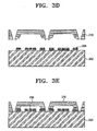
- FIG. 3D is a view for showing the etching of the photosensitive solution 302 coated in FIG. 3B and the seed layer 300 coated in FIG. 3A .
- the etching of the photosensitive solution 302 forms the first inductor 206 of the inductor device.
- FIG. 3D also shows the first protection package 210 to hermetically seal the first inductor 206.
- the first protection package 210 is made of glass, but can be made of a different substance depending on the user's requirement.
- FIG. 3E is a view for hermetically sealing the first inductor 206 with the first protection package 210.
- the first inductor 206 is hermetically sealed with the first protection package 210 by anodic bonding.
- a negative voltage is applied to the top of the first protection package 210 and a positive voltage is applied to the bottom of the substrate 202.
- a detailed description of the carrying-out of the anodic bonding will be omitted.
- the first inductor 206 is hermetically sealed with the first protection package 210 by the anodic bonding.
- the substrate 202 is polished to a certain thickness.
- the Chemical Mechanical Polishing (CMP) is used to polish the substrate 202.
- the flatness of the substrate 202 can be improved by the polishing of the substrate 202 by the CMP.
- FIG. 3G a portion of the substrate 202 is etched away to allow formation of a connection part 208 electrically connecting the first and second inductors 206 and 204. Further, FIG. 3G shows the etching of two regions to allow formation of two connection parts 208.
- FIG. 3H the regions etched away in FIG. 3G are electroplated with a metal substance to form the regions as the connection parts 208.
- the electroplating process is the same as shown in FIG. 3C .
- description will be made on a process of forming the second inductor 204.
- the second inductor 204 is formed.
- the process of forming the second inductor 204 is the same as the process carried out in FIGs. 3A to 3D .
- the photosensitive solution (PR) 306 is coated on a portion of the second inductor 204.
- FIG. 3J shows three regions, that is, both end portions and a middle portion, coated with the photosensitive solution 306, for example.
- a metal substance 304 is coated on the top of the first protection package 210.
- the metal substance can be replaced with the same substance as the metal substance 300 coated on the top of the substrate 202 of FIG. 3A .
- the process of coating the metal substance 304 can be omitted depending on user's requirement, or performed at one of the next steps to be carried out.
- a dry release is used to etch away the regions not coated with the photosensitive solution 306.
- the dry release etches away the substrate 202 not coated with the photosensitive solution 306.
- portions of the first and second inductors 206 and 204 can be etched away as the dry release is carried out.
- the dry-release process floats the first and second inductors 206 and 204 in the air.
- FIG. 3L the photosensitive solution 306 coated in FIG. 3J is removed.
- the second protection package 200 is used to hermetically seal the second inductor 204.
- the process of hermetically sealing the second inductor 204 is the same as the process of hermetically sealing the first inductor 206.
- electrodes are formed to supply electric currents to the first and second inductors 206 and 204.
- the electroplating is carried out to form the electrodes by filling a metal substance 212 in recess portions of the first protection package 210.
- the photosensitive solution 310 is coated on portions of the metal substance 212 to form the electrode layer 212 as in FIG. 2B .
- FIG. 3P shows a process of forming the first protection package for protecting the first inductor. Further, if the metal substance 212 is etched away, the photosensitive solution 310 coated in FIG. 3O is eliminated.
- FIGs. 3A-3P show a process of forming the first protection package for protecting the first inductor, but, depending on the user's requirement, the process can be omitted that forms the first protection package for protecting the first inductor as in FIG. 2A . That is, only the second protection package would be formed to protect the second inductor.
- the process for an inductor device according to the fabrication method of the present invention enables the inductor device to have high inductance and quality factor. Further, the method enables the inductor device to have air gaps of more than a few hundred ⁇ m formed therein.
- the method employs the dry-etching process instead of the much more difficult wet-etching process, enabling the flat and dual-structured inductors to be easily fabricated.
- the formation of the protection packages can protect the inductors from external shocks.
Landscapes
- Engineering & Computer Science (AREA)
- Power Engineering (AREA)
- Microelectronics & Electronic Packaging (AREA)
- Coils Or Transformers For Communication (AREA)
- Semiconductor Integrated Circuits (AREA)
- Manufacturing Cores, Coils, And Magnets (AREA)
Claims (9)
- Dispositif inductif, comprenant :un substrat gravé (202),des première (206) et deuxième (204) bobines d'inductance formées sur une partie supérieure et une partie inférieure du substrat (202), respectivement,des parties de connexion (208) destinées à connecter électriquement les première et deuxième bobines d'inductance, etun boîtier de protection (200, 210) destiné à protéger au moins une première des première et deuxième bobines d'inductance par rapport à l'extérieur,caractérisé parle fait que le substrat (202) fait l'objet d'un enlèvement de matière par gravure à des intervalles prédéterminés, en fournissant de cette manière un entrefer commun formé entre le substrat, la première bobine d'inductance (206) et la deuxième bobine d'inductance (204), afin que les première et deuxième bobines d'inductance soient exposées à l'air.
- Dispositif inductif selon la revendication 1, dans lequel les première et deuxième bobines d'inductance sont formées suivant une structure symétrique par rapport au substrat.
- Dispositif inductif selon la revendication 1, dans lequel un autre boîtier de protection protège l'autre des première et deuxième bobines d'inductance de l'extérieur.
- Dispositif inductif selon la revendication 1, dans lequel l'autre boîtier de protection a une couche d'électrode (304) formée sur celui-ci à des positions prédéterminées pour fournir des courants électriques au dispositif inductif.
- Procédé de production d'un dispositif inductif selon la revendication 1, comprenant les étapes consistant à :former une première bobine d'inductance (206) sur la partie supérieure d'un substrat (202), et former une deuxième bobine d'inductance (204) sur la partie inférieure du substrat,graver le substrat,connecter électriquement les première et deuxième bobines d'inductance, etformer un boîtier de protection (200, 210) pour sceller au moins une première de la première bobine d'inductance et de la deuxième bobine d'inductance pour protéger la au moins une première de la première bobine d'inductance et de la deuxième bobine d'inductance de l'extérieur,caractérisé en ce quele substrat fait l'objet d'un enlèvement de matière par gravure à des intervalles prédéterminés, en formant de cette manière un entrefer commun entre le substrat, la première bobine d'inductance et la deuxième bobine d'inductance, afin que les première et deuxième bobines d'inductance soient exposées à l'air.
- Procédé selon la revendication 5, dans lequel les première et deuxième bobines d'inductance sont formées suivant une structure symétrique par rapport au substrat.
- Procédé selon la revendication 5, dans lequel un autre boîtier de protection est formé pour sceller de manière hermétique l'autre des première et deuxième bobines d'inductance pour protéger l'autre des première et deuxième bobines d'inductance de l'extérieur.
- Procédé selon la revendication 5, dans lequel la couche d'électrode est formée à des positions prédéterminées sur l'autre boîtier de protection, de manière à fournir des courants électriques au dispositif inductif.
- Procédé selon la revendication 5, dans lequel le substrat est gravé par gravure sèche.
Applications Claiming Priority (1)
| Application Number | Priority Date | Filing Date | Title |
|---|---|---|---|
| KR1020040056468A KR100548388B1 (ko) | 2004-07-20 | 2004-07-20 | 저손실 인덕터소자 및 그의 제조방법 |
Publications (3)
| Publication Number | Publication Date |
|---|---|
| EP1619697A2 EP1619697A2 (fr) | 2006-01-25 |
| EP1619697A3 EP1619697A3 (fr) | 2006-03-22 |
| EP1619697B1 true EP1619697B1 (fr) | 2008-06-18 |
Family
ID=34937787
Family Applications (1)
| Application Number | Title | Priority Date | Filing Date |
|---|---|---|---|
| EP05014684A Expired - Lifetime EP1619697B1 (fr) | 2004-07-20 | 2005-07-06 | Dispositif inductif à faibles pertes et son procédé de fabrication |
Country Status (5)
| Country | Link |
|---|---|
| US (1) | US20060017539A1 (fr) |
| EP (1) | EP1619697B1 (fr) |
| JP (1) | JP4383392B2 (fr) |
| KR (1) | KR100548388B1 (fr) |
| DE (1) | DE602005007540D1 (fr) |
Families Citing this family (15)
| Publication number | Priority date | Publication date | Assignee | Title |
|---|---|---|---|---|
| US7255801B2 (en) * | 2004-04-08 | 2007-08-14 | Taiwan Semiconductor Manufacturing Company, Ltd. | Deep submicron CMOS compatible suspending inductor |
| KR100947933B1 (ko) * | 2007-08-28 | 2010-03-15 | 주식회사 동부하이텍 | 인덕터 및 그 제조 방법 |
| JP4815623B2 (ja) * | 2007-09-07 | 2011-11-16 | 三菱電機株式会社 | 高周波受動素子およびその製造方法 |
| CN101894861A (zh) * | 2009-05-22 | 2010-11-24 | 联发科技股份有限公司 | 半导体装置 |
| US8164159B1 (en) * | 2009-07-18 | 2012-04-24 | Intergrated Device Technologies, inc. | Semiconductor resonators with electromagnetic and environmental shielding and methods of forming same |
| DE102009045931B4 (de) * | 2009-10-22 | 2015-06-03 | Adidas Ag | Bekleidung |
| US9431473B2 (en) | 2012-11-21 | 2016-08-30 | Qualcomm Incorporated | Hybrid transformer structure on semiconductor devices |
| US10002700B2 (en) * | 2013-02-27 | 2018-06-19 | Qualcomm Incorporated | Vertical-coupling transformer with an air-gap structure |
| US9634645B2 (en) | 2013-03-14 | 2017-04-25 | Qualcomm Incorporated | Integration of a replica circuit and a transformer above a dielectric substrate |
| US9449753B2 (en) | 2013-08-30 | 2016-09-20 | Qualcomm Incorporated | Varying thickness inductor |
| US9906318B2 (en) | 2014-04-18 | 2018-02-27 | Qualcomm Incorporated | Frequency multiplexer |
| JP6405742B2 (ja) | 2014-06-26 | 2018-10-17 | 富士通株式会社 | コイル部品、及びコイル部品の製造方法 |
| JP6380028B2 (ja) * | 2014-11-13 | 2018-08-29 | 富士通株式会社 | インダクタの製造方法 |
| KR102113541B1 (ko) | 2018-08-07 | 2020-05-21 | 주식회사 이엠따블유 | 고주파 저손실 전극 |
| DE102020130092A1 (de) * | 2020-11-13 | 2022-05-19 | Wipotec Gmbh | Magnet-Spule-System |
Family Cites Families (21)
| Publication number | Priority date | Publication date | Assignee | Title |
|---|---|---|---|---|
| JPH0377360A (ja) * | 1989-08-18 | 1991-04-02 | Mitsubishi Electric Corp | 半導体装置 |
| JPH0513682A (ja) * | 1991-07-02 | 1993-01-22 | Mitsubishi Electric Corp | 半導体装置 |
| US6492705B1 (en) * | 1996-06-04 | 2002-12-10 | Intersil Corporation | Integrated circuit air bridge structures and methods of fabricating same |
| US5798557A (en) * | 1996-08-29 | 1998-08-25 | Harris Corporation | Lid wafer bond packaging and micromachining |
| US6159385A (en) * | 1998-05-08 | 2000-12-12 | Rockwell Technologies, Llc | Process for manufacture of micro electromechanical devices having high electrical isolation |
| US6201287B1 (en) * | 1998-10-26 | 2001-03-13 | Micron Technology, Inc. | Monolithic inductance-enhancing integrated circuits, complementary metal oxide semiconductor (CMOS) inductance-enhancing integrated circuits, inductor assemblies, and inductance-multiplying methods |
| JP2000186931A (ja) * | 1998-12-21 | 2000-07-04 | Murata Mfg Co Ltd | 小型電子部品及びその製造方法並びに該小型電子部品に用いるビアホールの成形方法 |
| US6240622B1 (en) * | 1999-07-09 | 2001-06-05 | Micron Technology, Inc. | Integrated circuit inductors |
| JP2001044034A (ja) * | 1999-07-27 | 2001-02-16 | Fuji Electric Co Ltd | 平面型磁気素子 |
| JP3446681B2 (ja) * | 1999-09-28 | 2003-09-16 | 株式会社村田製作所 | 積層インダクタアレイ |
| KR100368930B1 (ko) * | 2001-03-29 | 2003-01-24 | 한국과학기술원 | 반도체 기판 위에 높이 떠 있는 3차원 금속 소자, 그 회로모델, 및 그 제조방법 |
| KR100382765B1 (ko) * | 2001-06-15 | 2003-05-09 | 삼성전자주식회사 | 송수신용 수동소자와 그 집적모듈 및 그 제조방법 |
| US7671714B2 (en) * | 2001-08-09 | 2010-03-02 | Nxp B.V. | Planar inductive component and a planar transformer |
| US6856007B2 (en) * | 2001-08-28 | 2005-02-15 | Tessera, Inc. | High-frequency chip packages |
| US6518737B1 (en) * | 2001-09-28 | 2003-02-11 | Catalyst Semiconductor, Inc. | Low dropout voltage regulator with non-miller frequency compensation |
| JP3792635B2 (ja) * | 2001-12-14 | 2006-07-05 | 富士通株式会社 | 電子装置 |
| KR100465233B1 (ko) * | 2002-03-05 | 2005-01-13 | 삼성전자주식회사 | 저손실 인덕터소자 및 그의 제조방법 |
| JP4159378B2 (ja) * | 2002-04-25 | 2008-10-01 | 三菱電機株式会社 | 高周波装置とその製造方法 |
| US7147604B1 (en) * | 2002-08-07 | 2006-12-12 | Cardiomems, Inc. | High Q factor sensor |
| KR100477547B1 (ko) * | 2002-08-09 | 2005-03-18 | 동부아남반도체 주식회사 | 반도체 소자의 인덕터 형성방법 |
| US7255801B2 (en) * | 2004-04-08 | 2007-08-14 | Taiwan Semiconductor Manufacturing Company, Ltd. | Deep submicron CMOS compatible suspending inductor |
-
2004
- 2004-07-20 KR KR1020040056468A patent/KR100548388B1/ko not_active Expired - Fee Related
-
2005
- 2005-07-06 DE DE602005007540T patent/DE602005007540D1/de not_active Expired - Lifetime
- 2005-07-06 EP EP05014684A patent/EP1619697B1/fr not_active Expired - Lifetime
- 2005-07-20 US US11/184,999 patent/US20060017539A1/en not_active Abandoned
- 2005-07-20 JP JP2005210618A patent/JP4383392B2/ja not_active Expired - Fee Related
Also Published As
| Publication number | Publication date |
|---|---|
| KR100548388B1 (ko) | 2006-02-02 |
| EP1619697A2 (fr) | 2006-01-25 |
| KR20060007618A (ko) | 2006-01-26 |
| DE602005007540D1 (de) | 2008-07-31 |
| JP4383392B2 (ja) | 2009-12-16 |
| US20060017539A1 (en) | 2006-01-26 |
| JP2006032976A (ja) | 2006-02-02 |
| EP1619697A3 (fr) | 2006-03-22 |
Similar Documents
| Publication | Publication Date | Title |
|---|---|---|
| EP1619697B1 (fr) | Dispositif inductif à faibles pertes et son procédé de fabrication | |
| US7417525B2 (en) | High efficiency inductor, method for manufacturing the inductor, and packaging structure using the inductor | |
| CN102479605B (zh) | 变压器器件和用于制造变压器器件的方法 | |
| US6429764B1 (en) | Microcomponents of the microinductor or microtransformer type and process for fabricating such microcomponents | |
| US11094447B2 (en) | Chip inductor and method for manufacturing the same | |
| US10566126B2 (en) | Chip inductor and manufacturing method thereof | |
| TWI426572B (zh) | 微機電感測裝置及其製造方法 | |
| WO2001056920A2 (fr) | Dispositif a systeme micro-electromecanique | |
| KR20060136202A (ko) | 기판 매립형 인덕터 및 그 제조방법과, 마이크로 소자패키지 및 이 마이크로 소자 패키지의 캡 제조방법 | |
| EP2999002A1 (fr) | Cellule de condensateur et son procédé de fabrication | |
| CN110959188A (zh) | 电容器 | |
| JP4509152B2 (ja) | 薄膜圧電トランスおよびその製造方法 | |
| JP4916715B2 (ja) | 電子部品 | |
| JP6813058B2 (ja) | 振動子の製造方法 | |
| US7473981B2 (en) | Electronic component | |
| US8343791B2 (en) | Plating process and apparatus for through wafer features | |
| JP2022536515A (ja) | 複数ダイを備えるicパッケージ | |
| US20050093667A1 (en) | Three-dimensional inductive micro components | |
| CN102005439A (zh) | 高频器件 | |
| JP2004071481A (ja) | マイクロリレー及びその製造方法 | |
| EP4475172B1 (fr) | Structure d'isolation | |
| CN106531881B (zh) | 电磁阻抗感测元件及其制作方法 | |
| JP2010016240A (ja) | インダクタとその製造方法 | |
| CN112670272B (zh) | 半导体装置和制造半导体装置的方法 | |
| CN113474871B (zh) | 半导体装置 |
Legal Events
| Date | Code | Title | Description |
|---|---|---|---|
| PUAI | Public reference made under article 153(3) epc to a published international application that has entered the european phase |
Free format text: ORIGINAL CODE: 0009012 |
|
| 17P | Request for examination filed |
Effective date: 20050706 |
|
| AK | Designated contracting states |
Kind code of ref document: A2 Designated state(s): AT BE BG CH CY CZ DE DK EE ES FI FR GB GR HU IE IS IT LI LT LU LV MC NL PL PT RO SE SI SK TR |
|
| AX | Request for extension of the european patent |
Extension state: AL BA HR MK YU |
|
| PUAL | Search report despatched |
Free format text: ORIGINAL CODE: 0009013 |
|
| AK | Designated contracting states |
Kind code of ref document: A3 Designated state(s): AT BE BG CH CY CZ DE DK EE ES FI FR GB GR HU IE IS IT LI LT LU LV MC NL PL PT RO SE SI SK TR |
|
| AX | Request for extension of the european patent |
Extension state: AL BA HR MK YU |
|
| 17Q | First examination report despatched |
Effective date: 20060724 |
|
| AKX | Designation fees paid |
Designated state(s): DE FR GB |
|
| 17Q | First examination report despatched |
Effective date: 20060724 |
|
| GRAP | Despatch of communication of intention to grant a patent |
Free format text: ORIGINAL CODE: EPIDOSNIGR1 |
|
| GRAS | Grant fee paid |
Free format text: ORIGINAL CODE: EPIDOSNIGR3 |
|
| GRAA | (expected) grant |
Free format text: ORIGINAL CODE: 0009210 |
|
| AK | Designated contracting states |
Kind code of ref document: B1 Designated state(s): DE FR GB |
|
| REG | Reference to a national code |
Ref country code: GB Ref legal event code: FG4D |
|
| REF | Corresponds to: |
Ref document number: 602005007540 Country of ref document: DE Date of ref document: 20080731 Kind code of ref document: P |
|
| PLBE | No opposition filed within time limit |
Free format text: ORIGINAL CODE: 0009261 |
|
| STAA | Information on the status of an ep patent application or granted ep patent |
Free format text: STATUS: NO OPPOSITION FILED WITHIN TIME LIMIT |
|
| 26N | No opposition filed |
Effective date: 20090319 |
|
| PGFP | Annual fee paid to national office [announced via postgrant information from national office to epo] |
Ref country code: DE Payment date: 20130702 Year of fee payment: 9 |
|
| PGFP | Annual fee paid to national office [announced via postgrant information from national office to epo] |
Ref country code: FR Payment date: 20130726 Year of fee payment: 9 Ref country code: GB Payment date: 20130703 Year of fee payment: 9 |
|
| REG | Reference to a national code |
Ref country code: DE Ref legal event code: R119 Ref document number: 602005007540 Country of ref document: DE |
|
| GBPC | Gb: european patent ceased through non-payment of renewal fee |
Effective date: 20140706 |
|
| REG | Reference to a national code |
Ref country code: FR Ref legal event code: ST Effective date: 20150331 |
|
| PG25 | Lapsed in a contracting state [announced via postgrant information from national office to epo] |
Ref country code: DE Free format text: LAPSE BECAUSE OF NON-PAYMENT OF DUE FEES Effective date: 20150203 |
|
| REG | Reference to a national code |
Ref country code: DE Ref legal event code: R119 Ref document number: 602005007540 Country of ref document: DE Effective date: 20150203 |
|
| PG25 | Lapsed in a contracting state [announced via postgrant information from national office to epo] |
Ref country code: FR Free format text: LAPSE BECAUSE OF NON-PAYMENT OF DUE FEES Effective date: 20140731 Ref country code: GB Free format text: LAPSE BECAUSE OF NON-PAYMENT OF DUE FEES Effective date: 20140706 |
|
| P01 | Opt-out of the competence of the unified patent court (upc) registered |
Effective date: 20230520 |