EP1621971A2 - Circuit et procédé pour contrôler un circuit de protection contre les coupures de courant - Google Patents
Circuit et procédé pour contrôler un circuit de protection contre les coupures de courant Download PDFInfo
- Publication number
- EP1621971A2 EP1621971A2 EP05010988A EP05010988A EP1621971A2 EP 1621971 A2 EP1621971 A2 EP 1621971A2 EP 05010988 A EP05010988 A EP 05010988A EP 05010988 A EP05010988 A EP 05010988A EP 1621971 A2 EP1621971 A2 EP 1621971A2
- Authority
- EP
- European Patent Office
- Prior art keywords
- circuit
- graphics controller
- switch
- reset signal
- peripheral
- Prior art date
- Legal status (The legal status is an assumption and is not a legal conclusion. Google has not performed a legal analysis and makes no representation as to the accuracy of the status listed.)
- Withdrawn
Links
Images

Classifications
-
- G—PHYSICS
- G06—COMPUTING OR CALCULATING; COUNTING
- G06F—ELECTRIC DIGITAL DATA PROCESSING
- G06F1/00—Details not covered by groups G06F3/00 - G06F13/00 and G06F21/00
- G06F1/26—Power supply means, e.g. regulation thereof
- G06F1/30—Means for acting in the event of power-supply failure or interruption, e.g. power-supply fluctuations
Definitions
- This invention relates to a circuit and method for controlling a power cut-off protection circuit, particularly for use in a system including a graphics controller and a peripheral. More particularly, the invention relates to such a circuit and method for protecting the graphics controller from damage due to a loss of the power commonly supplied to the peripheral and the graphics controller.
- Graphics display systems typically employ a graphics controller chip between a host CPU and a graphics display device, such as an LCD panel.
- a graphics controller chip between a host CPU and a graphics display device, such as an LCD panel.
- graphics controller also include one or more peripheral devices.
- peripheral devices For example, in cellular telephones it is becoming increasingly common to couple a camera peripheral to the graphics controller. Both the camera and the host CPU are capable of providing corresponding sets of image data.
- the graphics controller can select between the sets of data for provision to the display device, or the graphics controller can overlay one set of data on the other set of data for provision to the display device.
- the graphics controller receives image data from the peripheral.
- the graphics controller could provide data to the peripheral.
- data exchanged between the graphics controller and the peripheral must typically be level shifted because the graphics controller and the peripheral are typically powered at different voltage levels.
- the graphics controller includes a level shifter for, e.g., each bit of a parallel data bus.
- the level shifters are typically formed of CMOS technology.
- the graphics controller includes a pin for receiving power from the peripheral to provide to one side of each level shifter with power while, internally, power used by the graphics controller is provided to the other side of the level shifters. So long as the power from the peripheral is "on,” the level shifters function normally.
- damage to the level shifters can result from CMOS latch-up if the peripheral is powered down while the graphics controller remains powered up. Yet it is often desired to power down the peripheral while the graphics controller remains powered up, for example, to reduce power consumption when processing an image received from the peripheral.
- the power cut-off protection circuit is controlled by another circuit that includes a register to which the host CPU writes at substantially the same time that the host CPU powers down the peripheral.
- the contents of the register are used to turn on respective MOSFETs connecting the level shifters to ground. This prevents CMOS latch-up in the level shifters when the power from the peripheral is cut-off.
- a preferred power cut-off protection control circuit and method according to the present invention is disclosed for use in a graphics controller.
- the graphics controller is controlled by a host and connected to a peripheral.
- the graphics controller includes a level shifter for shifting the voltage level of a signal received from the peripheral to a different voltage level suitable for processing the signal in the graphics controller.
- a switch is provided in a current path between the level shifter and ground. The switch is on or off in respective first and second control states of the switch.
- Preferred power cut-off control circuits include a memory pair and a selecting circuit.
- the memory pair stores data made available at respective storage inputs of first and second storage elements of the pair and provides the stored data at respective storage outputs thereof.
- the memory pair has a polarity selecting input through which the storage data output of one of the first and second storage elements is caused to correspond to the first control state of the switch and the storage data output of the other of the first and second storage elements is caused to correspond to the second control state of the switch.
- the selecting circuit has inputs coupled to the respective storage outputs of the memory pair and an output coupled to a control line of the switch for controlling the switch. A selecting line of the selecting circuit selects between the inputs, for selecting one or the other of the storage outputs of the first and second storage elements.
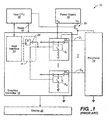
- Figure 1 shows a prior art circuit for controlling a power cut-off protection circuit 8 for a typical electronic computing and display system 10 having a graphics controller 12, a peripheral 14 such as a camera, a host CPU 16, a regulated power supply 18, and a graphics display device 20 such as an LCD panel.
- the graphics controller typically manages image data streaming from the camera and the CPU so as to combine the image data into a composite, and provides the composite data to the display device.
- the host CPU 16 communicates with the graphics controller 12 through a host interface 24 in the graphics controller.
- the host may be something other than a computer or CPU
- power cut-off control circuits and methods according to the invention may be practiced in chips or devices other than graphics controllers, so that no graphics display device is required
- the peripheral may be something other than a camera.
- the peripheral 14 typically provides a number of data lines D 1 - D N where N is typically 8.
- the power supply provides two voltage outputs V G and V P for powering the graphics controller 12 and the peripheral 14, respectively.
- the two voltages are each provided to respective sides of level shifters 22 1 and 22 N , where it is understood that there is a level shifter for each data line D.
- the level shifters provide level shifted data to the graphics controller for internal processing. However, the level shifters may be used to shift control signals or other signals as well.
- a register "R" is provided in the graphics controller for controlling switches S 1 - S N , which connect the respective level shifters 22 to ground when closed.
- the switches S function as power cut-off protection circuits.
- the switches are typically MOSFETS but may be of any desired technology.
- the host CPU 16 controls the power V P provided to the peripheral 14 as well as the graphics controller 12 by use of a switch 26, typically a MOSFET.
- the CPU turns off the switch 26 and then issues a command to the host interface 24 to write a "1" to the register "R.”
- the output of the register "R” is coupled to a buffer 28.
- the buffer 28 drives a signal for controlling the switches S.
- the buffer 28 drives a signal that turn the switches S on.
- the CPU 16 may instruct the graphics controller 12 to reset at any time by activating a reset line 30. If the graphics controller is reset, however, the content of the register "R" is lost, i.e., the "1" is replaced by a "0.” This turns the switches S off, resulting in large currents in the level shifters 22. This consumes power and can lead to CMOS latch-up.
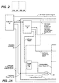
- FIG. 2 shows a preferred power cut-off protection control circuit 50 for an electronic computing and display system 30 according to the present invention.
- the system 30 includes a graphics controller 32.
- the system 30 also includes a peripheral 14, CPU 16, power supply 18, and graphics display device 20, and these components may be the same as those described above.
- the graphics controller 32 includes level shifters 22 1 and 22 N , each shifter having a switch "S", which functions as a power cut-off protection circuit.
- the preferred circuit 50 provides for either hardware or software control of cut-off protection circuits S 1 to S N .
- the peripheral 14 typically provides a number of data lines D 1 - D N for sending bits of data to the graphics controller in parallel. However, only one data line may be used for serial transmission of the data. Moreover, in an alternative embodiment, the peripheral 14 may receive bits of data on the data lines D 1 - D N .
- the power supply provides two voltage outputs V G and V P for powering the graphics controller 32 and the peripheral 14, respectively.
- the two voltages are each provided to respective sides of level shifters 22 1 and 22 N .
- the graphics controller includes a level shifter for each data line D.
- the level shifters provide level shifted data to the graphics controller for internal processing.
- the level shifters provide level shifted data to the peripheral.
- the switches S 1 - S N connect the respective level shifters 22 to ground, providing power cut-off protection.
- the switches are typically MOSFETS (NMOS or PMOS) but may be of any desired technology.
- the voltage output V P of the power supply 18 is connected or disconnected from the peripheral 14 and the level shifters 22 by control of a switch 34.
- a power control signal 36 is issued by the host 16 to turn the switch 34 on or off, thereby connecting or disconnecting the power V P to the peripheral 14 and the level shifters 22.
- the host CPU 16 communicates with the graphics controller 32 through a bus 45 connected to a host interface 44 in the graphics controller.
- the host interface 44 issues output bits as described below in response to instructions from the host.
- a preferred embodiment 50 of a circuit for controlling a power cut-off protection circuit according to the present invention is shown in Figure 2.
- the circuit 50 is provided on-board the graphics controller 32.
- the circuit 50 and variations of it may be implemented in hardware, firmware, software, or in any combination of these types of components, using any technology, in alternative embodiments as desired.
- a power cut-off multiplexer 52 directly drives the switches S of the power cut-off protection circuits.
- Each switch S has two control states. In the first control state, the switch S is on or closed. In the second control state, the switch S is off or open. Each switch S makes a current path between the respective level shifter and ground in the first control state, and breaks the path in the second control state.
- the switches are shown as being generic. Either a high or low signal from the multiplexer 52 may be employed to cause the switches S to enter a particular control state.
- the switches S are preferably MOSFETS, but may be a switch of any desired technology.
- the power cut-off multiplexer 52 has two inputs: input 54 for hardware control and input 56 for software control.
- the inputs of the multiplexer 52 are selected by the output of a hardware enable latch 58, which is set by a hardware control enable bit output on line 33 of the host interface 44.
- the hardware control enable bit selects between hardware control and software control of the power cut-off protection circuit. In the shown embodiment, setting the hardware control enable bit to "1" selects hardware control. In hardware control mode, the host CPU controls the power cut-off protection circuit via a pin 49 on the graphics controller 32.
- Hardware control is preferably implemented in the circuit 50 with a logic circuit that includes an exclusive OR gate 60 and a pin 49 polarity latch 62.
- This logic circuit uses the power control signal 36, which it obtains on a pin 49 of the graphics controller.
- the host uses the power control signal 36 to connect and disconnect the power V P to the peripheral 14. While the use of the one signal 36 to control both V P and the switches S is advantageous, it is not necessary for this logic circuit to use the power control signal 36.
- this circuit uses a signal on pin 49 that is dedicated for hardware control of the switches S.
- the pin 49 polarity latch 62 is set by a hardware configuration polarity bit which is provided on a line 37 of the host interface 44.
- the hardware polarity bit is configured by the host to assume the value ("1" or "0"), as required to ensure that the switches S are in the first control state (on or closed) when the output V P is disconnected.
- the power control signal 36 and the output of a latch 62 are input to the exclusive OR gate 60.
- the output 54 of the exclusive OR gate 60 is coupled to a first input of the power cut-off multiplexer 52.
- An example illustrates the hardware control mode. Assume that the peripheral power output V P is disconnected when the power control signal 36 is low. Also assume that the switches S are placed in their first control state (turned on) when an input 54 to the power cut-off multiplexer 52 is high. Setting the hardware polarity bit high (stored in the pin 49 polarity latch 62) causes the exclusive OR gate 60, when the power control signal 36 is low, to provide an output that is high. This high signal is passed through the multiplexer 52 to turn on the switches S when the peripheral power V P is disconnected.
- the host 16 turns the peripheral 14 back on by providing it with power V P .
- the host 16 provides power V P by turning the switch 34 back on.
- the host does this by causing the power control signal 36 to transition high.
- The causes the output 54 of the exclusive OR gate 60 to toggle.
- the output of the exclusive OR 60 will go low, turning the switches S off.
- the switches S are off.
- the hardware polarity bit held in the pin 49 polarity latch 62 will be reset if the graphics controller 32 is reset.
- a reset of the graphics controller is indicated by a reset signal provided on a line 42.
- the reset signal can be asserted as a result of a number of different influences and is referred to as a "cumulative" reset signal.
- the cumulative reset signal may result from instruction of the host 16, either through a hardware signal, bit or code provided at hardware reset pin 46 of the graphics controller 32, or as a software instruction issued through the host interface 44 to a reset latch 38.
- the graphics controller itself may generate an internal reset signal, bit or code.
- signals, bits, codes e.g., bytes
- these are generically referred to herein as "indications.”
- Another logic circuit selects any of the aforementioned routes for resetting the graphics controller.
- a three-input OR gate 40 generates the cumulative reset signal on line 42.
- a first input to OR gate 40 is coupled reset latch 38.
- a second input is coupled to the hardware reset pin 46.
- a third input is coupled an internal reset signal.
- the output of the OR gate 40 is coupled to line 42.
- Line 42 is coupled to the latches 58, 62, a and b.
- the content stored in the pin 49 polarity latch 62 is reset to "0" when the cumulative reset signal is asserted on line 42. Therefore, if the hardware polarity bit stored in latch 62 was a "1" to place the switches S in a first control state (on), then the switches S will turn off as the result of a cumulative reset signal being asserted on line 42 during a time when the power V P is disconnected from the peripheral. This result is undesirable.
- the circuit 50 connects the cumulative reset signal on line 42 to the hardware enable latch 58. Resetting the latch 58 controls the power cut-off multiplexer 52 to select software control. As described below, when operating under hardware control with V P off, this selection of software control prevents the undesirable change in state of the switches S.
- the host may, at any time, re-select hardware control by writing a "1" to the hardware enable latch 58.
- Software control is implemented in the preferred embodiment 50 by writing a "0" to the hardware enable latch 58. This zero may be written either, in the "normal” case, through the software interface, or by resetting the graphics controller 32.
- the output of the latch 58 selects the output 56 of a second multiplexer 64 as an input 56 to the power cut-off multiplexer 52 for driving the switches S.
- the second multiplexer 64 selects between a pair 66 of memory storage elements, particularly R-S latches "a” and “b" ("latch pair"), under control of a software configuration polarity signal that is made available at a pin 48 of the graphics controller 32.
- Each latch has a data storage input “D” (D a , D b ) and a corresponding data storage output "Q" (Q a , Q b ) for outputting latched data from the data storage input.
- One of the latches "a” has a reset input “R” and the other latch “b” has a set input "S”.
- the inputs R and S are tied together and form, in a preferred embodiment, a polarity selecting input 69 that is coupled to the reset and set inputs of the latches "a” and "b.”
- a software power-on bit is provided on a line 67 of the host interface 44 to both data storage inputs D of the latches "a” and “b.”
- the latches "a” and “b” therefore produce the same data storage outputs Q under normal operation. Where both latches of the latch pair produce the same data storage output, the software configuration polarity signal on pin 48 does not affect the output 56 of the second multiplexer 64.
- the software polarity bit provided on line 67 is set by the host as is appropriate for controlling the switches S as desired and provides the flexibility of interfacing to switches S that are placed in the first control state by either a high or low signal.
- the software power-on bit on line 67 should be low to maintain the switches off.
- the host toggles the software power-on bit on line 67 from low to high turning the switches S on.
- the host can regain control of the switches "S" by manipulating the software power-on bit on line 67. It should be readily apparent that the same degree of control can be provided under software control for any variation of the circuit shown in Figure 2, through use of the software power-on bit and the software configuration polarity signal, so long as the host 16 is made aware of the circuit requirements. As mentioned previously, the host may also re-select hardware control through use of the hardware enable latch 58.
- Power cut-off circuits and methods according to the present invention may be implemented in hardware or software, or both, and may employ machine readable media embodying one or more programs of instruction executed by the machine as will be readily apparent to persons of ordinary skill in the art.
Landscapes
- Engineering & Computer Science (AREA)
- Theoretical Computer Science (AREA)
- Physics & Mathematics (AREA)
- General Engineering & Computer Science (AREA)
- General Physics & Mathematics (AREA)
- Power Sources (AREA)
- Emergency Protection Circuit Devices (AREA)
Applications Claiming Priority (1)
| Application Number | Priority Date | Filing Date | Title |
|---|---|---|---|
| US10/902,542 US7191352B2 (en) | 2004-07-29 | 2004-07-29 | Circuit and method for controlling a power cut-off protection circuit |
Publications (2)
| Publication Number | Publication Date |
|---|---|
| EP1621971A2 true EP1621971A2 (fr) | 2006-02-01 |
| EP1621971A3 EP1621971A3 (fr) | 2009-10-28 |
Family
ID=35063417
Family Applications (1)
| Application Number | Title | Priority Date | Filing Date |
|---|---|---|---|
| EP05010988A Withdrawn EP1621971A3 (fr) | 2004-07-29 | 2005-05-20 | Circuit et procédé pour contrôler un circuit de protection contre les coupures de courant |
Country Status (4)
| Country | Link |
|---|---|
| US (1) | US7191352B2 (fr) |
| EP (1) | EP1621971A3 (fr) |
| JP (1) | JP4240019B2 (fr) |
| CN (1) | CN100365541C (fr) |
Families Citing this family (8)
| Publication number | Priority date | Publication date | Assignee | Title |
|---|---|---|---|---|
| DE10259708A1 (de) * | 2002-12-19 | 2004-07-08 | Basf Ag | Verbesserte Neutralisation von Isophoronnitril-Syntheseausträgen |
| US7876302B2 (en) * | 2004-07-26 | 2011-01-25 | Seiko Epson Corporation | Driving circuit for electro-optical panel and driving method thereof, electro-optical device, and electronic apparatus having electro-optical device |
| KR100698140B1 (ko) * | 2004-10-05 | 2007-03-26 | 엘지전자 주식회사 | 방송 수신이 가능한 이동 단말기의 전원 패스 장치 |
| JP5076317B2 (ja) * | 2005-12-27 | 2012-11-21 | ソニー株式会社 | 情報処理装置、情報処理方法及びそのプログラム |
| US7944769B1 (en) * | 2009-10-14 | 2011-05-17 | Xilinx, Inc. | System for power-on detection |
| JP5601599B2 (ja) * | 2013-03-13 | 2014-10-08 | Necプラットフォームズ株式会社 | デバイス接続システム、携帯端末、デバイス接続方法及びデバイス接続プログラム |
| US10915484B2 (en) * | 2017-02-24 | 2021-02-09 | Digital 14 Llc | Peripheral disconnection switch system and method |
| CN111474924B (zh) * | 2019-01-23 | 2023-12-26 | 菜鸟智能物流控股有限公司 | 控制设备、控制装置、控制方法和物流对象处理系统 |
Family Cites Families (17)
| Publication number | Priority date | Publication date | Assignee | Title |
|---|---|---|---|---|
| US4454575A (en) * | 1980-12-29 | 1984-06-12 | International Business Machines Corporation | Shared memory system with access by specialized peripherals managed by controller initialized by supervisory CPU |
| CA2027799A1 (fr) * | 1989-11-03 | 1991-05-04 | David A. Miller | Methode et dispositif pour reinitialiser individuellement les processeurs et les controleurs d'antememoire dans les systeme multiprocesseurs |
| US6101600A (en) * | 1996-03-01 | 2000-08-08 | Compaq Computer Corporation | Resetting a CPU |
| JP3266560B2 (ja) * | 1998-01-07 | 2002-03-18 | インターナショナル・ビジネス・マシーンズ・コーポレーション | 情報処理システム及びその制御方法 |
| US6429716B1 (en) * | 1998-12-14 | 2002-08-06 | Ati International Srl | Pre-buffer voltage level shifting circuit and method |
| JP3473745B2 (ja) * | 1999-05-28 | 2003-12-08 | シャープ株式会社 | シフトレジスタ、および、それを用いた画像表示装置 |
| JP2000353946A (ja) * | 1999-06-10 | 2000-12-19 | Matsushita Electric Ind Co Ltd | レベルシフタ回路 |
| US6526514B1 (en) * | 1999-10-11 | 2003-02-25 | Ati International Srl | Method and apparatus for power management interrupt processing in a computing system |
| US6654896B1 (en) * | 2000-05-16 | 2003-11-25 | Hewlett-Packard Development Company, L.P. | Handling of multiple compliant and non-compliant wake-up sources in a computer system |
| US7017056B1 (en) * | 2000-07-31 | 2006-03-21 | Hewlett-Packard Development Company, L.P. | Method and apparatus for secure remote control of power-on state for computers |
| US6608476B1 (en) * | 2000-09-26 | 2003-08-19 | Sun Microsystems, Inc. | Method and apparatus for reducing power consumption |
| US7184014B2 (en) * | 2000-10-05 | 2007-02-27 | Semiconductor Energy Laboratory Co., Ltd. | Liquid crystal display device |
| US6700407B1 (en) * | 2001-12-04 | 2004-03-02 | National Semiconductor Corporation | Extended voltage range level shifter |
| JP2003196117A (ja) * | 2001-12-26 | 2003-07-11 | Toshiba Corp | マイクロプロセッサ |
| JP3657235B2 (ja) * | 2002-03-25 | 2005-06-08 | Necマイクロシステム株式会社 | レベルシフタ回路及び該レベルシフタ回路を備えた半導体装置 |
| US7027056B2 (en) * | 2002-05-10 | 2006-04-11 | Nec Electronics (Europe) Gmbh | Graphics engine, and display driver IC and display module incorporating the graphics engine |
| US6894537B1 (en) * | 2002-12-18 | 2005-05-17 | National Semiconductor Corporation | Apparatus and method for level shifting in power-on reset circuitry in dual power supply domains |
-
2004
- 2004-07-29 US US10/902,542 patent/US7191352B2/en not_active Expired - Fee Related
-
2005
- 2005-05-20 EP EP05010988A patent/EP1621971A3/fr not_active Withdrawn
- 2005-07-29 CN CNB2005100882385A patent/CN100365541C/zh not_active Expired - Fee Related
- 2005-07-29 JP JP2005220467A patent/JP4240019B2/ja not_active Expired - Fee Related
Also Published As
| Publication number | Publication date |
|---|---|
| CN1734398A (zh) | 2006-02-15 |
| JP4240019B2 (ja) | 2009-03-18 |
| EP1621971A3 (fr) | 2009-10-28 |
| JP2006040294A (ja) | 2006-02-09 |
| US20060022988A1 (en) | 2006-02-02 |
| US7191352B2 (en) | 2007-03-13 |
| CN100365541C (zh) | 2008-01-30 |
Similar Documents
| Publication | Publication Date | Title |
|---|---|---|
| US7167991B2 (en) | Method for reducing leakage current of LSI | |
| US20120326764A1 (en) | Mipi analog switch for automatic selection of multiple image sensors | |
| US7263622B2 (en) | Power-saving device for controlling circuit operation, and information processing apparatus | |
| US8330518B2 (en) | Low consumption flip-flop circuit with data retention and method thereof | |
| US8913048B2 (en) | Source driver circuit of liquid crystal display device | |
| EP1621971A2 (fr) | Circuit et procédé pour contrôler un circuit de protection contre les coupures de courant | |
| JPS59200326A (ja) | データ処理装置 | |
| JPH09219637A (ja) | 駆動回路 | |
| US11322187B2 (en) | Protection circuit for memory in display panel and display panel | |
| US20060076987A1 (en) | Multi-threshold CMOS system having short-circuit current prevention circuit | |
| KR101062845B1 (ko) | 글로벌 라인 제어회로 | |
| US20060079120A1 (en) | Interface and control devices for display apparatus and integrated circuit chip having the same | |
| JP2005234976A (ja) | 記憶装置 | |
| US7403036B2 (en) | Interface circuit | |
| US6593775B2 (en) | Insulatior for a multi-power system | |
| JP2006048304A (ja) | マイクロコンピュータ | |
| JP2009141396A (ja) | ハザード対策回路、出力回路および半導体装置 | |
| JP3615189B2 (ja) | 入出力バッファ回路 | |
| CN100371980C (zh) | 显示控制装置 | |
| US7058842B2 (en) | Microcontroller with multiple function blocks and clock signal control | |
| US20040169199A1 (en) | Semiconductor integrated circuit and interrupt request output method thereof | |
| US20090243693A1 (en) | Circuit for providing deterministic logic level in output circuit when a power supply is grounded | |
| US20250231900A1 (en) | Usb routing integrated circuit with multiple usb upstream ports and operation method thereof | |
| US7398404B2 (en) | System and related control device and method for controlling power supply according to a power status | |
| JP2005284672A (ja) | 通信装置 |
Legal Events
| Date | Code | Title | Description |
|---|---|---|---|
| PUAI | Public reference made under article 153(3) epc to a published international application that has entered the european phase |
Free format text: ORIGINAL CODE: 0009012 |
|
| AK | Designated contracting states |
Kind code of ref document: A2 Designated state(s): AT BE BG CH CY CZ DE DK EE ES FI FR GB GR HU IE IS IT LI LT LU MC NL PL PT RO SE SI SK TR |
|
| AX | Request for extension of the european patent |
Extension state: AL BA HR LV MK YU |
|
| PUAL | Search report despatched |
Free format text: ORIGINAL CODE: 0009013 |
|
| AK | Designated contracting states |
Kind code of ref document: A3 Designated state(s): AT BE BG CH CY CZ DE DK EE ES FI FR GB GR HU IE IS IT LI LT LU MC NL PL PT RO SE SI SK TR |
|
| AX | Request for extension of the european patent |
Extension state: AL BA HR LV MK YU |
|
| AKX | Designation fees paid | ||
| STAA | Information on the status of an ep patent application or granted ep patent |
Free format text: STATUS: THE APPLICATION IS DEEMED TO BE WITHDRAWN |
|
| 18D | Application deemed to be withdrawn |
Effective date: 20100429 |
|
| REG | Reference to a national code |
Ref country code: DE Ref legal event code: 8566 |