EP1622036A2 - Speicherungsgerätsystem und Signalübertragungsverfahren für Speicherungsgerätsystem - Google Patents
Speicherungsgerätsystem und Signalübertragungsverfahren für Speicherungsgerätsystem Download PDFInfo
- Publication number
- EP1622036A2 EP1622036A2 EP05252501A EP05252501A EP1622036A2 EP 1622036 A2 EP1622036 A2 EP 1622036A2 EP 05252501 A EP05252501 A EP 05252501A EP 05252501 A EP05252501 A EP 05252501A EP 1622036 A2 EP1622036 A2 EP 1622036A2
- Authority
- EP
- European Patent Office
- Prior art keywords
- signal
- storage device
- storage
- attribute
- boost
- Prior art date
- Legal status (The legal status is an assumption and is not a legal conclusion. Google has not performed a legal analysis and makes no representation as to the accuracy of the status listed.)
- Granted
Links
Images


Classifications
-
- G—PHYSICS
- G06—COMPUTING OR CALCULATING; COUNTING
- G06F—ELECTRIC DIGITAL DATA PROCESSING
- G06F13/00—Interconnection of, or transfer of information or other signals between, memories, input/output devices or central processing units
- G06F13/38—Information transfer, e.g. on bus
- G06F13/40—Bus structure
- G06F13/4063—Device-to-bus coupling
- G06F13/4068—Electrical coupling
- G06F13/4072—Drivers or receivers
-
- H—ELECTRICITY
- H04—ELECTRIC COMMUNICATION TECHNIQUE
- H04L—TRANSMISSION OF DIGITAL INFORMATION, e.g. TELEGRAPHIC COMMUNICATION
- H04L25/00—Baseband systems
- H04L25/02—Details ; arrangements for supplying electrical power along data transmission lines
- H04L25/03—Shaping networks in transmitter or receiver, e.g. adaptive shaping networks
- H04L25/03006—Arrangements for removing intersymbol interference
- H04L25/03343—Arrangements at the transmitter end
Definitions
- the present invention relates to a storage device system, and more particularly, to a technology for transmitting signals to a plurality of storage devices installed in a storage device system.
- a disk array device provided with a fiber channel loop, a control device and a plurality of disk devices is known.
- the control device and the plurality of disk devices are connected to the fiber channel loop.
- the control device accesses any one of the plurality of disk devices, via the fiber channel loop.
- FC-AL Fiber Channel Arbitrated Loop
- HDDs for serial interfaces are also known, such as an HDD for a SATA (Serial AT Attachment) system, and an HDD for a SAS (Serial Attached SCSI) system.
- SATA Serial AT Attachment
- SAS Serial Attached SCSI
- One example of an HDD for a SATA system is known which is capable of transferring data at a speed of 1.5 Gbps, but it is hoped that HDDs for both SATA and SAS systems capable of even faster data transfer, such as data transfer speeds of 3 Gbps or above, will also be developed.
- signal loss can be envisaged due to one or more than one problem, such as signal loss caused by the skin effect of the printed circuit boards or by dielectric loss, or signal loss caused by impedance mismatching of the interface connectors which connect the printed circuit boards with the HDD S .
- signal loss caused by the skin effect of the printed circuit boards or by dielectric loss, or signal loss caused by impedance mismatching of the interface connectors which connect the printed circuit boards with the HDD S .
- a high frequency signal exceeding 1 GHz is required.
- the transmission frequency is less than 1 GHz, then signal attenuation will occur principally due to conductor loss, but if the frequency exceeds 1 GHz, then signal attenuation will occur principally due to dielectric loss. It is thought that the increase in dielectric loss in the printed circuit board becomes particularly problematic, if the transmission frequency exceeds 1 GHz in the signal path through the printed circuit board (for example, if the transmission frequency is 2 GHz or above). This is because if the dielectric loss increases, then the leakage current also increases, thus degrading the signal quality. Consequently, degradation of signal quality is expected to be a problem if an HDD capable of high-speed serial data transfer is installed in a disk array device.
- the length of the transmission path in the printed circuit board connecting the control device with the HDDs may be equal to or exceed a certain value (for example, 100 mm). Therefore, deterioration of the signal quality due to transmission loss is also thought to be a potential problem.
- HDDs of different HDD types for example, FC, SATA or SAS
- HDDs having different data transfer speeds for example, FC, SATA or SAS
- ISI Inter Symbol Interference
- HDDs from different providers (such as different manufacturers or vendors) (for example, HDDs from a different provider to the provider of the disk array device), in the disk array device.
- HDDs from different providers (such as different manufacturers or vendors)
- HDDs from a different provider to the provider of the disk array device
- reflections may be produced by slight impedance mismatches in the impedance profile between the signal transmission paths in the printed circuit boards and the HDDs, and signal quality may also be degraded by these reflections. This becomes particularly notable, the higher the data transfer speed.
- the problems described above are not limited to disk array devices provided with HDDs, and they may also appear in storage device systems provided with a plurality of storage devices of another type (such as DVD (Digital Versatile Disk) drives).
- DVD Digital Versatile Disk
- one object of the present invention is to prevent degradation of signal quality during transmission from or to a plurality of storage devices. More specifically, for example, one object of the present invention is to prevent degradation of signal quality during transmission from or to a plurality of storage devices using high-speed serial transfer, where dielectric loss is the dominant factor in signal degradation. It is also an object of the present invention to prevent degradation of signal quality during transmission to or from storage devices, even if the plurality of storage devices include storage devices having a transmission path which exceeds a prescribed length. It is also an object of the present invention to prevent degradation of signal quality during transmission to or from a plurality of storage devices having different storage device attributes (for example, at least one attribute out of the data transfer speed, the device type and the device provider).
- storage device attributes for example, at least one attribute out of the data transfer speed, the device type and the device provider.
- the storage device system comprises: a plurality of signal transmission paths connected respectively to a plurality of installed storage devices; a plurality of system side communications sections for transmitting and receiving signals respectively to and from the plurality of storage devices, via the plurality of signal transmission paths; and one or a plurality of signal correcting sections for inputting a signal exchanged between the plurality of storage devices and the plurality of system side communications sections, correcting the input signal on the basis of a previously established correction parameter, and outputting the corrected signal.
- the correction parameter is a value set on the basis of at least one of the length of the signal transmission path between the storage device and the system side communications section, the wavelength attribute (for example, the signal waveform pattern) of the signal input to the signal correcting section, and the storage device attribute relating to the storage device.
- the correction parameter is a signal boost value.
- each of the plurality of signal correcting sections boosts at least one of a signal transmitted by the storage device, a signal transmitted by the system side communications section, and a signal passing through the signal transmission path, on the basis of the boost value, and then transmits the boosted signal.
- the storage devices each comprise a storage device transmitting section for transmitting signals and a storage device receiving section for receiving signals.
- the system side communications sections comprise system signal transmitting sections for transmitting signals and system side receiving sections for receiving signals.
- the signal transmission paths comprise a first sub transmission path forming a signal transmission path between the storage device transmitting section and the system side receiving section, and a second sub signal transmission path forming a signal transmission path between the storage device receiving section and the system side transmitting section.
- the plurality of signal correcting sections are provided respectively in at least one of: the storage device transmitting section, the system side transmitting section, the first sub transmission path and the second sub transmission path, and they boost the input signal on the basis of the boost value and output the boosted value.
- the boost value is a value based on attenuation due to inter symbol interference corresponding to the length of the signal transmission path.
- the signal correcting section boosts the amplitude of the shortest wavelength signal, on the basis of the boost value, in such a manner that it has the same amplitude upon reception as the amplitude of the longest wavelength signal upon reception, and it outputs the boosted signal.
- the storage device attribute is at least one of the data transfer speed, the type or the provider of the storage device.
- the data transfer speed is a speed based on the signal frequency, where dielectric loss is more dominant than conductor loss (for example, a speed at which it is desirable to transmit signals at a high frequency of this kind).
- the first storage device system further comprises: a storage device attribute determining section for determining the storage device attribute of the installed storage device, on the basis of the installation configuration of the storage device; a correction parameter storage region for storing a plurality of correction parameters corresponding respectively to a plurality of types of the storage device attributes, and a correction parameter setting section for setting a correction parameter corresponding to the determined storage device attribute, and stored in the correction parameter storage region, in the signal correcting section of the plurality of signal correcting sections that relates to the installed storage device.
- a storage device attribute determining section for determining the storage device attribute of the installed storage device, on the basis of the installation configuration of the storage device
- a correction parameter storage region for storing a plurality of correction parameters corresponding respectively to a plurality of types of the storage device attributes
- a correction parameter setting section for setting a correction parameter corresponding to the determined storage device attribute, and stored in the correction parameter storage region, in the signal correcting section of the plurality of signal correcting sections that relates to the installed storage device.
- each of the plurality of storage devices is accommodated in a storage device casing, and is installed in the storage device system together with the storage device casing.
- the storage device casing comprises a casing connection section having a composition corresponding to the storage device attribute of the storage device accommodated in that storage device casing.
- the first storage device system comprises a system side connection section for connecting with the casing connection section.
- a storage device attribute identification signal having a waveform corresponding to the composition of the casing connection section is output when the casing connection section is connected to the system side connection section.
- the storage device attribute determining section determines the storage device attribute of the installed storage device, on the basis of the storage device attribute identification signal thus output.
- the signal transmission method is a signal transmission method for a storage device system in which a plurality of storage devices can be installed.
- the storage device system comprises: a plurality of signal transmission paths connected respectively to the plurality of installed storage devices, and a plurality of system side communications sections for transmitting and receiving signals respectively to and from the plurality of storage devices, via the plurality of signal transmission paths.
- the following steps (A) to (C) are implemented for each of the signal transmission paths; (A) a step of inputting a signal exchanged between a storage device and a system side communications section; (B) a step of correcting the input signal on the basis of a previously set correction parameter; and (C) a step of outputting the corrected signal.
- the correction parameter is a value established on the basis of any one of the length of the signal transmission path, the wavelength attribute of the input signal, and the storage device attribute relating to the storage device.
- the storage device system is a storage device control board, being a printed circuit board to which a storage device installation board is connected, for controlling the plurality of storage devices via the storage device installation board; a plurality of transmission circuits, provided on the storage device control board, for transmitting signals to the plurality of storage devices, respectively, via a plurality of first signal transmission paths; a plurality of reception circuits, provided on the storage device control board, for receiving signals from the plurality of storage devices, respectively, via a plurality of second signal transmission paths; a plurality of signal correcting devices provided respectively in the plurality of transmission circuits; a boost value storage region for storing a plurality of signal boost values determined on the basis of the signal attenuation corresponding to at least one of the length of the first signal transmission path, the signal wavelength attribute, and a storage device attribute relating to the storage device; a boost value setting region in which at least one of the plurality of signal boost values stored in the boost value storage region is set; and a processor for setting at
- the boost value setting region has a plurality of setting region addresses corresponding respectively to the plurality of transmission circuits.
- the processor sets, in each of the plurality of setting region addresses, the signal boost value to be used by the signal correction device provided in the transmission circuit corresponding to that setting region address, the signal boost value being determined on the basis of at least one of the length of the first signal transmission path for the signal transmitted by the corresponding transmission circuit, the wavelength attribute and the transmission destination of the signal from that transmission circuit.
- the signal correcting devices respectively input a signal, boost the input signal on the basis of the signal boost value set in the setting region address corresponding to the transmission circuit in which the signal correcting devices are provided, and output the boosted signal.
- Each of the plurality of storage devices may be accommodated in a storage device casing, and may be installed in the storage device system together with the storage device casing.
- the storage device casing may comprise a casing connection section having a composition corresponding to the storage device attribute of the storage device accommodated in that storage device casing.
- the storage device installation board may comprise a plurality of system side connection sections for connecting with the casing connection section.
- a storage device attribute identification signal having a waveform corresponding to the composition of the casing connection section may be output when the casing connection section is connected to the system side connection section.
- the processor may determine the storage device attribute of a storage device that has been installed, and the position on the storage device installation board at which the storage device has been installed, on the basis of the output source and the waveform of the storage device attribute identification signal, and set a signal boost value corresponding to the storage device attribute thus determined in the setting region address corresponding to the transmission circuit which transmits signals to the storage device installed at the installation position thus determined.
- Fig. 29A shows a schematic view of one mode of implementing the present invention.
- a signal correction section 1003 is provided for outputting a signal obtained by correcting an input signal (voltage signal) 1005 as an output signal 1007.
- the signal correction section 1003 corrects the input signal 1005 by using a correction parameter set in a prescribed storage region (not labeled with a reference numeral) .
- the correction parameter set in the prescribed storage region is a correction parameter selected from a correction parameter group 1001 on the basis of a signal attenuation cause.
- the correction parameter group 1001 comprises two or more correction parameter groups based on signal attenuation causes.
- the correction parameter group 1001 comprises two or more sub-groups corresponding to at least one of: a plurality of signal transmission distances (in other words, storage device installation positions), a plurality of transmission signal attributes, and a plurality of storage device attributes.
- One or more correction parameters are contained in each sub-group.
- the correction parameter set in the prescribed storage region is a correction parameter corresponding to an attenuation cause relating to input signal or a signal that is to be output (for example, corresponding to at least one of the signal transmission distance, the transmission signal attribute or the storage device attribute), and it is selected from the correction parameter group 1001.
- the correction parameter may be selected by the user, or it may be selected on the basis of an identified signal attenuation cause, by means of the hardware, the computer program or a combination of same, identifying the signal attenuation cause.
- Fig. 29B shows an example of the composition of an storage device system to which the concept of one mode of implementing the present invention is applied.
- the storage device system 1023 comprises a plurality of storage devices 1012 (for example, two storage devices), a storage device communications section 1031, and a storage control section 1021.
- Each of the storage devices 1012 comprises a storage resource (for example, a hard disk or DVD) 1013, and an interface section (not labeled with a reference numeral) corresponding to the storage resource 1013.
- the interface section comprises a receiving section 1015S for receiving a signal written to the storage resource 1013, and a transmitting section 1019S for transmitting a signal read out from the storage resource 1013.
- the storage device communications section 1031 is connected to the plurality of storage devices 1012, either directly or indirectly (for example, via a printed circuit board).
- the storage device communications section 1031 is a printed circuit board, for example, and comprises (one or) a plurality of transmitting sections 1019C, (one or) a plurality of receiving sections 1015C, and a switching device 1033.
- a first signal transmission path 1009 is provided between the transmitting section 1019C and the receiving section 1015S of a storage device 1012
- a second signal transmission path 1011 is provided between the receiving section 1015C and the transmitting section 1019S of a storage device 1012. Copper wires may be used for the first signal transmission path 1009 and/or the second signal transmission path 1011.
- the switch device 1033 is a switch for controlling the connection between the storage control section 1021 and the plurality of storage devices 1012, and is constituted by a fiber channel loop, for example.
- the storage control section 1035 accesses any one of the plurality of storage devices 1012 via the switch device 1033, in accordance with a request from an upper-level device 1035, and it reads out data from the storage device or writes data to the storage device.
- the signal correcting section 1003 described above may be located in various positions.
- signal correcting sections 1003 may be installed in the transmitting sections 1019S, 1019C, in the receiving sections 1015S, 1015C, in the signal transmission paths 1009 and/or 1011, in the transmitting sections 1019S and receiving sections 1015S (in other words, in the storage devices 1012), and/or in the transmitting sections 1019C and receiving sections 1015C (in other words, in the storage device communications section 1031).
- signal correcting sections 1003 may be installed in a variety of positions in this way, they may be of the same composition wherever they are positioned, or they may be of different compositions, depending on their location and the correction parameter. Furthermore, the correction parameter established with respect to each signal correcting section 1003 differs according to the attenuation cause relating to the signal input to or output from that signal correcting section 1003.
- a plurality of either transmitting sections 1019S and/or receiving sections 1015S may be provided in each storage device 1012. Moreover, a plurality of receiving sections 1015S may be connected to each transmitting section 1019C, and a plurality of transmitting sections 1019S may be connected to each receiving section 1015C. Similarly, a plurality of receiving sections 1015C may be connected to each transmitting section 1019S, and a plurality of transmitting sections 1019C may be connected to each receiving section 1015S.
- Fig. 1 shows an external view of the general composition of a disk array device relating to a first embodiment of one mode of implementing the present invention.
- the disk array device 1 comprises a controller frame 2a capable of accommodating a disk control device 2 and a canister 4 in a central position, and disk drive frames 3a capable of accommodating canisters 4, to the left and right-hand sides of the controller frame 2a.
- the canisters 4 contain disk drives.
- the disk drives it is possible to use various types of device, such as a hard disk drive (HDD), or a semiconductor storage device, or the like.
- the controller frame 2a corresponds to the basic frame and the disk drive frames 3a are so-called expansion frames, which may not be provided at all, or which may be provided in plural fashion.
- the control frame 2a controls the disk array device 1.
- the control frame 2a comprises, for example, a management terminal 5, a disk control device 2, cooling fans 7, a power supply unit 8, a battery, an AC box 10, an HDD control board 20, and the like.
- the management terminal 5 can be located in various positions, such as the front face of the controller frame 2a, for example.
- the management terminal 5 is, for example, a notebook computer, comprising a display device and a keyboard device which can be folded together and closed. By using this management terminal 5, an operator is able to maintain and manage the disk array device 1.
- the disk control device 2 is a machine for controlling the whole disk array device 1, and it comprises a plurality of control boards 6.
- the control boards 6 are, for example, circuits formed by providing circuit elements on a printed circuit board, and they constitute, for example, channel adapters (channel control sections), disk adapters (disk control sections), cache memories, shared memories, or the like, as described hereinafter.
- the cooling fans 7 are used to cool the disk control device 2 and the disk drives.
- the power supply unit 8 supplies a prescribed electric power to at least one of the plurality of constituent elements which make up the disk array device 1. In this way, the disk array device 1 can be driven.
- the PBC (Port Bypass Circuit) board 20 is described hereinafter.
- a plurality of canisters 4 (in other words, a plurality of disk drives) are provided in each disk drive frame 3a.
- Fig. 2A, Fig. 2B and Fig. 2C show the appearance of a disk drive frame 3a.
- Fig. 2A is a general front side view of a disk drive frame 3a.
- Fig. 2B is a general cross-sectional view of a disk drive frame 3a.
- Fig. 2C is a general rear side view of a disk drive frame 3c.
- each disk drive device 3 comprises, for example, a plurality of canister groups 41, 42, 43 and 44, and a plurality of HDD control boards 20a, 20b, 20c and 20d corresponding respectively to this plurality of canister groups 41, 42, 43 and 44.
- the plurality of HDD control boards 20a, 20b, 20c and 20d are connected to one (or a plurality of) back plane boards (for example, printed circuit boards) 22.
- the back plane boards 22 are connected to the disk drives 4a in a plurality of canisters 4 contained in the respective canister groups 41, 42, 43 or 44.
- the canisters 4 are not only stored on the front side of the disk array device 1 (in other words, the same side as the management terminal 5), but also on the rear side, as illustrated in Fig. 2C.
- the management terminal 5 does not need to be incorporated into the disk array device 1, and it may also be a computer that is connected to the disk array device 1 by means of a communications network.
- the management terminal 5 is not limited to being a notebook type computer, and it may also be a desktop computer, for example.
- the disk control device 2 and the disk drive devices 3 may be formed in an integrated fashion.
- an LED (light-emitting diode) display section may be provided on the front face or rear face of the disk array device 1, and the operational status of the respective disk drives 4a may be displayed by means of LEDs switching on or off, for example.
- Fig. 3A shows the connection layout between the disk control device 2 and the disk drive devices 3 in the disk array device 1.
- Fig. 3B shows the communication paths between the HDD control boards 20a and 20c in Fig. 3A and the plurality of canisters 4.
- the term “fiber channel” is abbreviated to "FC”.
- the term “HDD control board 20" is taken to indicate at least one of the plurality of HDD control boards 20a, 20b, 20c and 20d, or an HDD control board other than these.
- a plurality of disk adapters (hereinafter, abbreviated to "DKA”) 10 are provided in the disk control device 2, for example.
- Each pair DKA 10 and DKA 10 of the plurality of DKAs 10 constitutes a cluster, for example (in other words, there is a dual access system to each of the disk drives 4a) , and if a fault occurs in one DKA 10 and that DKA 10 becomes unable to access a certain disk drive 4a, then the other DKA 10 can access that disk drive 4a.
- FC cables metal cables, such as copper cables, for example
- the foremost HDD control board 20 of the two or more HDD control boards 20 connected in series is connected to the DKA 10, via an FC cable 13a.
- FC-AL Fiber Channel Arbitrated Loop
- FC-AL Fiber Channel Arbitrated Loop
- a plurality of FC loops are provided in the disk array device 1, and a plurality of disk drives 4a are connected to each FC loop, by means of the back plane board 22 (see Fig. 2B) , which is not illustrated in Fig. 3A and Fig. 3B.
- Each DKA 10 is able to access any of the plurality of disk drives 4a connected to the FC loop to which it is connected, via that FC loop.
- the disk drives 4a are HDDs (hard disk drives). As shown in Fig. 3B, FC HDDs may be used as the HDDs 4a, or SATA HDDs or SES HDDs may be used.
- FC HDD is an HDD composed in such a manner that it can be connected to an FC-AL, in accordance with fiber channel (FC) standards, and it has a data transfer speed of 1 Gbps - 2 Gbps, for example.
- the plurality of canisters 4 include canisters 4F of a type installed with an FC HDD of this kind.
- a DC/DC converter 4b is also installed in this canister 4F, in addition to the FC HDD. The DC/DC converter 4b lowers the DC voltage supplied from an external source and applies it to the FC HDD.
- a SATA (Serial AT Attachment) HDD is an HDD 4 which uses a serial transfer method instead of the parallel transfer method employed in ATA specifications, and it has a data transfer speed of 1.5 Gbps, for example.
- the SES (SCSI Enclosure Service) HDD is a disk drive capable of communicating with the DKAs 10 and power controller (not illustrated) controlling the power supply to the HDD 4a. It has SES or ESI (Enclosure Service I/F) functions as specified in the SCSI3 (Small Computer System Interface 3) specifications.
- the plurality of canisters 4 include canisters 4S of a type installed with a SATA HDD or SES HDD of this kind.
- the canister 4S is fitted with a conversion board 4c for converting data to a data format which corresponds to the SATA HDD or SES HDD, and a data format which corresponds to the FC.
- the SATA HDD or SES HDD are connected to the FC-AL via the conversion board 4c.
- the SATA HDD may also be a SAS (Serial Attached SCSI) HDD.
- Fig. 4 is a block diagram showing an example of the composition of a disk array device 1.
- the disk array device 1 comprises (one or) a plurality of channel adapters (hereinafter, abbreviated to "CHA") 230, a plurality of DKAs 10, a cache memory 250, a shared memory 260, a switching control unit 270, and a management terminal 5.
- CHAIN channel adapters
- the CHAs 230 are connected to an information processing device 100 via a communications network CN 11, and they control data transfer to and from the information processing device 100.
- Each CHA 230 may be constituted by a microcomputer system comprising a CPU, ROM, RAM, and the like.
- the CHA 230 may have a composition which corresponds to the type of information processing device 100.
- the communications network CN11 may be a network such as the Internet, a SAN (Storage Area Network), a LAN (Local Area Network), a WAN (Wide Area Network), a MAN (Metropolitan Area Network), or the like.
- the information processing device 100 may be a computer device comprising a CPU, a memory, and the like, (such as a personal computer or server, for example), or it may be another disk array device.
- Each DKA 10 may be constituted by a microcomputer system comprising a CPU, ROM, RAM, and the like, for example.
- a plurality of disk drives 4a are connected to the DKA 10, via an FC loop 13.
- the DKA 10 controls the transmission and reception of data to and from each of the disk drives 4a.
- the DKA 10 also transfers data at block level, between the disk drives 4a, via an FC loop 13, on the basis of a prescribed communications protocol (for example, SCSI) .
- the data transfer speed in the FC loop 13 is, for example, a high data transfer speed at which dielectric loss is a dominant factor. More specifically, the data transfer speed is 1 Gbps or 2 Gbps, for example.
- the cache memory 250 may be constituted by a volatile or a non-volatile semiconductor memory, for example.
- the cache memory 250 stores data received from the information processing device 100 and data read out from the disk drives 4a.
- the shared memory 260 may be constituted by a non-volatile or volatile semiconductor memory, for example.
- the shared memory 260 stores, for example, various commands received from the information processing device 100, and control information used to control the disk array device 1. These commands and control information, and the like, may be stored in a redundant fashion, by means of a plurality of shared memories 260.
- the cache memory 250 and the shared memory 260 may be constructed as mutually separate memories, or alternatively, a portion of a single memory may be used as a cache memory region and the remaining portion of the memory may be used as a shared memory region.
- the switching control section 270 is connected respectively to the various DKA10, the CHAs 230, the cache memory 250, and the shared memory 260.
- the switching control section 270 may be constituted by an ultra-high-speed cross-bar switch, or the like, for example.
- the management terminal 5 gathers and monitors the statuses of the respective sections of the disk array device 1 (for example, the CHA 230 and the DKA 10), via an internal network (for example, a LAN) 271.
- the management terminal 5 may output the gathered data directly, as raw data, or as processed statistical data, to an external management terminal (not illustrated). Examples of information which may be gatherable by the management terminal 5 include: the device composition, power supply alarms, temperature alarms, or the like.
- the CHA 230 receives a write command and data to be written (write data), from the information processing device 100, via the communications network CN11.
- the CHA 230 stores the received write command in the shared memory 260, and it stores the received write data in the cache memory 250.
- the DKA 10 refers to the shared memory 260 at regular intervals. If the DKA 10 discovers an unprocessed write command stored in the shared memory 260, then in accordance with the write command thus discovered, it reads out the write data from the cache memory 250, and transfers the write data thus read out to at least one disk drive 4a of the plurality of disk drives 4a connected to the FC loop 13, via the FC loop 13.
- the CHA 230 receives a read command from the information processing device 100 and stores that read command in the shared memory 260. If the DKA 10 has discovered an unprocessed read command in the shared memory 260, then it reads out data from the respective disk drives 4a having the logical volume indicated by the read command, via the FC loop 13. The DKA 10 stores the data thus read out in the cache memory 250. Furthermore, the DKA 10 also sends a report indicating that data read-out in accordance with the read command has been completed, to the CHA 230, via the shared memory 260. Upon receiving this report, the CHA 230 reads in the data from the cache memory 250 and transmits it to the information processing device 100.
- the CHA 230, DKA 10, cache memory 250 and shared memory 260 do not have to be provided separately, as in this embodiment, and they may also be constituted in an integrated fashion, for example. Furthermore, it is also possible for any combination of these elements to be constituted in an integrated fashion.
- the CHA 230, DKA 10, cache memory 250 and shared memory 260 may be connected via a bus, or they may be connected by a network, such as a LAN.
- Fig. 5 shows an example of the connections between a DKA 10 and disk drives 4a.
- An HDD control board 20 and a back plane board 22 are interposed between the DKA 10 and the plurality of disk drives 4a.
- the DKA 10 is connected to the HDD control board 20
- the HDD control board 20 is connected to the back plane board 22, and a plurality of disk drives 4a are connected to the back plane board 22.
- the HDD control board 20 comprises a plurality of connectors 101, and this plurality of connectors 101 are connected to a plurality of first connectors 103 provided on the back plane board 22, thereby connecting the HDD control board 20 to the back plane board 22.
- each of the disk drives 4a comprises a connector 107 and this connector 107 is connected to a second connector 105 provided on the back plane board 22, thereby connecting the plurality of disk drives 4a to the back plane board 22.
- a downstream transmission path 114D forming a transmission path for a voltage signal transmitted from the PBC 14 on the HDD control board 20 to the disk drive 4a
- an upstream transmission path 114U forming a transmission path for a voltage signal transmitted from the disk drive 4a to the PBC 14, are formed between the PBC 14 on the HDD control board 20 and each of the respective disk drives 4a.
- the downstream transmission path 114D is a transmission path of a prescribed material (for example, copper wire or other metal wire), and it is constituted by a first downstream transmission path element 112D, a second downstream transmission path element 110D and a third downstream transmission path element 108D (respectively described hereinafter), which are connected in series.
- the upstream transmission path 114U is a transmission path of a prescribed material (for example, copper wire or other metal wire), and it is constituted by a first upstream transmission path element 112U, a second upstream transmission path element 110U and a third upstream transmission path element 108U (respectively described hereinafter), which are connected in series.
- the disk drive 4a comprises a reception circuit 18D for receiving a voltage signal, and a transmission circuit 17D for transmitting a voltage signal.
- the first downstream transmission path element (for example, copper wire or other metal wire) 112D is situated between the connector 107 and the reception circuit 18D, and the first upstream transmission path element 112U is situated between the connector 107 and the transmission circuit 17D.
- the connector 107 may be the connector the disk drive 4a itself, as in the case of an FC HDD, for example, or it may be the connector of a conversion board 4c (see Fig. 3B) connected to the disk drive 4a, as in the case of a SATA HDD, for example.
- markings such as "PREV#n" shown in Fig. 5 indicate the positions of the disk drives in the FC loop 13.
- the back plane board 22 is a printed circuit board on which prescribed wiring patterns are formed, for example, and it comprises a plurality of first connectors 103 and a plurality of second connectors 105.
- the wiring patterns are formed from a prescribed material (for example, a metal) and more specifically, copper, for instance.
- the second downstream transmission path element 110D and the second upstream transmission path element 110U are situated between the respective first connectors 103 and the respective second connectors 105.
- the HDD control board 20 is a printed circuit board on which a prescribed wiring pattern is formed, for example, and it controls the plurality of disk drives 4a connected via the back plane board 22.
- the wiring patterns are formed from a prescribed material (for example, a metal) and more specifically, copper, for instance.
- the HDD control board 20 comprises a plurality of connectors 101 and a PBC 14.
- the connector 101 is connected to the transmission circuit 17P (described hereinafter) via the third downstream transmission path element (for example, copper wire) 108D, and it is connected to the reception circuit 18P (described hereinafter) via the third upstream transmission path element (for example, copper wire) 108U.
- the third downstream transmission path element for example, copper wire
- the PBC 14 is a printed circuit board on which a prescribed writing pattern is formed, for example, and it comprises a plurality of transmission circuits 17P, a plurality of reception circuits 18P, a plurality of multiplexers 15, and a plurality of CDRs (Clock Data Recovery) circuits 16.
- the wiring patterns are formed from a prescribed material (for example, a metal) and more specifically, copper, for instance.
- the plurality of multiplexers 15 include those connected to the transmission circuit 17P and the reception circuit 18P and those connected to the DKA 10.
- the CDR circuit 16 is a circuit for restricting disturbance (for example, jitter) in the input data.
- the input terminal of the CDR circuit 16 is connected to the output terminal of the multiplexer 15, and the output terminal of the CDR circuit 16 is connected to a transmission circuit 17P and the input terminal of the multiplexer 15 on the side indicated by "0".
- a selection signal is input in such a manner that the input on the side of the multiplexer 15 indicated by "1" is selected. If the disk drive 4a is not connected to the multiplexer 15, then a selection signal is input in such a manner that the input on the side of the multiplexer 15 indicated by "0" is selected.
- the PBC 14 is able to separate the disk drive 4a containing the fault, from the FC loop 13.
- An instruction to separate the disk drive 4a containing the fault from the FC loop 13 can be issued by the DKA 10. This instruction can be transmitted by means of the FC loop 13, for example, or by using the signal line (not illustrated) connecting the DKA 10 and the PBC 14.
- a selection signal is input so as to select the input on the side indicated by "0" of the multiplexer 15 connected to that disk drive 4a.
- the selection signal can be input to the respective multiplexers 15 by means of the DKA 10, the disk drive (for example, the SES HDD) 4a and the CDR circuit 16 which are connected to that multiplexer 15, or it may be input solely by the DKA 10.
- the number of multiplexers 15 provided by the PBC 14 is not limited to the example shown in Fig. 5.
- the disk drive device 3 shown in Fig. 2A, Fig. 2B and Fig. 2C if one PBC 14 is provided for each set of 16 disk drives 4a arrayed in one horizontal row, then it may be necessary to provide at least 17 multiplexers 15 in one PBC 14 in order to permit construction of an FC loop 13 by connecting one DKA 10 with the maximum number of (namely, 16) disk drives 4a.
- the CDR circuit 16 may be constructed integrally with the PBC 14.
- a CDR circuit 16 connected to the left and right-hand end multiplexers 15 may be formed on the PBC 14.
- the reception circuit 18D of that disk drive 4a receives a voltage signal from the transmission circuit 17P connected to that reception circuit 18D, via the downstream transmission path 114D, and the transmission circuit 17D of that disk drive 4a transmits a voltage signal to the reception circuit 18P connected to that transmission circuit 18D, via the upstream transmission path 114U.
- both the downstream transmission path 114D and the upstream transmission path 114U are made from copper wire, and it is sought to achieve high-speed data transfer via these copper wires (for example, data transfer at a speed of 3 Gbps or above), then serious obstacles arises, namely (1) and (2), for example:
- the dielectric loss in the printed circuit boards 20 and 22 will be the dominant factor in signal loss.
- a prescribed value for example, 1 GHz
- the resistance R causing the skin effect is connected in series to the inductance L, and a leak conductance G causing the dielectric tangent (tan ⁇ ) is connected in parallel to the capacitance C. It can be seen that the dielectric loss is induced by increase in the leakage current.
- Fig. 6B shows one example of a printed circuit board 803 (for example, a back plane board 22), and since loss occurs when electrical charge accumulates in the capacitor (for example, the polypropylene layer (PP layer)) between the conductor of the transmission path (signal line) and the internal ground (GND layer) of the printed circuit board 803, making it difficult for current to flow in the conductor, then the logarithm of the signal attenuation per unit length of the signal transmission path will increase in direct proportion with the logarithm of the frequency.
- TA indicates a printed circuit board made from a glass epoxy resin (FR-4) insulating material.
- FR-4 glass epoxy resin
- the current in a low-frequency signal, the current is able to flow through the whole cross-section of the conductor, but in a high-frequency signal, the current only flows in the surface portion of the conductor. Even if a signal trace is transmitted, degradation is much more severe in the case of a low-frequency signal, than in the case of a high-frequency signal.
- the length L of the wire between the PBC and the HDD and the trace length R1 are defined as shown in Fig. 8. More specifically, the length L of the wire between the PBC and the HDD is the length of the downstream transmission path 114D (or the upstream transmission path 114U), plus a portion (or all) of the length of the reception circuit 18P (or the transmission circuit 17P) provided in the PBC 14. Furthermore, the trace length R is the length of the third downstream transmission path element 108D (or the third upstream transmission path element 108U), plus a portion (or all) of the length of the reception circuit 18P (or the transmission circuit 17P).
- Fig. 9 shows a case where the trace length R is 50 cm, the pattern width and the pattern length of the conductor (for example, the copper wire), on the printed circuit board 803 (see Fig. 6B) are both 100 ⁇ m, and the dielectric tangent tan ⁇ (the ratio between the leakage conductance G and ⁇ C) is 0.02.
- the dotted line indicates the signal attenuation (signal loss) due to conductor loss (resistance loss), and the dot and dash line indicates the signal attenuation due to dielectric loss, and the solid line indicates the signal attenuation due to both conductor loss and dielectric loss.
- the conductor loss is a more dominant factor in signal attenuation than the dielectric loss, but when the frequency is greater than 1 GHz, the signal attenuation due to dielectric loss is greater than that due to conductor loss. Moreover, it can also be seen that the difference between the respective attenuations increases, as the frequency rises further.
- Fig. 10A is a graph showing an example of the characteristics of signal loss against transfer speed.
- Fig. 10B shows the signal amplitude of a data pattern transmitted by the disk drive 4a or the PBC 14.
- Fig. 10C shows the signal amplitude of a data pattern received by the disk drive 4a or the PBC 14.
- the graph shown in Fig. 10A indicates simulation results for a case where the printed circuit board 203 (for example, PBC 14) is made from a glass epoxy resin (FR-4), and the trace length R is 50 cm.
- the vertical axis indicates the attenuation in the amplitude, per 0. 5m of the wire length.
- the phenomenon described above namely, the fact that dielectric loss is the principal cause of signal loss, is particularly notable as the transmission rises in excess of 1 Gbps.
- This phenomenon is equivalent to passing the signal through a so-called low-pass filter, and hence the rise of the bandwidth-restricted pulse is blunted, and the shortest wavelength component in the data (for example, "10000") is attenuated with respect to the longest wavelength component (for example, "11110"), as shown in Fig. 10A.
- this attenuation causes the ISI (Inter Symbol Interference) to increase, and furthermore, jitter also increases due to the degradation of the S/N ratio caused by signal attenuation at the shortest wavelength.
- reflection occurs due to impedance mismatching between the second connector 105 of the back plane board 22 and the connector 107 of the disk drive 4a.
- the bit error rate (BER) falls due to decline in the opening ratio of the eye pattern.
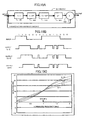
- Fig. 11A shows a graph indicating the signal attenuation with respect to the length of the wire L between the PBC and HDD.
- Fig. 11B shows the relationship between the amplitude VLf of the transmission signal of the longest wavelength, and the amplitude VHf of the transmission signal of the shortest wavelength.
- Fig. 11C shows the relationship between the amplitude VLf of the reception signal of the longest wavelength, and the amplitude VHf of the reception signal of the shortest wavelength.
- the graphs in Fig. 11 show the results of a simulation assuming that the data transfer speed is 4 Gbps. In the graph in Fig.
- the dot-dash line indicates the attenuation of a NRZ (Non Return to Zero) signal of the longest wavelength (for example, a data pattern of "11110000")
- the dotted line indicates the attenuation of a NRZ signal of the shortest wavelength (for example, a data pattern of "10101010”)
- the solid line indicates the ISI attenuation (the differential between the attenuation of the NRZ signal of the longest wavelength and the attenuation of the NRZ signal of the shortest wavelength).
- the dotted line indicates the waveform of the NRZ signal of longest wavelength
- the solid line indicates the waveform of the NRZ signal of shortest wavelength.
- "transmission signal” means a signal transmitted by the transmission circuit 17P or 17D
- “reception signal” means a signal received by the reception circuit 18P or 18D.
- the longer the length L of the wire between the PBC and the HDD the greater the ISI attenuation.
- Fig. 11B and Fig. 11C in a signal transmitted by the transmission signal 17P or 17D, there is virtually no difference between the signal amplitude VLf of the longest wavelength and the signal amplitude VHf of the shortest wavelength, but when a signal transmitted by the transmission circuit 17P or 17D is received by the reception circuit 18P or 18D, then the signal amplitude VHf at the shortest wavelength will be attenuated to a greater extent than the signal amplitude VLf at the longest wavelength. As can be seen from Fig. 11A, this becomes more pronounced, the greater the length L of the wire between the PBC and the HDD.
- the attenuation in the fiber channel signal and the ISI attenuation increase in direct proportion to at least one of the length L of the wire between the PBC and the HDD and/or the transmission frequency, and since no countermeasures are taken, the quality of the fiber channel signal declines.
- an equalizer for correcting the transmission signal in accordance with the length L of the wire between the PBC and the HDD is provided on the signal transmitter side, as shown in Fig. 12.
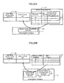
- Fig. 12 shows a general view of a first embodiment of the first mode of implementing the present invention.
- the HDD control board 20 comprises a signal correction value table 805, a board control section 815 and a boost value setting region 817.
- An equalizer (hereinafter called “PBC side equalizer”) 807 is provided in the transmission circuit 17P of the HDD control board 20, and similarly, an equalizer (hereinafter called “disk side equalizer”) 813 is provided in the transmission circuit 17D of the disk drive 4a.
- Signal correction values corresponding to the length L of the wire between the PBC and the HDD are registered in the signal correction value table 805.
- a "boost value” is one correction parameter relating to signal correction, and all of the signals transmitted or received, or a portion of these signals (such as the high-frequency signals), are boosted by means of this correction parameter.
- the boost value is, for example, a value for compensating the ISI attenuation in such a manner that the amplitude of the signal of shortest wavelength upon reception is the same as the amplitude of the signal of longest wavelength upon reception.
- the board control section 815 is a processor, such as a CPU, which takes the plurality of boost values recorded in the signal correction value table 805, and registers them in the boost value setting region 817. In this case, for example, the board control section 815 sets boost values corresponding to the disk drive installation positions, at predetermined addresses for each of the disk drive installation positions.
- the boost value setting region 817 is a storage resource (for example, a register or memory) for recording the plurality of boost values registered in the signal correction value table 805.
- the plurality of addresses in the boost value setting region 817 correspond respectively to the plurality of disk drive installation positions.
- the PBC side equalizer 807 in each of transmission circuit 17P corrects the signal on the basis of the boost value established in the boost value setting region 817 and outputs the corrected signal. More specifically, for example, the PBC side equalizer 807 boosts the level of a prescribed region of the signal (in other words, it performs signal pre-emphasis 819), on the basis of the boost value corresponding to the installation position of the disk drive 4a to which the signal is being transmitted (in other words, the boost value recorded at the address of the boost value setting region 817 corresponding to that installation position), and it then outputs the boosted signal. In this way, a boosted signal is transmitted to the disk drive 4a, via the downstream transmission path 114D.
- the PBC side equalizer 807 boosts the level of a prescribed region of the signal (in other words, it performs signal pre-emphasis 819), on the basis of the boost value corresponding to the installation position of the disk drive 4a to which the signal is being transmitted (in other words, the boost value recorded at
- the reception circuit 18D When the output signal reaches the reception circuit 18D in the disk drive 4a, it will have been attenuated in accordance with the length of the wire between the PBC and the HDD, but since the signal level was previously boosted in accordance with this length L of the wire between the PBC and the HDD, the reception circuit 18D is able to receive a signal of a suitable level.
- the reception circuit 18D may also be provided with a separate equalizer (for example, an equalizer performing de-emphasis) which corrects the received signal and then outputs this corrected signal.
- boost values are established for a disk side equalizer 813. The method for setting these boost values is described hereinafter.
- the length of the plurality of transmission paths 114D, 114U (in other words, the length L of the wire between the PBC and the HDD, for the respective disk drives 4a) varies depending on how the disk drives 4a are installed in the disk array device 1. Below, various examples of methods for installing a plurality of disk drives 4a will be described.
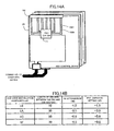
- Fig. 13A shows a general view of the front side of a plurality of disk drives 4a installed in a disk array device 1 according to a first installation method.
- Fig. 13B shows a general view of the side face of disk drives 4a installed according to a first installation method.
- Fig. 14A shows an example of the composition of a HDD control board 20 for installing disk drives 4a in accordance with a first installation method.
- the numbers contained inside each image of a disk drive 4a indicate the ID of the installation position of that disk drive 4a.
- the HDD control boards 20 are disposed at one end of a set of two or more (for example, eight) disk drives 4a arranged in the thickness direction T of the disk drives 4a (in other words, the start side or the end side in the longitudinal direction of a disk group formed by two or more disk drives 4a) . Therefore, the transmission path between each of disk drives 4a and the PBC (or switching circuit) 14 becomes longer in the direction in which the disk drive 4a are arranged. In this case, the distance between the HDD control board 20 and each of the two or more disk drives 4a (in other words, the length of the wire between the PBC and the HDD) varies significantly depending on the position at which the disk drive 4a is installed.
- the difference between the longest length L1 of the wire between the PBC and the HDD is greater than in the case of the second installation method described below.
- Fig. 14B shows examples of the values of the length L of the wire between the PBC and the HDD, the ISI attenuation, and the boost value, for respective installation positions of the disk drive 4a installed according to the first installation method. These examples relate to a case where the FC transfer speed is 4.25 Gbps. According to Fig. 14B, it can be seen that the variation in the plurality of ISI attenuation values corresponding respectively to a plurality of disk drive installation positions, (in other words, the plurality of boost values corresponding respectively to the plurality of disk drive installation positions) is greater than in the case of the second installation method described below.
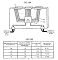
- Fig. 15A shows a general view of the front side of a plurality of disk drives 4a installed in a disk array device 1 according to a second installation method.
- Fig. 15B shows a general view of the side face of disk drives 4a installed according to a second installation method.
- Fig. 16A shows an example of the composition of a HDD control board 20 for installing disk drives 4a in accordance with a second installation method.
- the numbers contained inside each image of a disk drive 4a indicate the ID of the installation position of that disk drive 4a as in Fig. 13A.
- a disk drive group is constituted by a plurality of disk drives 4a (for example, 16 disk drives 4a) disposed in a horizontal direction, and the HDD control boards 20 are mounted in such a manner that their faces are orientated towards the side of the disk drive group, in the longitudinal direction thereof. Therefore, the transmission path between each of disk drives 4a and the PBC (or switching circuit) 14 becomes longer in a transverse direction to the direction in which the disk drives 4a are arranged (for example, the orthogonal direction) .
- the distance between the HDD control board 20 and each of the two or more disk drives 4a connected to same does not vary significantly with the position at which the disk drive 4a is installed. More specifically, for example, the difference between the longest length L1 of the wire between the PBC and the HDD (for example, the distance between the disk drive 4a at installation position ID "1F" and the rearmost HDD control board 20 of the two HDD control boards 20 connected to that disk drive 4a) and the shortest length L2 of the wire between the PBC and the HDD (for example, the distance between the disk drive 4a at installation position ID "18" and the foremost HDD control board 20 of the HDD control boards 20 connected to that disk drive 4a), is less than in the case of the first installation method described above.
- Fig. 16B shows examples of the values of the length L of the wire between the PBC and the HDD, the ISI attenuation, and the boost value, for respective installation positions of the disk drive 4a installed according to the second installation method. These examples relate to a case where the FC transfer speed is 4.25 Gbps. According to Fig. 16B, it can be seen that the variation in the plurality of ISI attenuation values corresponding respectively to a plurality of disk drive installation positions, (in other words, the plurality of boost values corresponding respectively to the plurality of disk drive installation positions) is less than in the case of the first installation method described above.
- the method for installing a plurality of disk drives 4a is not limited to these examples.
- the second installation method it may be possible to reduce the number of boost values registered in the signal correction value table 805 (see Fig. 12), compared to a case where the first installation method is adopted. This is because in the case of the second installation method, even at different disk drive installation positions, the length of the wire between the PBC and the HDD is substantially the same, and in cases of this kind, it is possible to associate one boost value with a plurality of disk drive installation positions.
- pre-emphasis can be performed by the PBC side equalizer 807 (see Fig. 12) and the disk side equalizer 813, in accordance with the length of the wire, and several pre-emphasis methods can be envisaged. Below, a number of pre-emphasis methods are described.
- Fig. 17A shows a block diagram according to a first pre-emphasis method.
- Fig. 17B shows the waveforms of the respective signals a - d in Fig. 17A.
- Fig. 17C shows graphs of amplitude against frequency, when the first pre-emphasis method is implemented.
- the PBC side equalizer 807 (or the disk side equalizer 813) according to the first pre-emphasis method is a so-called L-type equalizer, and it comprises a subtracting circuit 851, a first multiplying circuit 853, a second multiplying circuit 855, and an adding circuit 857.
- the subtracting circuit 851 performs a 1-D subtraction on the input signal a (in other words, a subtraction operation of signal a and the delay circuit D) , and it outputs the signal thus obtained.
- the first multiplying circuit 853 multiplies the signal output by the subtracting circuit 851 by a high-range correction coefficient Em for adjusting the amount of pre-emphasis, and it outputs this multiplied signal b.
- the second multiplying circuit 855 multiplies the input signal, a, by a signal amplitude coefficient K, and outputs the signal c obtained by this multiplication of signal a.
- the adding circuit 857 calculates the sum of the signal b output by the first multiplying circuit 853 and the signal c output by the second multiplying circuit 855, and it outputs this sum as signal d.
- the PBC side equalizer 807 is able to convert the input signal a into a signal d having a waveform wherein a pulse width having a period of 1 bit is added at each change point of the input signal.
- the waveform of signal d has additional 1-bit pulses at each change point in the signal, in comparison to the input signal a.
- the boost value registered in the aforementioned signal correction value table 805 is the high-range correction coefficient Em, for example.
- the transmission amplification coefficient K may be a fixed value, or it may be registered in the signal correction value table 805 with respect to each disk drive installation position.
- Fig. 18A shows a block diagram according to a second pre-emphasis method.
- Fig. 18B shows the waveforms of the respective signals a, b, c, d, e, f in Fig. 18A.
- Fig. 18C shows graphs of amplitude against frequency, when the second pre-emphasis method is implemented. Elements which are the same as those in Fig. 17A to Fig. 17C are labelled with the same reference numerals.
- the PBC side equalizer 807 (or the disk side equalizer 813) according to the second pre-emphasis method is a so-called E-type equalizer, and it comprises a first subtracting circuit 851, a second subtracting circuit 852, a first multiplying circuit 853, a third multiplying circuit 854, a second multiplying circuit 855, and an adding circuit 857.
- the first subtracting circuit 851 performs a 1-D subtraction with respect to the input signal a, and outputs the signal obtained by this subtraction operation.
- the second subtracting circuit 852 performs a 1-D -1 subtraction with respect to the input signal a, and it outputs the signal obtained by this subtraction.
- the first multiplying circuit 853 multiplies the signal output by the first subtracting circuit 851 by a high-range correction coefficient Em for adjusting the amount of pre-emphasis, and it outputs this multiplied signal b.
- the third multiplying circuit 854 multiplies the signal output by the second subtracting circuit 852 by the high-range correction coefficient Em for adjusting the amount of pre-emphasis, and it outputs this multiplied signal e.
- the second multiplying circuit 855 multiplies the input signal a by a signal amplitude coefficient K and outputs the signal c obtained by this multiplication of signal a.
- the adding circuit 857 calculates the sum of the signal b output by the first multiplying circuit 853, the signal e output by the third multiplying circuit 854, and the signal c output by the second multiplying circuit 855, and it outputs this sum as signal f.
- the PBC side equalizer 807 (or the disk side equalizer 813) according to the second pre-emphasis method performs a subtraction operation (1-D) of the data signal having passed through a 1-bit delay circuit D, and the input signal a, multiplies the signal obtained by this operation by a high-range correction coefficient Em, and then outputs the resulting signal b. Furthermore, the PBC side equalizer 807 (or disk side equalizer 813) performs a subtraction (1 - D -1 ) of the signal prior to the 1-bit delay circuit and the input signal a, multiplies the signal obtained from this operation by a high-range correction coefficient Em, and then outputs the resulting signal e.
- the PBC side equalizer 807 (or disk side equalizer 813) outputs a signal c obtained by multiplying the input signal a by a signal amplification coefficient K.
- the PBC side equalizer 807 (or disk side equalizer 813) then adds the three output signal b, e, c, together in the adding circuit 857, thereby obtaining an output waveform f wherein pulse widths having a 1-bit period are added before and after the change points in the input signal a.
- the high frequency region is emphasized more strongly than in the case of the first pre-emphasis method.
- Fig. 19A shows a block diagram according to a third pre-emphasis method.
- Fig. 19B shows an input signal waveform and output signal waveforms relating to Fig. 19A.
- Fig. 19C shows graphs of amplitude against frequency, when the third pre-emphasis method is implemented.
- the PBC side equalizer 807 (or disk side equalizer 813) according to the third pre-emphasis method is a so-called "extra-plus” type equalizer.
- the equalizer 807 (or 813) is provided with a linear digital filter, whereby pulses of 1/2 bit or less can be embedded in the "0" data in the transmission signal. Furthermore, by adjusting the coefficient Q, it is possible to adjust the waveform of the transmission signal.
- a signal correction value table 805 can be constructed in the HDD control board 20, as described below, for instance.
- Fig. 20A shows a first example of a method for constructing a signal correction value table 805.
- the management terminal 5 is one example of a computer capable of registering information in the storage region where the signal correction value table 805 is registered.
- the management terminal 5 displays a boost input value GUI (graphical user interface) 871 for inputting a boost value (dB) for each disk drive installation position.
- GUI graphical user interface
- the length L of the wire between the PBC and the HDD for each disk drive installation position is displayed on the GUI 871, so the user can tell what level of boost value to enter for each installation position.
- the user enters boost values for the respective disk drive installation positions, by means of the boost value input GUI 871.
- the management terminal 5 also comprises a boost value registering section 875.
- the boost value registering section 875 is, for example, a computer program stored in a memory, which is executed by being loaded into a CPU (not illustrated) inside the management terminal 5.
- the boost value registering section 875 registers the input boost value in the signal correction value table 805.
- the respective boost values registered in the signal correction value table 805 are values determined freely by the user.
- Fig. 20B shows a second example of a method for constructing a signal correction value table 805.
- the management terminal 5 comprises a boost value calculating section 877 in addition to the boost value registering section 875.
- the boost value calculating section 877 is, for example, a computer program stored in a memory, which is executed by being loaded into a CPU (not illustrated) inside the management terminal 5.
- the boost value calculating section 877 refers to wiring length information 874 indicating the length L of the wire between the PBC and the HDD for each installation position, and it extracts respective wire lengths and calculates boost values corresponding to the respective wire lengths thus extracted.
- the boost value registering section 875 then registers the respective boost values thus calculated in the signal correction value table 805.
- the respective boost values registered in the signal correction value table 805 are values calculated by a computer.
- boost values are established in the equalizer 807 provided in the PBC (or switching circuit 14), but boost values corresponding to the length L of the wire between the PBC and the HDD may also be established in the disk side equalizer 813.
- a computer machine for example, a management terminal 5
- a disk drive 4a installed in the disk array device 1 for example, a disk drive 4a connected to the back plane board 22
- boost values for the respective disk drives 4a may be input automatically or manually, by means of this computer machine, using either the first or second construction method described above.
- other methods such as those described below may also be envisaged.
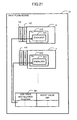
- Fig. 21 shows one example of a method for setting boost values in a disk side equalizer 813.
- a signal correction value table 881 containing boost values corresponding to respective disk drive installation positions is registered in the back plane board 22.
- the signal correction value table 881 is created in a memory, for example, and has a plurality of addresses. At each of the plurality of addresses, a boost value is stored which corresponds to the disk drive installation position (in other words, the second connector 105) associated with that address.
- the boost value located at the address corresponding to that second connector 105 (in other words, the boost value registered in the signal correction value table 881 which has been associated with the disk drive installation position corresponding to that second connector 105) is read out and established in the disk side equalizer 813 belonging to the connected disk drive 4a.
- Fig. 22 shows an example of a sequence for setting boost values for respective transmission circuits 17P, 17D, in the first embodiment.
- This sequence is an example of a case where the equalizer 807 (or 813) performs pre-emphasis according to the first or second pre-emphasis methods.
- the management terminal 5 selects a particular disk drive installation position in accordance with operations performed by the user, and it then carries out the following processing with respect to the transmission circuits 17P, 17D corresponding to that disk drive installation position.
- the management terminal 5 receives the input of a transmission amplification coefficient K which causes the amplitude of the longest wavelength signal upon reception to assume a prescribed value, and it stores the input transmission amplification coefficient K in association with the selected disk drive installation position (step S1).
- the management terminal 5 receives the input of a high-range correction coefficient Em which causes the amplitude of the shortest wavelength signal upon reception to assume the same value as the amplitude of the longest wavelength upon reception, and it stores the input high-range correction coefficient Em in association with the selected disk drive installation position (step S2).
- the management terminal 5 carries out the processing in S1 and S2, with respect to all of the disk drive installation positions (in other words, all of the transmission circuits 17P, 17D) (YES at S3), and when this has been completed, it sends the plurality of disk drive positions, the transmission amplification coefficient K values and the high-range correction coefficient Em values stored thus far, to a prescribed storage region of the HDD control board 20 or the disk drives 4a (S4).
- the management terminal 5 establishes a value for the transmission amplification coefficient K in the equalizers 807, 813 of the respective transmission circuits 17P and 17D, and it registers a high-range correction coefficient Em (boost value) in the signal correction value table 805 of the HDD control board 20.
- the value of the transmission amplification coefficient K may also be registered in the signal correction value table 805, and set in the respective equalizers 807 via the boost value setting region 817 (which is a register, for example).
- equalizers for increasing the signal amplitude were installed in the transmission circuits 17P and 17D, but equalizers of this kind may also be installed in the reception circuits 18P or 18D, or they may be installed between the transmission circuits 17P (or 17D) and the reception circuits 18D (or 18P) (for example, on the back plane board 22).
- each boost value is set on the basis of the ISI attenuation corresponding to the length of the transmission path 114U (or 114D) between the transmission circuit 17D (or reception circuit 18P) of the disk drive 4a, and the reception circuit 18P (or transmission circuit 17P) of the HDD control board 20, and the high frequency component of the signal is boosted on the basis of this boost value.
- the high frequency component of the signal is boosted on the basis of this boost value.
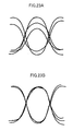
- the cross point of the eye pattern indicating the signal transmission characteristics will diverge significantly, causing the eye opening to become narrower, whereas if measures such as those described in the first embodiment are implemented, then as shown in Fig. 23B, for example, there is little divergence in the cross point of the eye pattern and the eye opening is large.
- Fig. 24 shows an example of the composition of an HDD control board 20 according to the second embodiment of the present invention.
- wavelength attribute means information relating to the wavelength of the transmitted data, for example, the data pattern.
- the board control section 815 reads out information from the signal correction value table 805 and registers it in the boost value setting region 817, and the information registered in the boost value setting region 817 is read in to each of the equalizers 807.
- a plurality of boost values, such as high-range correction coefficient values Em, are set in each of the equalizers 807.
- the equalizer 807 illustrated in Fig. 24 is one example of a so-called L-type correction circuit.
- one of the plurality of high-range correction coefficient values Em is selected on the basis of the wavelength attribute of that signal (for example, on the basis of the data pattern of the signal), and the circuit of the plurality of multiplying circuits 853 which uses the selected high-range correction coefficient Em to perform multiplication is chosen as the destination for the signal.
- a boost value is set on the basis of the ISI attenuation which corresponds to the wavelength attribute (for example, the data pattern), and the high-frequency component of the signal is boosted on the basis of that boost value.
- equalizers 807 may be applied to equalizers 807 (or 813) according to the second or third pre-emphasis methods.
- an equalizer 807 (or 813) according to this second embodiment is not limited to being provided in the transmission circuits 17P and 17D, and it may also be provided in the reception circuits 18P or 18D, or in the back plane board 22.
- boost values it is also possible to prepare values of the transmission amplification coefficient K for each wavelength attribute.
- Fig. 25A shows an example of the composition of a canister relating to a third embodiment of the first mode of implementing the present invention.
- Fig. 25B is a block diagram of the canister 4 shown in Fig. 25A.
- the canister is provided with a DC/DC connector 887, and a circuit board 891 comprising a DC/DC converter 893.
- the DC/DC connector 887 is connected to the DC/DC converter 893, and it also connects to a DC/DC connector 888 provided on the back plane board 22. If the DC/DC connector 887 is connected to the DC/DC connector 888 of the back plane board 22 (in other words, if it is powered up), then a disk identification signal, described hereinafter (for example, a signal wherein only one prescribed bit of an 8-bit signal is set to high level) is output to the circuit board 891.
- a disk identification signal described hereinafter (for example, a signal wherein only one prescribed bit of an 8-bit signal is set to high level) is output to the circuit board 891.
- the DC/DC converter 893 converts the DC voltage supplied via the DC/DC connector 887 (for example, 48V), into a DC voltage corresponding to the disk drive 4a (for example, 5V or 12V) , and it supplies this converted voltage to the disk drive 4a.
- the boost value output section 899 comprises a signal correction value table 897.
- the signal correction value table 897 registers a plurality of boost values corresponding respectively to a plurality of disk identification signals.
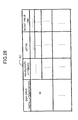
- Fig. 25C shows an example of the composition of the signal correction value table 897.
- a disk attribute and a boost value are associated with each one of a plurality of bit numbers.
- the disk attribute is an attribute relating to the disk drive 4a, and for example, it is at least one of: the type of disk drive 4a (for example, FC, SATA or SAS) , the transfer speed of the disk drive 4a, and the provider of the disk drive 4 (for example, the maker or vendor).
- the composition of the DC/DC connector 887 installed in the canister 4 (and/or the DC/DC connector 888 of the back plane board 22) varies, depending on the attribute of the disk drive 4a. For example, if there are eight types of disk attributes for the disk drive 4a, as illustrated in the example in Fig. 25C, then there are also eight types of composition for the DC/DC connector 887 (and/or 888).
- a disk identification signal according to the composition of the DC/DC connector 887 (and/or 888) is output from the DC/DC connector 887 to the boost value output section 899.
- the DC/DC connector 887 (and/or 888) of a canister 4 fitted with a disk drive 4a having a disk type of FC and a transfer speed of 4 Gbps, and whose provider is Company A outputs a disk identification signal where only the first bit is raised, to the boost value output section 899.
- the disk identification signal is also output to the HDD control board 20, via the back plane board 22.
- the boost value output section 899 receives the disk identification signal, acquires the boost value corresponding to the contents of this disk identification signal (for example, depending on which bit of the signal is raised) , from the signal correction value table 897, and outputs this boost value.
- the boost value thus output is set in the equalizer 813 of the transmission circuit 17D of the disk drive 4a, from the DC/DC connector 887, via the back plane board 22 and the connector 105.
- a suitable boost value corresponding to the disk attribute of the disk drive 4a installed in that canister 4 is automatically established in that disk drive 4a. If the reception circuit 18D is provided with an equalizer which boosts the high-frequency portion of the signal, then the boost value may be set in this equalizer in the reception circuit 18D.
- Fig. 26A shows an example of the composition of an HDD control board 20 according to the third embodiment of the present invention.
- the contents of the signal correction value table 897 provided in the HDD control board 20 are similar to those of the signal correction value table 897 provided in the canister 4.
- the boost value setting region 817 is a register, for example, and has a plurality of addresses. As shown in Fig. 26B, each of the plurality of addresses is assigned to one of a plurality of communications ports.
- a communications port is a physical or logical communications port of the PBC 14, and one communications port corresponds, for example, to one transmission circuit 17P or reception circuit 18P. Consequently, assigning an address to each of the communications ports is equivalent to assigning an address to each of the transmission circuits 17P or each of the reception circuits 18P.
- the board control section 815 is able to communicate with the management terminal 5, for example.
- the board control section 815 receives boost values to be recorded in the signal correction value table 897, from the management terminal 5, for example, and is able to write these boost values to the signal correction value table 897 in the HDD control board 20.
- the board control section 815 receives a disk identification signal from the DC/DC connector 887 of the canister 4, via the back plane board 22.
- the board control section 815 reads out a boost value corresponding to the contents of the received disk identification signal (for example, depending on which bit of the signal is raised), and it registers the boost value thus read out at a prescribed address of the boost value setting region 817.
- the address at which to register the boost value is determined according to the route via which the disk identification signal was received, for instance.
- the board control section 815 determines the storage address for the boost value in the boost value setting region 817, according to the signal path via which it received the disk identification signal, and it then registers the boost value read out as described above, at the storage address thus determined.
- the boost value registered in the boost value setting region 817 is read out to the transmission amplification control section 901 and the boost setting section 903 of each transmission circuit 17P, for example.
- the transmission amplification control section 901 regulates the value of the transmission amplification coefficient K (in other words, it regulates the amplitude of the transmission signal), on the basis of the boost value thus read out.
- the boost setting section 903 determines the high-range correction coefficient Em, on the basis of the boost value thus read out, and it sets this high-range correction coefficient value Em in the equalizer 807.
- the value of the high-range correction coefficient Em may be the same as the boost value, or it may be a different value determined on the basis of the boost value.
- a reception side equalizer 807 may be provided in the reception circuit 18P.
- This equalizer 807 may carry out prescribed correction processes, for example, performing de-emphasis with respect to the received signal (a signal which was pre-emphasized before transmission).
- Fig. 27 shows one example of a processing sequence for setting respective boost values in the boost value setting region 817, in a third embodiment of the present invention.
- the board control section 815 If a disk identification signal is received from the DC/DC connector 887 (YES at S11), then the board control section 815 reads out the boost value corresponding to the contents of the received disk identification signal, from the signal correction value table 897 (S12), and it sets the boost value thus read out in the boost value setting region 817 (S13). When this setting process has been completed, the board control section 815 sends a signal indicating that setting has been completed, to the disk drive 4a which transmitted the disk identification signal (S19). If the board control section 815 receives a response (YES at S15), then if steps S11 to S15 have not yet been carried out for all of the disk drive installation positions (NO at S16), these steps S11 to S15 are performed for the other disk drive installation positions. At S15, a response is received from the disk drive 4a when a boost value corresponding to the disk identification signal received at S11 has been set in the equalizer 813 of the disk drive 4a, for example.
- boost values corresponding to the disk attribute of the connected disk drives 4a are established in both the HDD control board 20 and the disk drives 4a, in respect of all of the disk drive installation positions.
- boost values corresponding to the disk attribute are set in the equalizers 807 and 813, and signals corrected on the basis of these boost values are transmitted. Thereby, it is possible to prevent degradation in signal quality, even if a plurality of disk drives 4a having different disk attributes are combined in the same disk array device 1.
- data is transmitted by using a boost value based on the amount of ISI attenuation corresponding to the attributes of that disk drive 4a.
- a boost value corresponding to the disk attribute of the corresponding disk drive 4a is automatically set in both the HDD control board 20 and the disk drive 4a. Accordingly, even when a canister 4 is installed in a disk array device 1, it is not necessary to perform separate tasks for setting the boost values, thus improving the convenience for the user.
- the method for detecting the disk attribute of the disk drive 4a installed in a canister 4 is not limited to the aforementioned method where a signal having a prescribed bit raised to 1 is output, depending on the composition of the DC/DC connector 887 (and/or 888), and other methods may be adopted.
- special connectors may be provided respectively on the canister 4 and on the back plane board 22, the composition of the connector provided on the canister 4 varying according to the disk attribute of the disk drive 4a installed in the canister 4.
- a signal indicating the type of special connector of the canister 4 that has been connected to the special connector of the back plane board 22 (for example, a signal indicating which of a plurality of pins in the special connector of the back plane board 22 have been connected to the connector of the canister 4) is output, and the disk attribute can be detected from this signal.
- the present invention may be implemented in various further modes.
- the plurality of equalizers 807 provided in the PBC 14 do not all have to be of the same composition, and they may also be of different compositions, depending on the size of the boost value set.
- a communications interface circuit for controlling communications between the disk drive 4a and the PBC 14 may be provided in the canister 4, and the equalizer 813 may be installed in this communications interface circuit.
- the upstream transmission path 114U and the downstream transmission path 114D may be common transmission paths.
- the signal correction value table will be a table 951 having the composition shown in Fig. 28, for instance, and hence, it will be possible to transmit data by using boost values corresponding to the ISI attenuation based on all of the following factors, namely: the disk drive installation position (in other words, the length L of the wire between the PBC and the HDD) , the wavelength attribute, and the bit number in the disk identification signal (in other words, the disk attribute).
- the boost values can be set for each port provided in the PBC 14, for example, (the ports corresponding to the transmission circuits and the ports corresponding to reception circuits).
Landscapes
- Engineering & Computer Science (AREA)
- General Engineering & Computer Science (AREA)
- Theoretical Computer Science (AREA)
- Physics & Mathematics (AREA)
- Computer Hardware Design (AREA)
- Signal Processing (AREA)
- Computer Networks & Wireless Communication (AREA)
- General Physics & Mathematics (AREA)
- Power Engineering (AREA)
- Signal Processing For Digital Recording And Reproducing (AREA)
- Optical Communication System (AREA)
- Data Exchanges In Wide-Area Networks (AREA)
- Dc Digital Transmission (AREA)
- Cable Transmission Systems, Equalization Of Radio And Reduction Of Echo (AREA)
Priority Applications (1)
| Application Number | Priority Date | Filing Date | Title |
|---|---|---|---|
| EP07001834A EP1785837A3 (de) | 2004-07-29 | 2005-04-21 | Speicherungsgerätsystem und Signalübertragungsverfahren für Speicherungsgerätsystem |
Applications Claiming Priority (1)
| Application Number | Priority Date | Filing Date | Title |
|---|---|---|---|
| JP2004222031A JP4605637B2 (ja) | 2004-07-29 | 2004-07-29 | 記憶装置システム及び記憶装置システム内での信号伝送方法 |
Related Child Applications (1)
| Application Number | Title | Priority Date | Filing Date |
|---|---|---|---|
| EP07001834A Division EP1785837A3 (de) | 2004-07-29 | 2005-04-21 | Speicherungsgerätsystem und Signalübertragungsverfahren für Speicherungsgerätsystem |
Publications (3)
| Publication Number | Publication Date |
|---|---|
| EP1622036A2 true EP1622036A2 (de) | 2006-02-01 |
| EP1622036A3 EP1622036A3 (de) | 2006-06-07 |
| EP1622036B1 EP1622036B1 (de) | 2007-12-19 |
Family
ID=34940960
Family Applications (2)
| Application Number | Title | Priority Date | Filing Date |
|---|---|---|---|
| EP07001834A Withdrawn EP1785837A3 (de) | 2004-07-29 | 2005-04-21 | Speicherungsgerätsystem und Signalübertragungsverfahren für Speicherungsgerätsystem |
| EP05252501A Expired - Lifetime EP1622036B1 (de) | 2004-07-29 | 2005-04-21 | Speicherungsgerätsystem und Signalübertragungsverfahren für Speicherungsgerätsystem |
Family Applications Before (1)
| Application Number | Title | Priority Date | Filing Date |
|---|---|---|---|
| EP07001834A Withdrawn EP1785837A3 (de) | 2004-07-29 | 2005-04-21 | Speicherungsgerätsystem und Signalübertragungsverfahren für Speicherungsgerätsystem |
Country Status (4)
| Country | Link |
|---|---|
| US (2) | US7353435B2 (de) |
| EP (2) | EP1785837A3 (de) |
| JP (1) | JP4605637B2 (de) |
| DE (1) | DE602005003880T2 (de) |
Cited By (5)
| Publication number | Priority date | Publication date | Assignee | Title |
|---|---|---|---|---|
| EP1688833A3 (de) * | 2005-02-08 | 2008-12-03 | NEC Corporation | Speichermediumarraysteuerung, Speichermediumarraygerät, Speichermediumlaufwerk, Verfahren zur Steuerung eines Speichermediumarrays und signaltragendes Medium mit integriertem Programm für eine Speichermediumarraysteuerung |
| WO2008085943A3 (en) * | 2007-01-09 | 2009-01-29 | Rambus Inc | Equalizing transmitter and method of operation |
| WO2011058603A1 (en) | 2009-11-12 | 2011-05-19 | Hitachi,Ltd. | Disk array system and hard disk drive expansion method thereof |
| EP2866135A3 (de) * | 2013-10-25 | 2015-05-06 | Samsung Electronics Co., Ltd | Serversystem und Speichersystem |
| CN105975411A (zh) * | 2016-05-11 | 2016-09-28 | 深圳市国鑫恒宇科技有限公司 | 通过固件调整磁盘柜的数据通道信号质量的方法及系统 |
Families Citing this family (16)
| Publication number | Priority date | Publication date | Assignee | Title |
|---|---|---|---|---|
| EP1662369B1 (de) * | 2004-11-30 | 2017-12-06 | Fujitsu Limited | Datenspeichersystem und Datenspeichersteuervorrichtung |
| US7877466B2 (en) * | 2005-01-11 | 2011-01-25 | Cisco Technology, Inc. | Network topology based storage allocation for virtualization |
| US20060223447A1 (en) * | 2005-03-31 | 2006-10-05 | Ali Masoomzadeh-Fard | Adaptive down bias to power changes for controlling random walk |
| US8004997B2 (en) * | 2006-03-06 | 2011-08-23 | Emulex Design & Manufacturing Corporation | Data path differentiator for pre-emphasis requirement determination or slot identification |
| JP4783709B2 (ja) * | 2006-10-18 | 2011-09-28 | 富士通株式会社 | 信号補正量設定装置、信号補正量設定方法および信号補正量設定プログラム |
| US20080168257A1 (en) * | 2007-01-05 | 2008-07-10 | Glenn Lawrence Marks | Interface assembly for coupling a host to multiple storage devices |
| WO2010146699A1 (ja) * | 2009-06-19 | 2010-12-23 | 株式会社日立製作所 | 電子計算機、電子計算機の信号補正方法 |
| JP5670624B2 (ja) * | 2009-06-25 | 2015-02-18 | アラクサラネットワークス株式会社 | 通信装置 |
| JP5342039B2 (ja) * | 2011-06-15 | 2013-11-13 | 株式会社東芝 | 電子機器 |
| US8896357B2 (en) * | 2012-05-04 | 2014-11-25 | Finisar Corporation | Integrated processor and CDR circuit |
| CN103297088B (zh) * | 2013-05-30 | 2016-08-10 | 浪潮(山东)电子信息有限公司 | 一种音频信号与485信号叠加传输的方法 |
| JP5820500B2 (ja) * | 2014-04-25 | 2015-11-24 | 株式会社日立製作所 | ディスクアレイシステム |
| US9829937B2 (en) | 2014-06-05 | 2017-11-28 | Western Digital Technologies, Inc. | Storage canister with multiple storage device mounting elements |
| US9612629B2 (en) | 2014-06-05 | 2017-04-04 | Western Digital Technologies, Inc. | Sealed storage canister |
| JP6540204B2 (ja) * | 2015-04-30 | 2019-07-10 | 富士通株式会社 | 中継装置 |
| JP7204594B2 (ja) * | 2019-06-26 | 2023-01-16 | ルネサスエレクトロニクス株式会社 | 通信システム、制御回路およびイコライザの受信信号調整方法 |
Family Cites Families (23)
| Publication number | Priority date | Publication date | Assignee | Title |
|---|---|---|---|---|
| US5412691A (en) | 1991-06-28 | 1995-05-02 | Digital Equipment Corporation | Method and apparatus for equalization for transmission over a band-limited channel |
| US6266379B1 (en) | 1997-06-20 | 2001-07-24 | Massachusetts Institute Of Technology | Digital transmitter with equalization |
| JP3638773B2 (ja) * | 1998-01-09 | 2005-04-13 | 株式会社日立製作所 | ディスクアレイ装置 |
| EP1094386A4 (de) | 1998-05-18 | 2007-05-23 | Hitachi Ltd | Speicherplattenanordnung-steuerungsvorrichtung |
| JP2000307482A (ja) | 1999-04-19 | 2000-11-02 | Fujitsu Ltd | 長距離伝送パルス送出装置 |
| JP4461511B2 (ja) | 1999-06-09 | 2010-05-12 | 株式会社日立製作所 | ディスクアレイ装置及びディスク装置へのデータ読み出し/書き込み方式 |
| US6643324B1 (en) * | 2000-05-08 | 2003-11-04 | Lsi Logic Corporation | Pad cell circuit-integrated, differential-signal equalization receiver for integrated circuit and method of boosting and equalizing high frequency differential signals |
| US6862648B2 (en) | 2000-10-30 | 2005-03-01 | Sun Microsystems, Inc. | Interface emulation for storage devices |
| US6763409B1 (en) | 2001-01-31 | 2004-07-13 | Hewlett-Packard Development Company, L.P. | Switch-on-the-fly GBIC disk channel adapter and disk channel system |
| US6850410B2 (en) | 2001-06-29 | 2005-02-01 | Emc Corporation | Advanced technology attachment disk drive module with fibre channel system characteristics |
| US7116851B2 (en) * | 2001-10-09 | 2006-10-03 | Infinera Corporation | Optical signal receiver, an associated photonic integrated circuit (RxPIC), and method improving performance |
| JP2003167796A (ja) * | 2001-11-29 | 2003-06-13 | Hitachi Ltd | ファイバーチャネルに接続されるデバイス、及びこのデバイスのマージンテスト方法、並びに、ファイバーチャネルに接続されるデバイスを有するシステムの障害部位特定方法 |
| JP3964212B2 (ja) | 2002-01-16 | 2007-08-22 | 株式会社日立製作所 | 記憶装置システム |
| US6996642B2 (en) * | 2002-04-02 | 2006-02-07 | International Business Machines Corporation | Adapter, converted data storage device and method of operation of a converted data storage device |
| JP4223256B2 (ja) * | 2002-09-25 | 2009-02-12 | 株式会社日立製作所 | ディスクアレイ装置、及びその制御方法 |
| US6826140B2 (en) * | 2002-08-26 | 2004-11-30 | Bae Systems Information And Electronic Systems Integration Inc | Multichannel digital recording system with multi-user detection |
| US7450636B2 (en) | 2002-09-05 | 2008-11-11 | Avago Technologies General Ip (Singapore) Pte. Ltd. | Adaptive transmit equalizer |
| JP2004118946A (ja) * | 2002-09-26 | 2004-04-15 | Hitachi Ltd | ディスクアレイ装置、記憶デバイスユニット、ディスクアレイ装置の制御方法、及びプログラム |
| JP4230189B2 (ja) * | 2002-10-03 | 2009-02-25 | 株式会社日立製作所 | ディスクアレイ装置、及びその電源供給方法 |
| US8234399B2 (en) | 2003-05-29 | 2012-07-31 | Seagate Technology Llc | Method and apparatus for automatic phy calibration based on negotiated link speed |
| US6975140B2 (en) | 2003-11-26 | 2005-12-13 | International Business Machines Corporation | Adaptive data transmitter having rewriteable non-volatile storage |
| JP4480386B2 (ja) * | 2003-11-28 | 2010-06-16 | 株式会社日立製作所 | ディスクアレイ装置及びディスクアレイ装置のデータ中継方法 |
| US7233164B2 (en) | 2003-12-17 | 2007-06-19 | Rambus Inc. | Offset cancellation in a multi-level signaling system |
-
2004
- 2004-07-29 JP JP2004222031A patent/JP4605637B2/ja not_active Expired - Fee Related
- 2004-09-20 US US10/943,916 patent/US7353435B2/en not_active Expired - Fee Related
-
2005
- 2005-04-21 DE DE602005003880T patent/DE602005003880T2/de not_active Expired - Lifetime
- 2005-04-21 EP EP07001834A patent/EP1785837A3/de not_active Withdrawn
- 2005-04-21 EP EP05252501A patent/EP1622036B1/de not_active Expired - Lifetime
-
2006
- 2006-11-22 US US11/603,129 patent/US7644199B2/en not_active Expired - Fee Related
Cited By (12)
| Publication number | Priority date | Publication date | Assignee | Title |
|---|---|---|---|---|
| EP1688833A3 (de) * | 2005-02-08 | 2008-12-03 | NEC Corporation | Speichermediumarraysteuerung, Speichermediumarraygerät, Speichermediumlaufwerk, Verfahren zur Steuerung eines Speichermediumarrays und signaltragendes Medium mit integriertem Programm für eine Speichermediumarraysteuerung |
| WO2008085943A3 (en) * | 2007-01-09 | 2009-01-29 | Rambus Inc | Equalizing transmitter and method of operation |
| US9148313B2 (en) | 2007-01-09 | 2015-09-29 | Rambus, Inc. | Equalizing transmitter and method of operation |
| US9749160B2 (en) | 2007-01-09 | 2017-08-29 | Rambus Inc. | Equalizing transmitter and method of operation |
| US10200220B2 (en) | 2007-01-09 | 2019-02-05 | Rambus Inc | Equalizing transmitter and method of operation |
| US10505769B2 (en) | 2007-01-09 | 2019-12-10 | Rambus Inc. | Equalizing transmitter and method of operation |
| US11121893B2 (en) | 2007-01-09 | 2021-09-14 | Rambus Inc. | Equalizing transmitter and method of operation |
| WO2011058603A1 (en) | 2009-11-12 | 2011-05-19 | Hitachi,Ltd. | Disk array system and hard disk drive expansion method thereof |
| CN102473076B (zh) * | 2009-11-12 | 2015-06-10 | 株式会社日立制作所 | 磁盘阵列系统及其硬盘驱动扩展方法 |
| EP2866135A3 (de) * | 2013-10-25 | 2015-05-06 | Samsung Electronics Co., Ltd | Serversystem und Speichersystem |
| CN105975411A (zh) * | 2016-05-11 | 2016-09-28 | 深圳市国鑫恒宇科技有限公司 | 通过固件调整磁盘柜的数据通道信号质量的方法及系统 |
| CN105975411B (zh) * | 2016-05-11 | 2019-02-12 | 深圳市同泰怡信息技术有限公司 | 通过固件调整磁盘柜的数据通道信号质量的方法及系统 |
Also Published As
| Publication number | Publication date |
|---|---|
| DE602005003880T2 (de) | 2008-12-04 |
| EP1785837A2 (de) | 2007-05-16 |
| JP2006042179A (ja) | 2006-02-09 |
| JP4605637B2 (ja) | 2011-01-05 |
| EP1785837A3 (de) | 2007-09-19 |
| US20060026336A1 (en) | 2006-02-02 |
| DE602005003880D1 (de) | 2008-01-31 |
| US7353435B2 (en) | 2008-04-01 |
| US7644199B2 (en) | 2010-01-05 |
| EP1622036A3 (de) | 2006-06-07 |
| EP1622036B1 (de) | 2007-12-19 |
| US20070064132A1 (en) | 2007-03-22 |
Similar Documents
| Publication | Publication Date | Title |
|---|---|---|
| EP1622036B1 (de) | Speicherungsgerätsystem und Signalübertragungsverfahren für Speicherungsgerätsystem | |
| KR101039172B1 (ko) | 와이드 포트를 갖는 저장 서브시스템에서의 케이블 길이를 검출하기 위한 장치 및 방법 | |
| US8767768B2 (en) | Data path differentiator for pre-emphasis requirement or slot identification | |
| CN102332667B (zh) | 用于有源电缆的电路 | |
| US20110267073A1 (en) | Validating high speed link performance margin for switch fabric with any-to-any connection across a midplane | |
| US10229081B2 (en) | System level crosstalk mitigation | |
| US20230345620A1 (en) | Hatching ground under a pad in a printed circuit board | |
| CN120378390B (zh) | 网卡连接电路和服务器 | |
| CN101667991B (zh) | 一种设置预加重和/或均衡参数的方法及装置 | |
| US7284073B2 (en) | Disk array apparatus and data relay method of the disk array apparatus | |
| US20220158877A1 (en) | Interconnect module, ufs system including the same, and method of operating the ufs system | |
| US6970054B2 (en) | Apparatus for terminating transmission lines to reduce electromagnetic interference in an electronic system | |
| US20230061937A1 (en) | Adaptive module port and circuitry | |
| US20050025307A1 (en) | Configurable communications modules and methods of making the same | |
| US7852781B1 (en) | Managing communications settings | |
| US20040066095A1 (en) | Apparatus for controlling transmissions to reduce electromagnetic interference in an electronic system | |
| US20090245395A1 (en) | Transmission control apparatus and transmission control method | |
| US20230342321A1 (en) | Enhanced eye-width margin using duty cycle adjust | |
| TWI894647B (zh) | 依不同熱源資訊進行訊號最佳化調整之系統與方法 | |
| Hughes et al. | BladeCenter midplane and media interface card | |
| US9294317B1 (en) | Equalizer-compensated AC-coupled termination | |
| de Araujo et al. | Complex high speed links in server environments | |
| HK1094363B (en) | A storage medium array controller, a storage medium array apparatus, a storage medium drive, a method of controlling a storage medium array, and a signal-bearing medium embodying a program of a storage medium array controller | |
| HK1094363A1 (en) | A storage medium array controller, a storage medium array apparatus, a storage medium drive, a method of controlling a storage medium array, and a signal-bearing medium embodying a program of a storage medium array controller |
Legal Events
| Date | Code | Title | Description |
|---|---|---|---|
| PUAI | Public reference made under article 153(3) epc to a published international application that has entered the european phase |
Free format text: ORIGINAL CODE: 0009012 |
|
| 17P | Request for examination filed |
Effective date: 20050510 |
|
| AK | Designated contracting states |
Kind code of ref document: A2 Designated state(s): AT BE BG CH CY CZ DE DK EE ES FI FR GB GR HU IE IS IT LI LT LU MC NL PL PT RO SE SI SK TR |
|
| AX | Request for extension of the european patent |
Extension state: AL BA HR LV MK YU |
|
| PUAL | Search report despatched |
Free format text: ORIGINAL CODE: 0009013 |
|
| AK | Designated contracting states |
Kind code of ref document: A3 Designated state(s): AT BE BG CH CY CZ DE DK EE ES FI FR GB GR HU IE IS IT LI LT LU MC NL PL PT RO SE SI SK TR |
|
| AX | Request for extension of the european patent |
Extension state: AL BA HR LV MK YU |
|
| 17Q | First examination report despatched |
Effective date: 20060904 |
|
| AKX | Designation fees paid |
Designated state(s): DE FR GB |
|
| GRAP | Despatch of communication of intention to grant a patent |
Free format text: ORIGINAL CODE: EPIDOSNIGR1 |
|
| GRAS | Grant fee paid |
Free format text: ORIGINAL CODE: EPIDOSNIGR3 |
|
| GRAA | (expected) grant |
Free format text: ORIGINAL CODE: 0009210 |
|
| AK | Designated contracting states |
Kind code of ref document: B1 Designated state(s): DE FR GB |
|
| REG | Reference to a national code |
Ref country code: GB Ref legal event code: FG4D |
|
| REF | Corresponds to: |
Ref document number: 602005003880 Country of ref document: DE Date of ref document: 20080131 Kind code of ref document: P |
|
| ET | Fr: translation filed | ||
| PLBE | No opposition filed within time limit |
Free format text: ORIGINAL CODE: 0009261 |
|
| STAA | Information on the status of an ep patent application or granted ep patent |
Free format text: STATUS: NO OPPOSITION FILED WITHIN TIME LIMIT |
|
| 26N | No opposition filed |
Effective date: 20080922 |
|
| PGFP | Annual fee paid to national office [announced via postgrant information from national office to epo] |
Ref country code: FR Payment date: 20090309 Year of fee payment: 5 |
|
| REG | Reference to a national code |
Ref country code: FR Ref legal event code: ST Effective date: 20101230 |
|
| PG25 | Lapsed in a contracting state [announced via postgrant information from national office to epo] |
Ref country code: FR Free format text: LAPSE BECAUSE OF NON-PAYMENT OF DUE FEES Effective date: 20100430 |
|
| PGFP | Annual fee paid to national office [announced via postgrant information from national office to epo] |
Ref country code: DE Payment date: 20200408 Year of fee payment: 16 |
|
| PGFP | Annual fee paid to national office [announced via postgrant information from national office to epo] |
Ref country code: GB Payment date: 20200408 Year of fee payment: 16 |
|
| REG | Reference to a national code |
Ref country code: DE Ref legal event code: R119 Ref document number: 602005003880 Country of ref document: DE |
|
| GBPC | Gb: european patent ceased through non-payment of renewal fee |
Effective date: 20210421 |
|
| PG25 | Lapsed in a contracting state [announced via postgrant information from national office to epo] |
Ref country code: DE Free format text: LAPSE BECAUSE OF NON-PAYMENT OF DUE FEES Effective date: 20211103 Ref country code: GB Free format text: LAPSE BECAUSE OF NON-PAYMENT OF DUE FEES Effective date: 20210421 |