EP1624492A2 - Détecteur d'image à dispositif couplé de charge à phase virtuelle - Google Patents
Détecteur d'image à dispositif couplé de charge à phase virtuelle Download PDFInfo
- Publication number
- EP1624492A2 EP1624492A2 EP04103751A EP04103751A EP1624492A2 EP 1624492 A2 EP1624492 A2 EP 1624492A2 EP 04103751 A EP04103751 A EP 04103751A EP 04103751 A EP04103751 A EP 04103751A EP 1624492 A2 EP1624492 A2 EP 1624492A2
- Authority
- EP
- European Patent Office
- Prior art keywords
- charge
- clocked
- gate
- clocking signal
- region
- Prior art date
- Legal status (The legal status is an assumption and is not a legal conclusion. Google has not performed a legal analysis and makes no representation as to the accuracy of the status listed.)
- Withdrawn
Links
Images


Classifications
-
- H—ELECTRICITY
- H10—SEMICONDUCTOR DEVICES; ELECTRIC SOLID-STATE DEVICES NOT OTHERWISE PROVIDED FOR
- H10F—INORGANIC SEMICONDUCTOR DEVICES SENSITIVE TO INFRARED RADIATION, LIGHT, ELECTROMAGNETIC RADIATION OF SHORTER WAVELENGTH OR CORPUSCULAR RADIATION
- H10F39/00—Integrated devices, or assemblies of multiple devices, comprising at least one element covered by group H10F30/00, e.g. radiation detectors comprising photodiode arrays
- H10F39/10—Integrated devices
- H10F39/12—Image sensors
- H10F39/15—Charge-coupled device [CCD] image sensors
- H10F39/158—Charge-coupled device [CCD] image sensors having arrangements for blooming suppression
-
- H—ELECTRICITY
- H10—SEMICONDUCTOR DEVICES; ELECTRIC SOLID-STATE DEVICES NOT OTHERWISE PROVIDED FOR
- H10F—INORGANIC SEMICONDUCTOR DEVICES SENSITIVE TO INFRARED RADIATION, LIGHT, ELECTROMAGNETIC RADIATION OF SHORTER WAVELENGTH OR CORPUSCULAR RADIATION
- H10F39/00—Integrated devices, or assemblies of multiple devices, comprising at least one element covered by group H10F30/00, e.g. radiation detectors comprising photodiode arrays
- H10F39/10—Integrated devices
- H10F39/12—Image sensors
- H10F39/15—Charge-coupled device [CCD] image sensors
- H10F39/153—Two-dimensional or three-dimensional array CCD image sensors
- H10F39/1536—Frame transfer
-
- H—ELECTRICITY
- H10—SEMICONDUCTOR DEVICES; ELECTRIC SOLID-STATE DEVICES NOT OTHERWISE PROVIDED FOR
- H10F—INORGANIC SEMICONDUCTOR DEVICES SENSITIVE TO INFRARED RADIATION, LIGHT, ELECTROMAGNETIC RADIATION OF SHORTER WAVELENGTH OR CORPUSCULAR RADIATION
- H10F39/00—Integrated devices, or assemblies of multiple devices, comprising at least one element covered by group H10F30/00, e.g. radiation detectors comprising photodiode arrays
- H10F39/80—Constructional details of image sensors
Definitions
- the present invention relates to solid-state image sensors and specifically to a class of Virtual Phase (VP) charge coupled device (CCD) image sensors that have high sensitivity, high blue response, low smear, and that multiply collected charge using single carrier impact ionization process before charge conversion into a voltage.
- VP Virtual Phase
- CCD charge coupled device
- a typical image sensor senses light by converting impinging photons into electrons that are integrated (collected) in the image sensing area array of pixels. After completion of integration collected electrons are transported into a suitable storage area by the CCD transfer process and further from the storage area into the detection node where electron charge is converted into a voltage. The resulting voltage is then supplied to the output terminals of the sensor.
- FF Full Frame
- FT Frame Transfer
- FIT Frame Interline Transfer
- charge is first integrated in special photo sites, which are not located directly in column registers of the image sensing area array as in the FF and FT devices. After the integration cycle is completed charge from the photo-sites is transferred into the column registers that are shielded from impinging light and then further into the storage area.
- FF image sensors The image sensors that do not have memory area and use a mechanical shutter to block off light during the readout that is performed directly from the image sensing area are called FF image sensors. All three types of the sensor architectures, FF, FT, and FIT, can be built using the VP technology. The detail description of this technology can be found in US patent 4,229,752 to Hynecek. While the VP technology has significant advantages in using fewer clock lines for charge transport and in having high Quantum Efficiency (QE), it has a problem of generating a small amount of clock induced spurious charge dark current.
- QE Quantum Efficiency
- FIG. 4 is a schematic drawing of a top view of a CCD register that is using the two-phase gate structure surrounded by field plate of FIG. 3.
- the drawing shows the detail of the serial register that interfaces with the image storage area.
- the drawing also shows the detail of the charge overflow barrier and the serial register anti-blooming drain;
- FIG. 5 is a schematic drawing of a top view of a CCD register that is using the two-phase gate structure surrounded by field plate of FIG. 3.
- the drawing shows the detail of the register that does not interface with the image memory area and that may also be used for charge multiplication.
- the drawing shows the charge overflow barrier and the serial register anti-blooming drain;
- FIG. 6 is a schematic drawing of a top view of a CCD register in the image sensing area of the VP FIT CCD sensor.
- the drawing shows the photo-site region for collection of photo-charge, which has a lateral anti-blooming barrier with anti-blooming drain for collection of excess charge.
- the drawing also shows the detail of the column CCD channel that is used for fast transfer of charge into the image memory area;
- FIG. 7 is a schematic drawing of a timing chart that shows the detail of the charge transfer pulse that causes transfer of collected charge from the photo-sites of the VP FIT CCD image sensor into the column registers and the subsequent pulse sequence that causes transfer of photo-charge into the image memory area.
- the drawing 100 represents simplified cross section through the middle of the CCD channel of a standard prior art VP CCD device together with corresponding channel potential profiles in various device sections for the high and low gate biasing levels.
- P-type substrate 101 has n-type buried channel implant 102 near its surface.
- Oxide layer 104 separates the substrate from poly silicon gate electrodes 105 that are connected together and to a bias terminal by metal wiring 106.
- P+ type Virtual Phase implant 103 has been implanted between gate electrodes 105. The directionality of charge transfer is created by placing additional implants 107 and 108 near the surface of the substrate just under poly gate electrodes 105 and VP gate region 103.
- the resulting structure after depletion of excess mobile charge, creates potential profile in each pixel described by segments 116, 112, 119, 110, 115, and 116, for low gate biasing level and by segments 116, 113, 114, 111, 115, and 116, for high gate biasing level.
- Charge packet 118 which has been stored in well 111, is transferred to level 110 when a low bias is applied to gates 105 and flows to well 116 where it becomes charge packet 117.
- charge packet 117 from well 116 flows to well 111, where it becomes charge packet 118.
- charge packets are transported along the CCD register from image area pixels to the memory area pixels and from the memory area pixels through the serial register to the charge detection node for final detection and conversion to output voltage.
- This is well known to all those skilled in the art and will not be discussed here in any further detail.
- the important point to note, however, is the collapse of the well potential step 114 when the poly-silicon gate bias transitions from high to low.
- the step 114 is significantly reduced to a smaller step 119.
- the potential step reduction is advantageous for reduction of the gate clocking voltage amplitude and for improvement of Charge Transfer Efficiency (CTE).
- CTE Charge Transfer Efficiency
- the potential step reduction is a consequence of accumulation of holes at the silicon-silicon dioxide interface under poly-silicon gates 105.
- more complicated double layer poly-silicon gate electrodes 205 and 208 have replaced single layer poly-silicon gate electrodes 105.
- regions 201 through 207 correspond to identical regions 101 through 107 in drawing 100.
- Gate electrodes 208, called Clocked Barrier electrodes, are connected together and to the bias terminal by metal wiring 209 similarly as gate electrodes 205 are connected together and to the bias terminal by metal wiring 206.
- Resulting potential profile that is created in silicon substrate 201 by the new poly-silicon gate structure 205 and 208 is similar to the previous potential profile shown in drawing 100.
- Potential profile segments and the electron charge transport shown in drawing 200 indicated by numbers 210 through 219 correspond to identical potential profile segments and the electron charge transfer indicated by numbers 110 through 119 in drawing 100.
- potential levels 212 and 213 are controlled independently from levels 210 and 211 by applying separate and different clock biases to gates 205 and 208.
- the clocking bias applied to gates 205 is in phase with the clocking bias applied to gates 208.
- This allows the desired smaller potential step 219 without accumulation of holes.
- By preventing accumulation of holes at the silicon-silicon dioxide interface during clocking eliminates generation of unwanted clocking induced dark current. This significantly improves low light level performance of these devices while maintaining all other advantages of VP CCD technology.
- CB Clocked Barrier
- P-type doped silicon substrate 301 has n-type doped buried layer 302 near its surface.
- Oxide layer 304 on top of the silicon surface separates substrate 301 from poly-silicon gates 305, 307, and 309.
- the first deposited layer of poly-silicon forms field plate gates 305, which are connected using metal wiring 306 to bias terminal.
- the second poly-silicon layer separated form the first one by an oxide dielectric layer, forms separate and independently biased gate electrodes 307 and 309, which are also connected using respective metal wirings 308 and 310 to corresponding bias terminals.
- the field plate is used to create a suitable potential profile that confines charge in the direction perpendicular to the plane of the drawing without the necessity for heavily doped p+ channel stops. This eliminates the source of unwanted clocking induced dark current caused by impact ionization within such channel stops.
- the second advantage is a better control of potential profile when this pixel structure is used in charge multiplying registers and the charge-multiplying gate needs to be biased to high biasing levels necessary for the onset of electron multiplication.
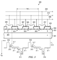
- FIG. 4 simplified drawing 400 of an example of one possible layout embodiment is shown in FIG. 4.
- Drawing 400 also shows the details of the interface region between the CCD memory area and serial register.
- the memory area consists of CCD columns separated by p+ doped channel stops 401.
- a conventional VP CCD gate structure 403 is shown with barrier region 405 and well region 404.
- the new CB VP CCD structure, shown in drawing 200 can easily be substituted here as is clear to all those skilled in the art.
- Gate 403 interfaces with virtual well region 402 and virtual barrier region 406 that further interfaces with field plate region 407 of the serial register.
- Field plate region 407 formed from the fist poly-silicon layer, has openings 415 and notches 413 that are overlaid by the second poly-silicon layer, which forms gates 409 and 410.
- Metal wirings 408, 411, and 412 serve as interconnects between gates, the field plate, and the biasing terminals.
- Charge flow directionality is established by implanting barrier regions 414 and 416 under gates 409 and 410.
- Charge that is transferred from memory area into the serial register flows from Virtual Barrier region 406 under field plate region 422 and further under gate 409. Charge is confined to stay in these regions by suitable potential barrier forming implants 417 and 418 that have replaced the traditional p+ channel stops used in conventional designs.
- gates 409 and 410 which transport charge in serial register do not overlap any p+ channel stop anywhere. This eliminates generation of spurious clocking induced dark current even for high biases required for the onset of charge multiplication.
- An important feature introduced in this design is the serial register blooming protection. This is accomplished by incorporating anti-blooming barrier implants 421 under gates 409. When a large amount of charge accumulates under these gates, either from excessive charge multiplication in charge multiplying sections of the register or from summing of several lines of data transferred from the memory into the register, excess charge can harmlessly overflow into drain 419 without corrupting charge signal under neighboring gates 410.
- Overflow charge collecting drain 419 is connected to biasing terminal by wiring 420. The drain interfaces with active device border 423.
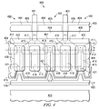
- FIG. 5 When the serial register does not interface with the sensor imaging or memory areas, another peripheral charge collecting drain can be placed next to it. This is shown in drawing 500 in FIG. 5.
- features 507 through 523 correspond to identical features 407 through 423 shown in drawing 400.
- the only differences are in the shape of the charge confining potential barrier implant 517 that is now contiguous and runs continuously along the length of the register.
- the second difference is in elimination of region that would be equivalent to region 422. This region is not needed here, since no charge is being transferred into the serial register in parallel direction.
- Peripheral charge collecting drain 524 is connected to appropriate biasing terminal by wiring 525. The drain also interfaces with the border of the device active region 523.
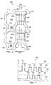
- Drawing 600 in FIG. 6 is a simplified design layout of FIT image sensing area pixel.
- Region 601 is the p+ type doped channel-stop that delineates the boundary of each pixel.
- the pixels consist of photo-site regions 604 that may be formed by n+ type doped regions or by pinned (buried) photo-diodes similar to region 103.
- Photo-diode 604 also interfaces with anti-blooming barrier 605 and anti-blooming drain 606.
- Anti-blooming barrier and drain remove excessive charge from the pixels to prevent corruption of charge data that is transported in column CCD channels 610.
- Metal wiring connections and contact regions to supply bias to anti-blooming drains were for simplicity omitted from the drawing.
- Transfer of charge from photo-diode into column channel 610 is activated when a suitable pulse is applied to gate 602.
- This gate may be formed from the first poly-silicon layer.
- the second poly-silicon layer may be used to form CB gate 603.
- the gate metal interconnection wiring 611 and 612 with corresponding contact regions are shown in the drawing only schematically.
- the photo-site light shield which usually covers the column CCD channels, is omitted from the drawing.
- the virtual phase region is formed by virtual barrier region 607 and virtual well region 608. To prevent charge flow from photo-site region 604 to CCD register 610, when charge is being transported in column CCD channels 610, suitable charge transfer potential barrier forming implant 609 has been paced under poly-silicon gate 602.
- the FIT sensor that uses above described pixels in its image sensing area array for charge sensing operates as follows: after completion of integrating period, collected charge from photo-sites 604 is transferred to column CCD registers 610 by using a special pulse applied to gates 602. After completion of this pulse timing interval, charge is transferred in column CCD registers 610 into the memory area array, which is adjacent to the image sensing area. The charge transfer in the columns 610 is accomplished by applying standard clocking pulses to gates 603 and 602.
- FIG. 7 a simplified timing diagram 700 is shown in FIG 7.
- Special pulse 701 that has higher amplitude than standard, and which is being pulsed between levels 706 and 704, accomplishes the photo-site charge transfer. This pulse is applied only to gates 602.
- the charge transfer within registers 610 is accomplished by applying pulses 703 to gates 603 together with pulses 702 applied to gates 602.
- Pulses 702 and 703 have standard amplitudes and are being pulsed between levels 708 and 707 for pulses 703 and between levels 706 and 705 for pulses 702.
- Levels 706 and 708 may have identical bias voltages.
- Levels 707 and 705 may also have identical bias voltages although different than levels 706 and 708.
- the architectures of the described devices are based on the FF, FT, and on the FIT concepts.
- the small amount of clocked induced dark current, usually present in VP CCD devices, is eliminated in these devices by designing the CB pixel architecture for the image and memory area pixels and a special two-phase gate structure surrounded by field plate for the pixels of the serial and charge multiplication registers.
Landscapes
- Solid State Image Pick-Up Elements (AREA)
- Transforming Light Signals Into Electric Signals (AREA)
Applications Claiming Priority (1)
| Application Number | Priority Date | Filing Date | Title |
|---|---|---|---|
| US10/633,993 US20050029553A1 (en) | 2003-08-04 | 2003-08-04 | Clocked barrier virtual phase charge coupled device image sensor |
Publications (2)
| Publication Number | Publication Date |
|---|---|
| EP1624492A2 true EP1624492A2 (fr) | 2006-02-08 |
| EP1624492A3 EP1624492A3 (fr) | 2006-06-07 |
Family
ID=34115956
Family Applications (1)
| Application Number | Title | Priority Date | Filing Date |
|---|---|---|---|
| EP04103751A Withdrawn EP1624492A3 (fr) | 2003-08-04 | 2004-08-04 | Détecteur d'image à dispositif couplé de charge à phase virtuelle |
Country Status (3)
| Country | Link |
|---|---|
| US (1) | US20050029553A1 (fr) |
| EP (1) | EP1624492A3 (fr) |
| JP (1) | JP2005057772A (fr) |
Families Citing this family (14)
| Publication number | Priority date | Publication date | Assignee | Title |
|---|---|---|---|---|
| GB2413007A (en) * | 2004-04-07 | 2005-10-12 | E2V Tech Uk Ltd | Multiplication register for amplifying signal charge |
| US7719036B2 (en) * | 2005-09-02 | 2010-05-18 | Imagerlabs, Inc. | Charge coupled device with high quantum efficiency |
| JP4612518B2 (ja) * | 2005-10-07 | 2011-01-12 | 株式会社日立国際電気 | 電子増倍型撮像装置およびその感度調整方法 |
| US7485840B2 (en) * | 2007-02-08 | 2009-02-03 | Dalsa Corporation | Semiconductor charge multiplication amplifier device and semiconductor image sensor provided with such an amplifier device |
| US20110073982A1 (en) * | 2007-05-25 | 2011-03-31 | Armstrong J Joseph | Inspection system using back side illuminated linear sensor |
| JP5237843B2 (ja) * | 2009-01-30 | 2013-07-17 | 浜松ホトニクス株式会社 | 固体撮像装置 |
| JP5270392B2 (ja) * | 2009-01-30 | 2013-08-21 | 浜松ホトニクス株式会社 | 固体撮像装置 |
| JP5243984B2 (ja) * | 2009-01-30 | 2013-07-24 | 浜松ホトニクス株式会社 | 電子増倍機能内蔵型の固体撮像素子 |
| JP5330001B2 (ja) * | 2009-01-30 | 2013-10-30 | 浜松ホトニクス株式会社 | 固体撮像装置 |
| JP5243983B2 (ja) * | 2009-01-30 | 2013-07-24 | 浜松ホトニクス株式会社 | 電子増倍機能内蔵型の固体撮像素子 |
| JP5335459B2 (ja) * | 2009-01-30 | 2013-11-06 | 浜松ホトニクス株式会社 | 電子増倍機能内蔵型の固体撮像素子 |
| FR2945667B1 (fr) * | 2009-05-14 | 2011-12-16 | Commissariat Energie Atomique | Capteur d'image integre a tres grande sensibilite. |
| FR2945668B1 (fr) * | 2009-05-14 | 2011-12-16 | Commissariat Energie Atomique | Capteur d'image pour imagerie a tres bas niveau de lumiere. |
| US8847285B2 (en) | 2011-09-26 | 2014-09-30 | Semiconductor Components Industries, Llc | Depleted charge-multiplying CCD image sensor |
Family Cites Families (15)
| Publication number | Priority date | Publication date | Assignee | Title |
|---|---|---|---|---|
| US4173064A (en) * | 1977-08-22 | 1979-11-06 | Texas Instruments Incorporated | Split gate electrode, self-aligned antiblooming structure and method of making same |
| US4229752A (en) * | 1978-05-16 | 1980-10-21 | Texas Instruments Incorporated | Virtual phase charge transfer device |
| US4857979A (en) * | 1988-06-20 | 1989-08-15 | Ford Aerospace & Communications Corporation | Platinum silicide imager |
| KR100298039B1 (ko) * | 1991-07-11 | 2001-10-24 | 윌리엄 비. 켐플러 | 전하증배장치및그제조방법 |
| JP3227808B2 (ja) * | 1992-07-21 | 2001-11-12 | ソニー株式会社 | Fit型固体撮像装置 |
| DE69410147T2 (de) * | 1993-03-03 | 1998-12-03 | Philips Electronics N.V., Eindhoven | Ladungsgekoppelte Anordnung |
| US5502318A (en) * | 1994-02-14 | 1996-03-26 | Texas Instruments Incorporated | Bipolar gate charge coupled device with clocked virtual phase |
| US5430481A (en) * | 1994-03-30 | 1995-07-04 | Texas Instruments Incorporated | Multimode frame transfer image sensor |
| JPH09191101A (ja) * | 1996-01-09 | 1997-07-22 | Sony Corp | 電荷転送装置およびこれを用いた固体撮像装置 |
| DE19854915C2 (de) * | 1998-11-27 | 2002-09-05 | Infineon Technologies Ag | MOS-Feldeffekttransistor mit Hilfselektrode |
| US6278142B1 (en) * | 1999-08-30 | 2001-08-21 | Isetex, Inc | Semiconductor image intensifier |
| US6680222B2 (en) * | 1999-11-05 | 2004-01-20 | Isetex, Inc | Split-gate virtual-phase CCD image sensor with a diffused lateral overflow anti-blooming drain structure and process of making |
| US6218692B1 (en) * | 1999-11-23 | 2001-04-17 | Eastman Kodak Company | Color active pixel sensor with electronic shuttering, anti-blooming and low cross talk |
| US20010031517A1 (en) * | 1999-12-28 | 2001-10-18 | Jaroslav Hynecek | Process for fabrication of split-gate virtual phase charge coupled devices |
| JP4635291B2 (ja) * | 2000-03-31 | 2011-02-23 | 日本テキサス・インスツルメンツ株式会社 | 半導体装置の製造方法 |
-
2003
- 2003-08-04 US US10/633,993 patent/US20050029553A1/en not_active Abandoned
-
2004
- 2004-08-03 JP JP2004226558A patent/JP2005057772A/ja active Pending
- 2004-08-04 EP EP04103751A patent/EP1624492A3/fr not_active Withdrawn
Also Published As
| Publication number | Publication date |
|---|---|
| JP2005057772A (ja) | 2005-03-03 |
| EP1624492A3 (fr) | 2006-06-07 |
| US20050029553A1 (en) | 2005-02-10 |
Similar Documents
| Publication | Publication Date | Title |
|---|---|---|
| US12133006B2 (en) | Solid-state imaging device and imaging system | |
| US6278142B1 (en) | Semiconductor image intensifier | |
| KR970007711B1 (ko) | 오버-플로우 드레인(ofd)구조를 가지는 전하결합소자형 고체촬상장치 | |
| EP0854516B1 (fr) | Photodiode de type à couche partiellement attachée pour capteurs d'images à l'état solide | |
| US8471315B1 (en) | CMOS image sensor having global shutter pixels built using a buried channel transfer gate with a surface channel dark current drain | |
| US4168444A (en) | Imaging devices | |
| US7265397B1 (en) | CCD imager constructed with CMOS fabrication techniques and back illuminated imager with improved light capture | |
| JPH0271532A (ja) | 高ダイナミックレンジ電荷結合装置 | |
| JPS5819080A (ja) | 固体撮像素子 | |
| EP1624492A2 (fr) | Détecteur d'image à dispositif couplé de charge à phase virtuelle | |
| US9966399B2 (en) | Pixel having a plurality of pinned photodiodes | |
| US9117729B2 (en) | Depleted charge-multiplying CCD image sensor | |
| EP1850387B1 (fr) | Dispositif de capture d'images a semi-conducteurs | |
| US5703642A (en) | Full depletion mode clocking of solid-state image sensors for improved MTF performance | |
| US5256891A (en) | CCD electrode structure for image sensors | |
| US5774182A (en) | Solid-state image sensor device with pixel array structure of interline transfer CCD image sensor | |
| US7804113B2 (en) | Anti-blooming structures for back-illuminated imagers | |
| US20070278535A1 (en) | Solid-state imaging device and imaging apparatus | |
| JP4493124B2 (ja) | 固体撮像装置 | |
| JP4824241B2 (ja) | 半導体エネルギー検出器 | |
| JP4751846B2 (ja) | Ccd固体撮像素子 | |
| JP2006210680A (ja) | 固体撮像素子 | |
| EP3082165A1 (fr) | Pixel ayant une pluralité de photodiodes | |
| KR100271804B1 (ko) | 고체촬상소자 및 그 구동방법 | |
| KR100269636B1 (ko) | 고체촬상소자 |
Legal Events
| Date | Code | Title | Description |
|---|---|---|---|
| PUAI | Public reference made under article 153(3) epc to a published international application that has entered the european phase |
Free format text: ORIGINAL CODE: 0009012 |
|
| AK | Designated contracting states |
Kind code of ref document: A2 Designated state(s): AT BE BG CH CY CZ DE DK EE ES FI FR GB GR HU IE IT LI LU MC NL PL PT RO SE SI SK TR |
|
| AX | Request for extension of the european patent |
Extension state: AL HR LT LV MK |
|
| PUAL | Search report despatched |
Free format text: ORIGINAL CODE: 0009013 |
|
| AK | Designated contracting states |
Kind code of ref document: A3 Designated state(s): AT BE BG CH CY CZ DE DK EE ES FI FR GB GR HU IE IT LI LU MC NL PL PT RO SE SI SK TR |
|
| AX | Request for extension of the european patent |
Extension state: AL HR LT LV MK |
|
| AKX | Designation fees paid | ||
| REG | Reference to a national code |
Ref country code: DE Ref legal event code: 8566 |
|
| STAA | Information on the status of an ep patent application or granted ep patent |
Free format text: STATUS: THE APPLICATION IS DEEMED TO BE WITHDRAWN |
|
| 18D | Application deemed to be withdrawn |
Effective date: 20061208 |