EP1628468A2 - Dispositif de prise d'images à l'état solide et appareil de prise d'images - Google Patents
Dispositif de prise d'images à l'état solide et appareil de prise d'images Download PDFInfo
- Publication number
- EP1628468A2 EP1628468A2 EP05017430A EP05017430A EP1628468A2 EP 1628468 A2 EP1628468 A2 EP 1628468A2 EP 05017430 A EP05017430 A EP 05017430A EP 05017430 A EP05017430 A EP 05017430A EP 1628468 A2 EP1628468 A2 EP 1628468A2
- Authority
- EP
- European Patent Office
- Prior art keywords
- conversion elements
- photoelectric conversion
- dimensional array
- voltage
- sharing
- Prior art date
- Legal status (The legal status is an assumption and is not a legal conclusion. Google has not performed a legal analysis and makes no representation as to the accuracy of the status listed.)
- Granted
Links
Images





Classifications
-
- H—ELECTRICITY
- H10—SEMICONDUCTOR DEVICES; ELECTRIC SOLID-STATE DEVICES NOT OTHERWISE PROVIDED FOR
- H10F—INORGANIC SEMICONDUCTOR DEVICES SENSITIVE TO INFRARED RADIATION, LIGHT, ELECTROMAGNETIC RADIATION OF SHORTER WAVELENGTH OR CORPUSCULAR RADIATION
- H10F39/00—Integrated devices, or assemblies of multiple devices, comprising at least one element covered by group H10F30/00, e.g. radiation detectors comprising photodiode arrays
- H10F39/10—Integrated devices
- H10F39/12—Image sensors
-
- H—ELECTRICITY
- H04—ELECTRIC COMMUNICATION TECHNIQUE
- H04N—PICTORIAL COMMUNICATION, e.g. TELEVISION
- H04N25/00—Circuitry of solid-state image sensors [SSIS]; Control thereof
- H04N25/40—Extracting pixel data from image sensors by controlling scanning circuits, e.g. by modifying the number of pixels sampled or to be sampled
- H04N25/46—Extracting pixel data from image sensors by controlling scanning circuits, e.g. by modifying the number of pixels sampled or to be sampled by combining or binning pixels
-
- H—ELECTRICITY
- H04—ELECTRIC COMMUNICATION TECHNIQUE
- H04N—PICTORIAL COMMUNICATION, e.g. TELEVISION
- H04N25/00—Circuitry of solid-state image sensors [SSIS]; Control thereof
- H04N25/70—SSIS architectures; Circuits associated therewith
- H04N25/76—Addressed sensors, e.g. MOS or CMOS sensors
- H04N25/77—Pixel circuitry, e.g. memories, A/D converters, pixel amplifiers, shared circuits or shared components
-
- H—ELECTRICITY
- H04—ELECTRIC COMMUNICATION TECHNIQUE
- H04N—PICTORIAL COMMUNICATION, e.g. TELEVISION
- H04N25/00—Circuitry of solid-state image sensors [SSIS]; Control thereof
- H04N25/70—SSIS architectures; Circuits associated therewith
- H04N25/76—Addressed sensors, e.g. MOS or CMOS sensors
- H04N25/77—Pixel circuitry, e.g. memories, A/D converters, pixel amplifiers, shared circuits or shared components
- H04N25/778—Pixel circuitry, e.g. memories, A/D converters, pixel amplifiers, shared circuits or shared components comprising amplifiers shared between a plurality of pixels, i.e. at least one part of the amplifier must be on the sensor array itself
-
- H—ELECTRICITY
- H10—SEMICONDUCTOR DEVICES; ELECTRIC SOLID-STATE DEVICES NOT OTHERWISE PROVIDED FOR
- H10F—INORGANIC SEMICONDUCTOR DEVICES SENSITIVE TO INFRARED RADIATION, LIGHT, ELECTROMAGNETIC RADIATION OF SHORTER WAVELENGTH OR CORPUSCULAR RADIATION
- H10F39/00—Integrated devices, or assemblies of multiple devices, comprising at least one element covered by group H10F30/00, e.g. radiation detectors comprising photodiode arrays
- H10F39/80—Constructional details of image sensors
- H10F39/802—Geometry or disposition of elements in pixels, e.g. address-lines or gate electrodes
-
- H—ELECTRICITY
- H10—SEMICONDUCTOR DEVICES; ELECTRIC SOLID-STATE DEVICES NOT OTHERWISE PROVIDED FOR
- H10F—INORGANIC SEMICONDUCTOR DEVICES SENSITIVE TO INFRARED RADIATION, LIGHT, ELECTROMAGNETIC RADIATION OF SHORTER WAVELENGTH OR CORPUSCULAR RADIATION
- H10F39/00—Integrated devices, or assemblies of multiple devices, comprising at least one element covered by group H10F30/00, e.g. radiation detectors comprising photodiode arrays
- H10F39/80—Constructional details of image sensors
- H10F39/803—Pixels having integrated switching, control, storage or amplification elements
-
- H—ELECTRICITY
- H10—SEMICONDUCTOR DEVICES; ELECTRIC SOLID-STATE DEVICES NOT OTHERWISE PROVIDED FOR
- H10F—INORGANIC SEMICONDUCTOR DEVICES SENSITIVE TO INFRARED RADIATION, LIGHT, ELECTROMAGNETIC RADIATION OF SHORTER WAVELENGTH OR CORPUSCULAR RADIATION
- H10F39/00—Integrated devices, or assemblies of multiple devices, comprising at least one element covered by group H10F30/00, e.g. radiation detectors comprising photodiode arrays
- H10F39/80—Constructional details of image sensors
- H10F39/813—Electronic components shared by multiple pixels, e.g. one amplifier shared by two pixels
-
- H—ELECTRICITY
- H10—SEMICONDUCTOR DEVICES; ELECTRIC SOLID-STATE DEVICES NOT OTHERWISE PROVIDED FOR
- H10F—INORGANIC SEMICONDUCTOR DEVICES SENSITIVE TO INFRARED RADIATION, LIGHT, ELECTROMAGNETIC RADIATION OF SHORTER WAVELENGTH OR CORPUSCULAR RADIATION
- H10F39/00—Integrated devices, or assemblies of multiple devices, comprising at least one element covered by group H10F30/00, e.g. radiation detectors comprising photodiode arrays
- H10F39/80—Constructional details of image sensors
- H10F39/805—Coatings
- H10F39/8053—Colour filters
Definitions
- the present invention relates to a solid-state imaging device used as an image pickup device and an imaging apparatus.
- CMOS complementary metal oxide semiconductor
- CCD charge coupled device
- CMOS sensors image sensors using complementary metal oxide semiconductor
- CMOS complementary metal oxide semiconductor
- CMOS is a standard technology used in IC manufacturing.
- the CMOS sensor does not require a high drive voltage that a charge coupled device (CCD) needs.
- the CMOS sensor can be integrated with a peripheral circuit (on-chip structure).
- the CMOS sensor greatly contributes to reduced size.
- the CMOS sensor includes a two-dimensional array of pixels.
- One pixel region includes many component transistors such as a photoelectric conversion element, a readout gate, a voltage conversion element, a reset gate, and an amplifier. Accordingly, it is difficult to reduce the size of a pixel.
- a structure in which the components required for each pixel are partially shared between a plurality of pixels to reduce the area occupied by one pixel excluding the photoelectric conversion element, i.e., a multi-pixel sharing structure has recently been proposed. Such a technique is absolutely required to reduce the size of each pixel in the CMOS sensor.
- Fig. 12 shows a structure (refer to Patent Document 1) as a specific example.
- a voltage conversion element and other circuit components (transistors such as a reset gate and similar components) to be shared are arranged between two photoelectric conversion elements 21.
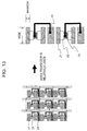
- Fig. 13 shows another structure (refer to Patent Document 2) in which a voltage conversion element 23 and other circuit components are shared between two photoelectric conversion elements 21 and two readout gates 22 and the shared circuit components are arranged in each transistor region 24 adjacent to the photoelectric conversion elements 21.
- the photoelectric conversion elements and the component transistors cannot actually be arranged uniformly. Therefore, the degree of sharing the component transistors is not always proportional to the area occupancy ratio of the photoelectric conversion element. The reason is that the size of a component transistor in each small pixel is large relative to the pixel size and flexibility in shape is not high due to the limits of manufacturing techniques and those of physical properties. It is absolutely essential that the optical centers of pixels be equally spaced two-dimensionally and all of pixels have the same fundamental characteristics.
- the component transistors can be arranged in a space between the photoelectric conversion elements 21.
- the spacing between transistors or that between interconnects used for connection becomes narrower. This leads to poor design flexibility. It is difficult to allocate the photoelectric conversion element 21 to the optical center (pixel center) of each pixel.
- a region for the photoelectric conversion element 21 is separated from the transistor region 24. Accordingly, this structure is efficient in terms of pixel arrangement. A well-balanced arrangement layout can also be provided. However, since the transistor regions 24 and the regions for the photoelectric conversion elements 21 are aligned, even if the transistor region 24 is large, the region for the photoelectric conversion element 21 is widely reduced. Consequently, it is difficult to allocate the photoelectric conversion element 21 to the optical center (pixel center) of each pixel. It is further difficult to ensure the amount of signal charge accumulatable in each photoelectric conversion element 21.
- FIG. 14 In addition to the multi-pixel sharing structures shown in Figs. 12 and 13, another multi-pixel sharing structure in Fig. 14 is available. According to the structure, the photoelectric conversion elements 21 are vertically arranged. In this multi-pixel sharing structure, however, since the number of shared voltage conversion elements 23 is few and the capacity of a diffusion layer increases. Unfortunately, voltage conversion efficiency may decrease. Further, the other multi-pixel sharing structure in Fig. 15 is also available. In the structure, sharing in the vertical direction is combined with that in the horizontal direction. In this multi-pixel sharing structure, it is necessary to read out signals of one row such that the signals are divided into two parts. Disadvantageously, output signals may be different from typical video signals.
- a solid-state imaging device including photoelectric conversion elements arranged in a two-dimensional array and voltage conversion elements for converting charge produced by photoelectric conversion through the photoelectric conversion elements into voltage, wherein each of said voltage conversion elements is arranged between two diagonally adjacent photoelectric conversion elements in the two-dimensional array and is shared between the two photoelectric conversion elements.
- the present invention provides a solid-state imaging apparatus comprising photoelectric conversion elements arranged in a two-dimensional array and voltage conversion elements which convert charge generated by photoelectric conversion through the corresponding photoelectric conversion elements into voltage and an optical system through which incident light gets to said photoelectric conversion elements, wherein each of said voltage conversion elements is arranged between two diagonally adjacent photoelectric conversion elements in the two-dimensional array and is shared between the two photoelectric conversion elements.
- FIGs. 1 to 3C show an example of the schematic structure of a CMOS sensor according to the first embodiment.
- Fig. 1 shows an example of the layout of components.
- Figs. 2A and 2B show an example of the circuit configuration.
- Figs. 3B and 3C show examples of signal readout.
- the CMOS sensor includes photoelectric conversion elements 1 for photoelectric conversion, voltage conversion elements 2 for converting charge produced by photoelectric conversion through the photoelectric conversion element into a voltage signal, transfer gates 3 for controlling the readout of charge from the photoelectric conversion element 1 to the voltage conversion element 2, transistor regions 4 where circuit sets (i.e., sets of circuit components including transistors such as a reset gate and similar components) for processing voltage signals obtained through the corresponding voltage conversion elements are arranged, and interconnects 5 for electrically connecting the voltage conversion elements 2 to the corresponding circuit set in the transistor regions 4.
- the components 1 to 5 are substantially similar to those of a known COM sensor. Accordingly, a detailed description of the components is omitted.
- the CMOS sensor has a structure in which the photoelectric conversion elements 1 are arranged in a two-dimensional array including a plurality of columns and a plurality of rows, each voltage conversion element 2 is arranged between two diagonally adjacent photoelectric conversion elements 1 in the two-dimensional array, and each voltage conversion element 2 is shared between the two photoelectric conversion elements 1 through the transfer gates 3 respectively provided for the corresponding photoelectric conversion elements 1.
- the transfer gates 3 respectively provided for the corresponding photoelectric conversion elements 1.
- one voltage conversion element 2 is shared between the photoelectric conversion element 1 at coordinates (i+1, j) and that at coordinates (i, j+1) and another voltage conversion element 2 is shared between the photoelectric conversion element 1 at coordinates (i+1, j+2) and that at coordinates (i, j+3).
- each transistor region 4 is arranged between the photoelectric conversion elements 1, with no voltage conversion element 2 therebetween.
- Each circuit set distributed in the transistor regions 4 is shared between the two voltage conversion elements 2 electrically connected to the circuit set via the interconnect 5.
- the shared circuit set includes a reset (RST) transistor and a select (SEL) transistor. The circuit components are distributed in the transistor regions 4.
- the above-mentioned CMOS sensor has a structure in which one circuit set distributed in two transistor regions 4 aligned in the column direction in the two-dimensional array is shared between two voltage conversion elements 2 aligned in the same column direction, and each of the voltage conversion elements 2 is shared between two diagonally adjacent photoelectric conversion elements 1 in the two-dimensional array.
- One circuit set, two voltage conversion elements 2, and four photoelectric conversion elements 1 constitute one sharing unity (unit block) 6.
- the CMOS sensor has a multi-pixel sharing structure in which one voltage conversion element 2 is arranged between two diagonally adjacent photoelectric conversion elements 1 such that the photoelectric conversion element 1 is shared therebetween. Consequently, the size of each voltage conversion element 2 in the orthogonal direction is 1/ ⁇ 2 of that in a conventional structure in which each voltage conversion element is shared between photoelectric conversion elements aligned in the column or row direction in a two-dimensional array.
- the voltage conversion elements 2 are arranged in this manner, a part of each transfer gate 3 protruded toward the corresponding photoelectric conversion element 1 is small. Thus, the space between the photoelectric conversion elements 1 can be reduced.
- each interconnect 5, extending to the transistor regions 4 separately arranged in the column direction, has a simple form such that the interconnect 5 hardly interferes with another interconnect 5.
- each photoelectric conversion element 1 depends on only the width of isolation. Since it is difficult to reduce the area of the transistor region 4, area efficiency is increased depending on the arrangement of the voltage conversion elements 2, which are substantially shape-independent. A free space between the diagonally adjacent photoelectric conversion elements 1 is effectively used for the arrangement of the voltage conversion element 2, thus reducing an invalid region in the vicinity of the voltage conversion element 2. Consequently, each space between the photoelectric conversion elements 1 (distance therebetween in the column or row direction in the two-dimensional array) can be reduced. In addition, the sufficient area of a region for the photoelectric conversion element 1 relative to each pixel area can be secured. Furthermore, the photoelectric conversion element 1 is allocated to the optical center of each pixel, so that the optical pixel centers can easily be equally spaced two-dimensionally.
- the area of the region for each photoelectric conversion element 1 can be increased and equally spacing the pixel centers can be easily realized.
- the amount of saturation signal in the photoelectric conversion element 1 increases due to the increase in area of the region for the photoelectric conversion element 1, thus improving dynamic range.
- the amount of signal charge is larger, the relative amount of random noise becomes smaller under high light conditions, thus increasing the S/N ratio. An increase in image quality of an output signal can be expected.
- the circuit components constituting one circuit set are distributed in two transistor regions 4. Accordingly, the well-balanced uniform arrangement of the circuit set can be assigned to the corresponding photoelectric conversion elements 1 in the two-dimensional array. Even if it is difficult to reduce the area of the transistor region 4, therefore, the sufficient area of the region for the photoelectric conversion element 1 can be secured relative to each pixel area.
- the photoelectric conversion element 1 is allocated to the optical center of each pixel, so that the optical pixel centers can easily be equally spaced two-dimensionally.
- one sharing unity 6 includes four photoelectric conversion elements 1, i.e., the case of sharing by four pixels.
- the present invention is not limited to this case. So long as the sharing relationship is established between even-numbered pixels, similar driving can be realized.
- the capacitance of the voltage conversion element 2 increases. Therefore, an output voltage of the voltage conversion element 2 tends to lower relative to the amount of signal charge. This reduces the amplitude of an input signal to be supplied to amplification portion. This may lead to degradation in noise immunity.
- the area of each photoelectric conversion element 1 becomes larger. The rate of increase in area depends on the degree of sharing with respect to shared circuit components. Accordingly, as the sharing degree increases, the increase rate decreases.
- the capacitance of the voltage conversion element 2 can be improved by optimizing the concentration of an impurity, the improvement is limited. Accordingly, the sharing by four pixels described in the first embodiment is the most balanced sharing structure.
- each voltage conversion element 2 is shared between diagonally adjacent photoelectric conversion elements 1.
- red (R) and green (G) alternate in order of R, G, R, G, ... in a row in a two-dimensional array
- green and blue (B) alternate in order of G, B, G, B, ... in the next row.
- G is assigned to each of four photoelectric conversion elements 1 in one sharing unity 6.
- R is assigned to two of the four elements and B is assigned to the other two elements.
- one sharing unity 6 includes two pairs of photoelectric conversion elements 1, each pair having the same spectral sensitivity. The same color is assigned to the photoelectric conversion elements 1 in the odd-numbered rows and the other same color is assigned to those in the even-numbered rows.
- the CMOS sensor supports a driving mode in which charge is simultaneously read out from the photoelectric conversion elements 1 having the same spectral sensitivity among the photoelectric conversion elements 1 constituting one sharing unity 6 and signals based on charge are added through the voltage conversion elements 2 in the sharing unity 6.
- high-speed signal readout from the photoelectric conversion elements 1 can also be performed.
- the voltage conversion elements 2 can perform charge addition of two rows with respect to the same-color photoelectric conversion elements. Consequently, the number of output rows is reduced to 1/2, thus realizing high-speed signal readout.
- the CMOS sensor has a structure in which in each sharing unity, the circuit set is shared between two voltage conversion elements 2 in the column direction in the two-dimensional array, i.e., the two voltage conversion elements 2 are aligned vertically. Therefore, driving signals for simultaneous readout are supplied to the circuit sets arranged in the same row in the two-dimensional array, so that it is easily possible to simultaneously read charge from the photoelectric conversion elements 1 arranged in the same row in the two-dimensional array.
- pixels (photoelectric conversion elements) sharing each voltage conversion element 2 are assigned to different rows in the two-dimensional array. Thus, signals based on charge can be simultaneously read out every row.
- Fig. 4 is a diagram explaining an example of the schematic structure of a CMOS sensor according to the second embodiment.
- a plurality of signal lines 7 to read a voltage signal processed through each circuit set are arranged in each column in a two-dimensional array.
- the voltage signals are simultaneously read out from a plurality of sharing unities 6 arranged in the column direction in the two-dimensional array through the signal lines 7.
- signal outputs of the sharing unities 6 are simultaneously obtained every column, so that time required to obtain one image is reduced depending on the number of outputs. In other words, higher speed driving can be realized.
- FIGs. 5 and 6 are diagrams explaining examples of the schematic structure of a CMOS sensor according to the third embodiment.
- the CMOS sensor includes signal sequence permutation portion for correcting the difference in read-out signal sequence between the odd-numbered row and the even-numbered row in the two-dimensional array, the difference being caused by sharing each voltage conversion element 2 between diagonally adjacent photoelectric conversion elements 1. The reason is as follows.
- each signal line 7 to read a signal is connected to a row circuit 9 through a column selection switch 8 in a two-dimensional array such that a signal is generated from the signal line 7 to the row circuit 9.
- a multi-pixel sharing structure that each voltage conversion element 2 is shared between two diagonally adjacent photoelectric conversion elements 1, outputs of the photoelectric conversion elements 1 in the odd-numbered and even-numbered rows are supplied through different signal lines 7 to the row circuit 9.
- the CMOS sensor according to the third embodiment includes the signal sequence permutation portion.
- signal outputs from the signal lines 7 to the row circuit 9 are controlled by cascade connection of delay circuits 10 as shown in the diagram.
- Time-shifted signals are sequentially input to the column selection switches 8 in the respective columns.
- the signal sequence permutation portion delays an input signal to be supplied to the first stage so that the input signal is timed to data output of the general CMOS sensor.
- one delay circuit 11 may be arranged upstream of the first input stage and a switch 12 to bypass the delay circuit 11 can be further disposed.
- a switch 13 can be arranged so as to select two of control signals supplied to the respective columns from a series of delay circuits 10. The two selected control signals correspond to time-shifted readout signals of one column.
- analog signals supplied to an amplifier 9a at an output terminal of the row circuit 9 are not different from those of a general pixel array.
- the CMOS sensor since the CMOS sensor includes the signal sequence permutation portion, readout between the odd-numbered rows and the even-numbered rows can be switched. Accordingly, readout can be controlled using a timing signal synchronized with a control signal of the transfer gate 3. Thus, a special functional circuit is not needed.
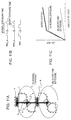
- FIG. 7 is a diagram explaining the amounts of produced charge of respective color components.
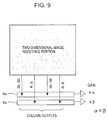
- Figs. 8 and 9 are diagrams explaining examples of the schematic structure of a CMOS sensor according to the fourth embodiment.
- CMOS sensor In the CMOS sensor according to the fourth embodiment, a Bayer-pattern color filter array is arranged such that color filters are assigned to photoelectric conversion elements 1 arranged in a two-dimensional array, respectively (refer to Fig. 3A) .
- the CMOS sensor is constructed such that an amplification factor with respect to an output voltage signal of each odd-numbered column in the two-dimensional array is different from that of each even-numbered column, i.e., signal amplification factors of signal lines to output voltage signals are different from each other. The reason is as follows.
- each voltage conversion element 2 is shared between two diagonally adjacent photoelectric conversion elements 1
- signal lines are divided into output lines (Gr/Gb output lines) shared between Gr (G signals of columns where R pixels are arranged) and Gb (G signals of columns where B pixels are arranged) and output lines (B/R output lines) shared between B and R.
- the B signal has such properties that the amount of produced charge is small and there is a loss due to the absorption of photons on the surface p+
- the R signal has such properties that most photons are not absorbed in the depth, where pn junction can be formed, of the photoelectric conversion element 1.
- the G signal has the minimum loss and a G signal output has a tendency to become larger. Therefore, if the gain (amplification factor) of each Gr/Gb output line is different from that of each B/R output line, the difference in spectral characteristic between RGB in chip output can be reduced.
- each Gr/Gb output line is reduced and the gain of each B/R output line is increased. Since a known technique can be used for setting the gains, a description about setting is omitted.
- the CMOS sensor has a structure in which a signal output from each column is converted into a digital signal by AD conversion portion (e.g., an AD converter) provided for each column and digital signals generated from a plurality of columns are sequentially supplied to one signal output portion (e.g., a column circuit or an amplifier), the respective digital signals are subjected to gain adjustment such that the difference in spectral characteristic between RGB is reduced. Accordingly, the signal output portion can perform the digital signals uniformly, i.e., using the same process parameters.
- AD conversion portion e.g., an AD converter
- outputs of the odd-numbered columns and those of the even-numbered columns in the two-dimensional array are connected to two different row circuits 9b and 9c, respectively.
- the signal amplification factor of the signal line in each odd-numbered column is not different from that in each even-numbered column, so long as the gains of the two row circuits 9b and 9c are different from each other, the difference in spectral characteristic between RBG in chip output can be reduced.
- the gains of the row circuits 9b and 9c are different from each other, the gains can be set using a known technique. A description of the gain setting is omitted.
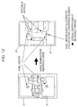
- FIG. 10A and 10B explain an example of the schematic structure of a CMOS sensor according to the fifth embodiment.
- a Bayer-pattern color filter array is arranged such that color filters are assigned to photoelectric conversion elements 1 disposed in a two-dimensional array, respectively.
- the difference between output signals caused by difference in pixel layout is corrected. The reason is as follows.
- each voltage conversion element is shared between a plurality of photoelectric conversion elements. Since the shapes of the photoelectric conversion elements are symmetric, the amounts of produced signal may be different from each other due to a pattern misalignment in a manufacturing process or a variation in light incidence angle upon receiving light.
- each voltage conversion element 2 is shared between two diagonally adjacent photoelectric conversion elements 1
- each Gr pixel and each Gb pixel is connected to the same voltage conversion element 2 and the Gr and Gb pixels belong to different rows. Therefore, there are the same combinations of components other than the pixel, i.e., the color and subsequent-stage connected circuits. Thus, the difference in amount of produced signal caused by difference in pixel shape can be easily corrected.
- the output signal difference caused by the difference in pixel layout (arrangement position and the shape of the photoelectric conversion element) between two diagonally adjacent photoelectric conversion elements 1 is corrected using correction coefficients shown in Fig. 10B.
- the correction is applied to output signals from the B and R pixels.
- the output signal difference caused by the difference in pixel layout is corrected.
- signal outputs with small output variations can be realized.
- a correction error can be reduced and correction coefficients can be easily calculated.
- the above-mentioned correcting process can be easily applied to digital signals subjected to AD conversion.
- the correcting process for signal output can be performed using a known technique in a manner similar to the gain adjustment described in the fourth embodiment. A description of the correcting process is omitted.
- FIGS. 11A to 11C are diagrams explaining an example of the schematic structure of a CMOS sensor according to the sixth embodiment.
- the CMOS sensor according to the sixth embodiment supports a driving mode for signal addition based on charge in voltage conversion elements 2 constituting each sharing unity 6.
- the CMOS sensor is constructed such that in addition to the use of a charge addition function in the driving mode, photoelectric conversion times of photoelectric conversion elements 1, from which charge is simultaneously read out for the signal addition based on charge, are different from each other. The reason is as follows.
- pixels sharing the voltage conversion elements 2 via an interconnect 5 include pixels having the same spectral characteristic, i.e., the pixels to which the same-color filters are assigned. Accordingly, the charge addition function can be used.
- photoelectric conversion time of at least one photoelectric conversion element 1 connected to one voltage conversion element 2 is different from that of at least one photoelectric conversion element 1 connected to the other voltage conversion element 2.
- the sensitivity to low bright light is higher than that to high bright light, i.e., a wide dynamic range can be realized.
- the difference in photoelectric conversion time can be made by controlling readout pulses as shown in Fig. 11B. Under condition that the difference in photoelectric conversion time is provided, for example, when high bright light is incident, a pixel with normal accumulation time is saturated but a pixel with delayed accumulation start time is not saturated, thus obtaining the characteristics depending on light intensity. When the amounts of signal charge are added in the shared voltage conversion elements 2, therefore, an added signal output represents sensitivity characteristic as shown in Fig. 11C.
- the above-mentioned solid-state imaging device has a multi-pixel sharing structure in which one voltage conversion element is arranged between two diagonally adjacent photoelectric conversion elements such that the voltage conversion element is shared therebetween. Consequently, the size of each voltage conversion element in the orthogonal direction is 1/ ⁇ 2 of that in a conventional structure in which each voltage conversion element is shared between photoelectric conversion elements aligned in the column or row direction in a two-dimensional array. In other words, a free space between the diagonally adjacent photoelectric conversion elements is effectively used for the arrangement of the voltage conversion element, thus reducing an invalid region in the vicinity of the voltage conversion element. Consequently, each space between the photoelectric conversion elements (distance therebetween in the column or row direction in the two-dimensional array) can be reduced.
- the sufficient area of a region for the photoelectric conversion element relative to each pixel area can be secured.
- the photoelectric conversion element is allocated to the optical center of each pixel, so that the optical pixel centers can easily be equally spaced two-dimensionally.
- pixels (photoelectric conversion elements) sharing each voltage conversion element are allocated to different rows in the two-dimensional array.
- signals can be simultaneously read out every row.
- color filters are formed in respective pixels according to a Bayer pattern, the same color is assigned to the photoelectric conversion elements in the odd-numbered rows and the same color is assigned to those in the even-numbered rows in each sharing unity.
- the voltage conversion elements can perform charge addition of two rows with respect to the same-color photoelectric conversion elements. Consequently, high-speed signal readout from the photoelectric conversion elements can also be performed.
- the formation of an invalid region in the vicinity of each shared voltage conversion element can be suppressed.
- the area of the region for each photoelectric conversion element can be increased and equally spacing the pixel centers can be easily realized. Therefore, the amount of saturation signal in the photoelectric conversion element increases due to the increase in area of the region for the photoelectric conversion element, thus improving dynamic range. As the amount of signal charge is larger, the relative amount of random noise becomes smaller under high light conditions, thus increasing the S/N ratio. An increase in image quality of an output signal can be expected.
- high-speed signal readout can be performed depending on a driving mode.
- the present invention is also applied to an imaging apparatus, for instance, a camera or a camera module.
Landscapes
- Engineering & Computer Science (AREA)
- Multimedia (AREA)
- Signal Processing (AREA)
- Solid State Image Pick-Up Elements (AREA)
- Transforming Light Signals Into Electric Signals (AREA)
Applications Claiming Priority (1)
| Application Number | Priority Date | Filing Date | Title |
|---|---|---|---|
| JP2004234061A JP4492250B2 (ja) | 2004-08-11 | 2004-08-11 | 固体撮像素子 |
Publications (3)
| Publication Number | Publication Date |
|---|---|
| EP1628468A2 true EP1628468A2 (fr) | 2006-02-22 |
| EP1628468A3 EP1628468A3 (fr) | 2007-11-07 |
| EP1628468B1 EP1628468B1 (fr) | 2012-03-28 |
Family
ID=35464178
Family Applications (1)
| Application Number | Title | Priority Date | Filing Date |
|---|---|---|---|
| EP05017430A Expired - Lifetime EP1628468B1 (fr) | 2004-08-11 | 2005-08-10 | Dispositif de prise d'images à l'état solide et appareil de prise d'images |
Country Status (6)
| Country | Link |
|---|---|
| US (1) | US7812878B2 (fr) |
| EP (1) | EP1628468B1 (fr) |
| JP (1) | JP4492250B2 (fr) |
| KR (1) | KR101104617B1 (fr) |
| CN (1) | CN100424883C (fr) |
| TW (1) | TWI282689B (fr) |
Cited By (5)
| Publication number | Priority date | Publication date | Assignee | Title |
|---|---|---|---|---|
| EP2151828A1 (fr) * | 2008-08-04 | 2010-02-10 | STMicroelectronics (Research & Development) Limited | Circuit de mémoire à accès aléatoire |
| EP2309541A3 (fr) * | 2009-10-06 | 2013-04-17 | Canon Kabushiki Kaisha | Capteur d'image à l'état solide et appareil de détection d'image |
| EP2512126A4 (fr) * | 2010-06-01 | 2014-01-01 | Boly Media Comm Shenzhen Co | Dispositif photoréceptif multispectral et son procédé d'échantillonnage |
| EP2351356A4 (fr) * | 2008-10-22 | 2014-09-10 | Canon Kk | Capteur d image et appareil de détection d image |
| US9160955B2 (en) | 2007-11-30 | 2015-10-13 | Sony Corporation | Solid-state imaging device and camera |
Families Citing this family (61)
| Publication number | Priority date | Publication date | Assignee | Title |
|---|---|---|---|---|
| JP2006042267A (ja) * | 2004-07-30 | 2006-02-09 | Canon Inc | 画像処理方法、画像処理装置、およびプログラム |
| KR100598015B1 (ko) * | 2005-02-07 | 2006-07-06 | 삼성전자주식회사 | 공유 구조 상보성 금속 산화막 반도체 액티브 픽셀 센서어레이의 레이 아웃 |
| JP4695979B2 (ja) * | 2005-12-26 | 2011-06-08 | パナソニック株式会社 | 固体撮像装置 |
| JP4915127B2 (ja) * | 2006-04-10 | 2012-04-11 | ソニー株式会社 | 固体撮像装置 |
| JP2008072098A (ja) * | 2006-08-17 | 2008-03-27 | Sony Corp | 半導体イメージセンサ |
| US7916195B2 (en) * | 2006-10-13 | 2011-03-29 | Sony Corporation | Solid-state imaging device, imaging apparatus and camera |
| JP4341664B2 (ja) * | 2006-10-13 | 2009-10-07 | ソニー株式会社 | 固体撮像装置および撮像装置 |
| KR100790583B1 (ko) | 2006-10-16 | 2008-01-02 | (주) 픽셀플러스 | 씨모스 이미지 센서 공유 픽셀 |
| KR100790582B1 (ko) | 2006-10-16 | 2008-01-02 | (주) 픽셀플러스 | 씨모스 이미지 센서 픽셀 |
| KR100976886B1 (ko) | 2006-12-22 | 2010-08-18 | 크로스텍 캐피탈, 엘엘씨 | 부동 베이스 판독 개념을 갖는 cmos 이미지 센서 |
| US7839439B2 (en) | 2007-01-12 | 2010-11-23 | Sony Corporation | Solid-state imaging device and imaging device |
| JP5584982B2 (ja) * | 2009-02-09 | 2014-09-10 | ソニー株式会社 | 固体撮像素子およびカメラシステム |
| JP4292426B2 (ja) * | 2007-05-15 | 2009-07-08 | ソニー株式会社 | 撮像装置および撮像データ補正方法 |
| JP5076635B2 (ja) | 2007-05-17 | 2012-11-21 | ソニー株式会社 | イメージセンサ |
| JP2009010862A (ja) * | 2007-06-29 | 2009-01-15 | Canon Inc | 撮像装置の駆動方法 |
| US7924333B2 (en) | 2007-08-17 | 2011-04-12 | Aptina Imaging Corporation | Method and apparatus providing shared pixel straight gate architecture |
| JP5187550B2 (ja) * | 2007-08-21 | 2013-04-24 | ソニー株式会社 | 撮像装置 |
| US7964929B2 (en) | 2007-08-23 | 2011-06-21 | Aptina Imaging Corporation | Method and apparatus providing imager pixels with shared pixel components |
| US7989749B2 (en) | 2007-10-05 | 2011-08-02 | Aptina Imaging Corporation | Method and apparatus providing shared pixel architecture |
| KR100858033B1 (ko) * | 2007-10-15 | 2008-09-10 | (주)실리콘화일 | 4t-4s 스텝 & 리피트 단위픽셀 및 상기 단위픽셀을구비하는 이미지센서 |
| JP5045380B2 (ja) * | 2007-11-13 | 2012-10-10 | ソニー株式会社 | 撮像装置および撮像データ補正方法並びにプログラム |
| US8077236B2 (en) | 2008-03-20 | 2011-12-13 | Aptina Imaging Corporation | Method and apparatus providing reduced metal routing in imagers |
| US7667169B2 (en) * | 2008-05-22 | 2010-02-23 | Omnivision Technologies, Inc. | Image sensor with simultaneous auto-focus and image preview |
| JP5181840B2 (ja) * | 2008-05-30 | 2013-04-10 | ソニー株式会社 | 固体撮像装置、固体撮像装置の駆動方法、及び電子機器 |
| US8035716B2 (en) * | 2008-06-13 | 2011-10-11 | Omnivision Technologies, Inc. | Wide aperture image sensor pixel |
| JP5292939B2 (ja) * | 2008-06-20 | 2013-09-18 | ソニー株式会社 | 画像処理装置および方法、製造装置 |
| JP5241454B2 (ja) * | 2008-12-01 | 2013-07-17 | キヤノン株式会社 | 固体撮像装置及びそれを用いた撮像システム |
| GB2466213B (en) * | 2008-12-12 | 2013-03-06 | Cmosis Nv | Pixel array with shared readout circuitry |
| JP5109962B2 (ja) * | 2008-12-22 | 2012-12-26 | ソニー株式会社 | 固体撮像装置および電子機器 |
| JP4760915B2 (ja) | 2009-01-08 | 2011-08-31 | ソニー株式会社 | 固体撮像素子 |
| JP5029624B2 (ja) * | 2009-01-15 | 2012-09-19 | ソニー株式会社 | 固体撮像装置及び電子機器 |
| US8547458B2 (en) | 2009-02-04 | 2013-10-01 | Rosnes Corporation | Solid-state image pickup device |
| US8576312B2 (en) * | 2009-02-04 | 2013-11-05 | Rosnes Corporation | Solid-state image pickup device with particular pixel arrangement |
| JP2010278303A (ja) * | 2009-05-29 | 2010-12-09 | Toshiba Corp | 固体撮像装置 |
| JP2010282992A (ja) | 2009-06-02 | 2010-12-16 | Sony Corp | 固体撮像装置、および、その製造方法、電子機器 |
| JP5375359B2 (ja) | 2009-06-22 | 2013-12-25 | ソニー株式会社 | 撮像素子、電荷読み出し方法、撮像装置 |
| JP5476832B2 (ja) | 2009-07-23 | 2014-04-23 | ソニー株式会社 | 固体撮像装置及びカメラ |
| JP5552768B2 (ja) | 2009-07-27 | 2014-07-16 | ソニー株式会社 | 固体撮像装置とその製造方法、及び電子機器 |
| JP2011035154A (ja) | 2009-07-31 | 2011-02-17 | Sony Corp | 固体撮像装置、および、その製造方法、電子機器 |
| JP5471174B2 (ja) | 2009-08-28 | 2014-04-16 | ソニー株式会社 | 固体撮像装置とその製造方法、及び電子機器 |
| JP5564874B2 (ja) | 2009-09-25 | 2014-08-06 | ソニー株式会社 | 固体撮像装置、及び電子機器 |
| JP2011082253A (ja) | 2009-10-05 | 2011-04-21 | Sony Corp | 固体撮像装置、および、その製造方法、電子機器 |
| JP5564909B2 (ja) | 2009-11-30 | 2014-08-06 | ソニー株式会社 | 固体撮像装置とその製造方法、及び電子機器 |
| JP5475482B2 (ja) * | 2010-01-26 | 2014-04-16 | キヤノン株式会社 | 撮像素子及び撮像装置 |
| JP5537172B2 (ja) * | 2010-01-28 | 2014-07-02 | ソニー株式会社 | 固体撮像装置及び電子機器 |
| DE112011100842T5 (de) | 2010-03-08 | 2013-01-17 | Semiconductor Energy Laboratory Co., Ltd. | Halbleiterbauelement und Verfahren zu dessen Herstellung |
| JP5644177B2 (ja) | 2010-05-07 | 2014-12-24 | ソニー株式会社 | 固体撮像装置、および、その製造方法、電子機器 |
| JP2012059865A (ja) * | 2010-09-08 | 2012-03-22 | Sony Corp | 撮像素子および撮像装置 |
| CN102404515A (zh) * | 2010-09-13 | 2012-04-04 | 联咏科技股份有限公司 | 影像感测装置 |
| US8456557B2 (en) * | 2011-01-31 | 2013-06-04 | SK Hynix Inc. | Dynamic range extension for CMOS image sensors for mobile applications |
| US8749665B2 (en) * | 2011-01-31 | 2014-06-10 | SK Hynix Inc. | Dynamic range extension for CMOS image sensors for mobile applications |
| WO2013008597A1 (fr) | 2011-07-13 | 2013-01-17 | 富士フイルム株式会社 | Appareil de prise d'image, élément de prise d'image et procédé de correction de différence de sensibilité |
| JP5945463B2 (ja) * | 2012-06-28 | 2016-07-05 | オリンパス株式会社 | 固体撮像装置 |
| WO2013145888A1 (fr) * | 2012-03-28 | 2013-10-03 | 富士フイルム株式会社 | Élément de capture d'image à semi-conducteurs, dispositif de capture d'image et procédé de commande d'élément de capture d'image à semi-conducteurs |
| EP2838255A4 (fr) * | 2012-04-09 | 2015-12-09 | Olympus Corp | Dispositif de prise de vue à semi-conducteur |
| JP5764783B2 (ja) * | 2012-04-19 | 2015-08-19 | 国立大学法人東北大学 | 固体撮像装置 |
| FR3030884B1 (fr) * | 2014-12-19 | 2016-12-30 | Stmicroelectronics (Grenoble 2) Sas | Structure de pixel a multiples photosites |
| US9843756B2 (en) | 2015-05-27 | 2017-12-12 | Samsung Electronics Co., Ltd. | Imaging devices, arrays of pixels receiving photocharges in bulk of select transistor, and methods |
| EP3516691B1 (fr) | 2016-10-14 | 2021-09-22 | Huawei Technologies Co., Ltd. | Capteur d'image cmos |
| WO2018207345A1 (fr) * | 2017-05-12 | 2018-11-15 | オリンパス株式会社 | Dispositif de capture d'image à semi-conducteurs |
| JP6967173B1 (ja) | 2021-07-19 | 2021-11-17 | テックポイント インクTechpoint, Inc. | 撮像素子及び撮像装置 |
Family Cites Families (25)
| Publication number | Priority date | Publication date | Assignee | Title |
|---|---|---|---|---|
| US3971065A (en) * | 1975-03-05 | 1976-07-20 | Eastman Kodak Company | Color imaging array |
| JPS58215877A (ja) * | 1982-06-09 | 1983-12-15 | Canon Inc | 撮像装置 |
| JPS6170872A (ja) * | 1984-09-14 | 1986-04-11 | Hitachi Ltd | 固体撮像装置 |
| JPH0638486B2 (ja) * | 1984-12-28 | 1994-05-18 | 株式会社東芝 | 電荷蓄積形半導体装置 |
| JPH0319582A (ja) * | 1989-06-16 | 1991-01-28 | Nec Corp | 固体撮像装置とその駆動方法 |
| JPH04286460A (ja) * | 1991-03-15 | 1992-10-12 | Canon Inc | イメージセンサ |
| US6107655A (en) * | 1997-08-15 | 2000-08-22 | Eastman Kodak Company | Active pixel image sensor with shared amplifier read-out |
| US6956605B1 (en) * | 1998-08-05 | 2005-10-18 | Canon Kabushiki Kaisha | Image pickup apparatus |
| JP3854729B2 (ja) * | 1998-09-02 | 2006-12-06 | キヤノン株式会社 | 撮像装置およびそれを用いた撮像システム |
| JP2000162320A (ja) | 1998-09-22 | 2000-06-16 | Toshiba Corp | 平面検出器及びこれを用いたx線診断装置 |
| US6654057B1 (en) * | 1999-06-17 | 2003-11-25 | Micron Technology, Inc. | Active pixel sensor with a diagonal active area |
| JP2001264014A (ja) * | 2000-03-21 | 2001-09-26 | Fuji Xerox Co Ltd | 光センサおよび三次元形状計測装置 |
| JP4721380B2 (ja) * | 2000-04-14 | 2011-07-13 | キヤノン株式会社 | 固体撮像装置および撮像システム |
| JP2002199284A (ja) * | 2000-12-25 | 2002-07-12 | Canon Inc | 撮像素子 |
| JP2003101881A (ja) * | 2001-09-20 | 2003-04-04 | Sony Corp | 固体撮像装置および固体撮像装置の駆動方法 |
| JP2003189316A (ja) * | 2001-12-19 | 2003-07-04 | Minolta Co Ltd | 撮像センサ |
| US6907632B2 (en) * | 2002-05-28 | 2005-06-21 | Ferno-Washington, Inc. | Tactical stretcher |
| JP2004128193A (ja) * | 2002-10-02 | 2004-04-22 | Iwate Toshiba Electronics Co Ltd | Cmosイメージセンサ |
| JP3751931B2 (ja) * | 2002-11-05 | 2006-03-08 | ローム株式会社 | エリアイメージセンサ |
| JP4601897B2 (ja) * | 2002-11-13 | 2010-12-22 | ソニー株式会社 | 固体撮像装置及びその駆動方法 |
| JP3988189B2 (ja) * | 2002-11-20 | 2007-10-10 | ソニー株式会社 | 固体撮像装置 |
| US7542085B2 (en) * | 2003-11-26 | 2009-06-02 | Aptina Imaging Corporation | Image sensor with a capacitive storage node linked to transfer gate |
| US7250665B1 (en) * | 2004-12-30 | 2007-07-31 | Ess Technology, Inc. | Method and apparatus for removing electrons from CMOS sensor photodetectors |
| JP4695979B2 (ja) * | 2005-12-26 | 2011-06-08 | パナソニック株式会社 | 固体撮像装置 |
| US7839439B2 (en) * | 2007-01-12 | 2010-11-23 | Sony Corporation | Solid-state imaging device and imaging device |
-
2004
- 2004-08-11 JP JP2004234061A patent/JP4492250B2/ja not_active Expired - Lifetime
-
2005
- 2005-08-03 TW TW094126432A patent/TWI282689B/zh not_active IP Right Cessation
- 2005-08-09 CN CNB2005100897588A patent/CN100424883C/zh not_active Expired - Fee Related
- 2005-08-10 KR KR1020050073166A patent/KR101104617B1/ko not_active Expired - Fee Related
- 2005-08-10 US US11/200,687 patent/US7812878B2/en active Active
- 2005-08-10 EP EP05017430A patent/EP1628468B1/fr not_active Expired - Lifetime
Non-Patent Citations (1)
| Title |
|---|
| None |
Cited By (13)
| Publication number | Priority date | Publication date | Assignee | Title |
|---|---|---|---|---|
| EP3151280A1 (fr) * | 2007-11-30 | 2017-04-05 | Sony Corporation | Dispositif et caméra d'imagerie transistorisés |
| US9912892B2 (en) | 2007-11-30 | 2018-03-06 | Sony Corporation | Solid-state imaging device and camera |
| US9899438B2 (en) | 2007-11-30 | 2018-02-20 | Sony Corporation | Solid-state imaging device and camera |
| EP2246887B1 (fr) * | 2007-11-30 | 2017-08-30 | Sony Corporation | Dispositif d'imagerie à l'état solide et caméra |
| US9160955B2 (en) | 2007-11-30 | 2015-10-13 | Sony Corporation | Solid-state imaging device and camera |
| US8456885B2 (en) | 2008-08-04 | 2013-06-04 | STMicroelectronics (R&D) Ltd. | Random access memory circuit |
| EP2151828A1 (fr) * | 2008-08-04 | 2010-02-10 | STMicroelectronics (Research & Development) Limited | Circuit de mémoire à accès aléatoire |
| EP2351356A4 (fr) * | 2008-10-22 | 2014-09-10 | Canon Kk | Capteur d image et appareil de détection d image |
| US9294744B2 (en) | 2008-10-22 | 2016-03-22 | Canon Kabushiki Kaisha | Image sensor and image sensing apparatus with plural vertical output lines |
| US8913168B2 (en) | 2009-10-06 | 2014-12-16 | Canon Kabushiki Kaisha | Solid-state image sensor and image sensing apparatus |
| US8659692B2 (en) | 2009-10-06 | 2014-02-25 | Canon Kabushiki Kaisha | Solid-state image sensor and image sensing apparatus |
| EP2309541A3 (fr) * | 2009-10-06 | 2013-04-17 | Canon Kabushiki Kaisha | Capteur d'image à l'état solide et appareil de détection d'image |
| EP2512126A4 (fr) * | 2010-06-01 | 2014-01-01 | Boly Media Comm Shenzhen Co | Dispositif photoréceptif multispectral et son procédé d'échantillonnage |
Also Published As
| Publication number | Publication date |
|---|---|
| KR20060050362A (ko) | 2006-05-19 |
| EP1628468B1 (fr) | 2012-03-28 |
| US7812878B2 (en) | 2010-10-12 |
| KR101104617B1 (ko) | 2012-01-12 |
| TW200618613A (en) | 2006-06-01 |
| EP1628468A3 (fr) | 2007-11-07 |
| US20060038904A1 (en) | 2006-02-23 |
| JP2006054276A (ja) | 2006-02-23 |
| TWI282689B (en) | 2007-06-11 |
| JP4492250B2 (ja) | 2010-06-30 |
| CN100424883C (zh) | 2008-10-08 |
| CN1734779A (zh) | 2006-02-15 |
Similar Documents
| Publication | Publication Date | Title |
|---|---|---|
| US7812878B2 (en) | Solid-state imaging device and imaging apparatus | |
| JP5089017B2 (ja) | 固体撮像装置及び固体撮像システム | |
| US7859581B2 (en) | Image sensor with charge binning and dual channel readout | |
| US9832405B2 (en) | Solid-state imaging device with a plurality of photoelectric converters | |
| KR101497715B1 (ko) | 고체 촬상 장치 및 카메라 | |
| US20080088724A1 (en) | Solid-state imaging device, imaging apparatus and camera | |
| US9257465B2 (en) | Solid-state imaging device and electronic apparatus with increased length of amplifying portion | |
| JP2006073733A (ja) | 固体撮像装置及び固体撮像システム | |
| JP5526342B2 (ja) | 固体撮像装置 | |
| US20250193541A1 (en) | Hybrid imaging sensor with high sampling point distribution | |
| CN101071820A (zh) | 固体成像装置 | |
| CN207251823U (zh) | 成像设备和成像系统 | |
| KR20140039953A (ko) | 고체 촬상 장치, 촬상 방법 및 카메라 모듈 | |
| JP2008263072A (ja) | 固体撮像装置 | |
| JP5619093B2 (ja) | 固体撮像装置及び固体撮像システム | |
| US20250255029A1 (en) | Image sensing device | |
| JP2006254144A (ja) | 固体撮像素子 |
Legal Events
| Date | Code | Title | Description |
|---|---|---|---|
| PUAI | Public reference made under article 153(3) epc to a published international application that has entered the european phase |
Free format text: ORIGINAL CODE: 0009012 |
|
| AK | Designated contracting states |
Kind code of ref document: A2 Designated state(s): AT BE BG CH CY CZ DE DK EE ES FI FR GB GR HU IE IS IT LI LT LU LV MC NL PL PT RO SE SI SK TR |
|
| AX | Request for extension of the european patent |
Extension state: AL BA HR MK YU |
|
| PUAL | Search report despatched |
Free format text: ORIGINAL CODE: 0009013 |
|
| AK | Designated contracting states |
Kind code of ref document: A3 Designated state(s): AT BE BG CH CY CZ DE DK EE ES FI FR GB GR HU IE IS IT LI LT LU LV MC NL PL PT RO SE SI SK TR |
|
| AX | Request for extension of the european patent |
Extension state: AL BA HR MK YU |
|
| 17P | Request for examination filed |
Effective date: 20080410 |
|
| 17Q | First examination report despatched |
Effective date: 20080516 |
|
| AKX | Designation fees paid |
Designated state(s): DE FR GB |
|
| REG | Reference to a national code |
Ref country code: DE Ref legal event code: R079 Ref document number: 602005033340 Country of ref document: DE Free format text: PREVIOUS MAIN CLASS: H04N0003150000 Ipc: H01L0027146000 |
|
| GRAP | Despatch of communication of intention to grant a patent |
Free format text: ORIGINAL CODE: EPIDOSNIGR1 |
|
| RIC1 | Information provided on ipc code assigned before grant |
Ipc: H04N 5/3745 20110101ALI20110816BHEP Ipc: H01L 27/146 20060101AFI20110816BHEP |
|
| RIN1 | Information on inventor provided before grant (corrected) |
Inventor name: KUDOH, YOSHIHARU |
|
| GRAS | Grant fee paid |
Free format text: ORIGINAL CODE: EPIDOSNIGR3 |
|
| GRAA | (expected) grant |
Free format text: ORIGINAL CODE: 0009210 |
|
| RIN1 | Information on inventor provided before grant (corrected) |
Inventor name: KUDOH, YOSHIHARU |
|
| RAP1 | Party data changed (applicant data changed or rights of an application transferred) |
Owner name: SONY CORPORATION |
|
| AK | Designated contracting states |
Kind code of ref document: B1 Designated state(s): DE FR GB |
|
| REG | Reference to a national code |
Ref country code: GB Ref legal event code: FG4D |
|
| REG | Reference to a national code |
Ref country code: DE Ref legal event code: R082 Ref document number: 602005033340 Country of ref document: DE Representative=s name: MUELLER - HOFFMANN & PARTNER PATENTANWAELTE, DE Ref country code: DE Ref legal event code: R082 Ref document number: 602005033340 Country of ref document: DE Representative=s name: MUELLER HOFFMANN & PARTNER PATENTANWAELTE MBB, DE |
|
| REG | Reference to a national code |
Ref country code: DE Ref legal event code: R096 Ref document number: 602005033340 Country of ref document: DE Effective date: 20120524 |
|
| PLBE | No opposition filed within time limit |
Free format text: ORIGINAL CODE: 0009261 |
|
| STAA | Information on the status of an ep patent application or granted ep patent |
Free format text: STATUS: NO OPPOSITION FILED WITHIN TIME LIMIT |
|
| 26N | No opposition filed |
Effective date: 20130103 |
|
| REG | Reference to a national code |
Ref country code: DE Ref legal event code: R097 Ref document number: 602005033340 Country of ref document: DE Effective date: 20130103 |
|
| PGFP | Annual fee paid to national office [announced via postgrant information from national office to epo] |
Ref country code: FR Payment date: 20140821 Year of fee payment: 10 Ref country code: GB Payment date: 20140820 Year of fee payment: 10 |
|
| REG | Reference to a national code |
Ref country code: DE Ref legal event code: R084 Ref document number: 602005033340 Country of ref document: DE |
|
| REG | Reference to a national code |
Ref country code: DE Ref legal event code: R084 Ref document number: 602005033340 Country of ref document: DE Effective date: 20150410 |
|
| GBPC | Gb: european patent ceased through non-payment of renewal fee |
Effective date: 20150810 |
|
| REG | Reference to a national code |
Ref country code: FR Ref legal event code: ST Effective date: 20160429 |
|
| PG25 | Lapsed in a contracting state [announced via postgrant information from national office to epo] |
Ref country code: GB Free format text: LAPSE BECAUSE OF NON-PAYMENT OF DUE FEES Effective date: 20150810 |
|
| PG25 | Lapsed in a contracting state [announced via postgrant information from national office to epo] |
Ref country code: FR Free format text: LAPSE BECAUSE OF NON-PAYMENT OF DUE FEES Effective date: 20150831 |
|
| PGFP | Annual fee paid to national office [announced via postgrant information from national office to epo] |
Ref country code: DE Payment date: 20190822 Year of fee payment: 15 |
|
| REG | Reference to a national code |
Ref country code: DE Ref legal event code: R119 Ref document number: 602005033340 Country of ref document: DE |
|
| PG25 | Lapsed in a contracting state [announced via postgrant information from national office to epo] |
Ref country code: DE Free format text: LAPSE BECAUSE OF NON-PAYMENT OF DUE FEES Effective date: 20210302 |