EP1629539B1 - Verfahren zur herstellung einer thermoelektrischen vorrichtung - Google Patents
Verfahren zur herstellung einer thermoelektrischen vorrichtung Download PDFInfo
- Publication number
- EP1629539B1 EP1629539B1 EP04733420A EP04733420A EP1629539B1 EP 1629539 B1 EP1629539 B1 EP 1629539B1 EP 04733420 A EP04733420 A EP 04733420A EP 04733420 A EP04733420 A EP 04733420A EP 1629539 B1 EP1629539 B1 EP 1629539B1
- Authority
- EP
- European Patent Office
- Prior art keywords
- substrate
- foil
- strip
- groups
- rigid
- Prior art date
- Legal status (The legal status is an assumption and is not a legal conclusion. Google has not performed a legal analysis and makes no representation as to the accuracy of the status listed.)
- Expired - Lifetime
Links
- 238000004519 manufacturing process Methods 0.000 title claims abstract description 13
- 239000000758 substrate Substances 0.000 claims abstract description 62
- 239000011888 foil Substances 0.000 claims abstract description 47
- 238000000034 method Methods 0.000 claims abstract description 34
- 239000004065 semiconductor Substances 0.000 claims abstract description 22
- 239000000463 material Substances 0.000 claims abstract description 19
- 239000010410 layer Substances 0.000 claims description 29
- 239000012790 adhesive layer Substances 0.000 claims description 15
- 238000000227 grinding Methods 0.000 claims description 8
- 239000004020 conductor Substances 0.000 claims description 6
- 229910021421 monocrystalline silicon Inorganic materials 0.000 claims description 5
- 239000004642 Polyimide Substances 0.000 claims description 4
- 229920001721 polyimide Polymers 0.000 claims description 4
- FIHBHSQYSYVZQE-UHFFFAOYSA-N 6-prop-2-enoyloxyhexyl prop-2-enoate Chemical compound C=CC(=O)OCCCCCCOC(=O)C=C FIHBHSQYSYVZQE-UHFFFAOYSA-N 0.000 claims description 3
- 239000000853 adhesive Substances 0.000 claims description 3
- 230000001070 adhesive effect Effects 0.000 claims description 3
- 238000002513 implantation Methods 0.000 claims description 3
- 229910021420 polycrystalline silicon Inorganic materials 0.000 claims description 3
- 125000004430 oxygen atom Chemical group O* 0.000 claims 1
- 230000015572 biosynthetic process Effects 0.000 abstract description 3
- 238000005498 polishing Methods 0.000 abstract 1
- 229910052782 aluminium Inorganic materials 0.000 description 9
- XAGFODPZIPBFFR-UHFFFAOYSA-N aluminium Chemical compound [Al] XAGFODPZIPBFFR-UHFFFAOYSA-N 0.000 description 9
- 230000004048 modification Effects 0.000 description 9
- 238000012986 modification Methods 0.000 description 9
- XUIMIQQOPSSXEZ-UHFFFAOYSA-N Silicon Chemical compound [Si] XUIMIQQOPSSXEZ-UHFFFAOYSA-N 0.000 description 6
- 239000011521 glass Substances 0.000 description 6
- VYPSYNLAJGMNEJ-UHFFFAOYSA-N silicon dioxide Inorganic materials O=[Si]=O VYPSYNLAJGMNEJ-UHFFFAOYSA-N 0.000 description 6
- 229920003002 synthetic resin Polymers 0.000 description 6
- 239000000057 synthetic resin Substances 0.000 description 6
- 238000005530 etching Methods 0.000 description 5
- 229910052710 silicon Inorganic materials 0.000 description 5
- 239000010703 silicon Substances 0.000 description 5
- RYGMFSIKBFXOCR-UHFFFAOYSA-N Copper Chemical compound [Cu] RYGMFSIKBFXOCR-UHFFFAOYSA-N 0.000 description 4
- 238000005229 chemical vapour deposition Methods 0.000 description 4
- 239000011889 copper foil Substances 0.000 description 3
- -1 oxygen ions Chemical class 0.000 description 3
- 238000000206 photolithography Methods 0.000 description 3
- 235000012239 silicon dioxide Nutrition 0.000 description 3
- 239000004593 Epoxy Substances 0.000 description 2
- 239000003990 capacitor Substances 0.000 description 2
- 229910052760 oxygen Inorganic materials 0.000 description 2
- 239000001301 oxygen Substances 0.000 description 2
- 238000001020 plasma etching Methods 0.000 description 2
- 239000000377 silicon dioxide Substances 0.000 description 2
- 239000000126 substance Substances 0.000 description 2
- 238000003631 wet chemical etching Methods 0.000 description 2
- 241001050985 Disco Species 0.000 description 1
- 229910052581 Si3N4 Inorganic materials 0.000 description 1
- 230000006978 adaptation Effects 0.000 description 1
- 229910052787 antimony Inorganic materials 0.000 description 1
- WATWJIUSRGPENY-UHFFFAOYSA-N antimony atom Chemical compound [Sb] WATWJIUSRGPENY-UHFFFAOYSA-N 0.000 description 1
- 229910052785 arsenic Inorganic materials 0.000 description 1
- RQNWIZPPADIBDY-UHFFFAOYSA-N arsenic atom Chemical group [As] RQNWIZPPADIBDY-UHFFFAOYSA-N 0.000 description 1
- 229910052797 bismuth Inorganic materials 0.000 description 1
- JCXGWMGPZLAOME-UHFFFAOYSA-N bismuth atom Chemical compound [Bi] JCXGWMGPZLAOME-UHFFFAOYSA-N 0.000 description 1
- 239000000919 ceramic Substances 0.000 description 1
- 229910052802 copper Inorganic materials 0.000 description 1
- 239000010949 copper Substances 0.000 description 1
- 238000000151 deposition Methods 0.000 description 1
- 238000004070 electrodeposition Methods 0.000 description 1
- 230000002349 favourable effect Effects 0.000 description 1
- 230000004907 flux Effects 0.000 description 1
- 230000012447 hatching Effects 0.000 description 1
- 230000010354 integration Effects 0.000 description 1
- 238000005468 ion implantation Methods 0.000 description 1
- ZDHCZVWCTKTBRY-UHFFFAOYSA-N omega-Hydroxydodecanoic acid Natural products OCCCCCCCCCCCC(O)=O ZDHCZVWCTKTBRY-UHFFFAOYSA-N 0.000 description 1
- 230000003647 oxidation Effects 0.000 description 1
- 238000007254 oxidation reaction Methods 0.000 description 1
- 239000010453 quartz Substances 0.000 description 1
- HQVNEWCFYHHQES-UHFFFAOYSA-N silicon nitride Chemical compound N12[Si]34N5[Si]62N3[Si]51N64 HQVNEWCFYHHQES-UHFFFAOYSA-N 0.000 description 1
- 229910052814 silicon oxide Inorganic materials 0.000 description 1
- 238000004528 spin coating Methods 0.000 description 1
- 238000004544 sputter deposition Methods 0.000 description 1
- 238000003860 storage Methods 0.000 description 1
- 238000011282 treatment Methods 0.000 description 1
- 238000007740 vapor deposition Methods 0.000 description 1
Images


Classifications
-
- H—ELECTRICITY
- H10—SEMICONDUCTOR DEVICES; ELECTRIC SOLID-STATE DEVICES NOT OTHERWISE PROVIDED FOR
- H10N—ELECTRIC SOLID-STATE DEVICES NOT OTHERWISE PROVIDED FOR
- H10N10/00—Thermoelectric devices comprising a junction of dissimilar materials, i.e. devices exhibiting Seebeck or Peltier effects
- H10N10/80—Constructional details
-
- H—ELECTRICITY
- H10—SEMICONDUCTOR DEVICES; ELECTRIC SOLID-STATE DEVICES NOT OTHERWISE PROVIDED FOR
- H10N—ELECTRIC SOLID-STATE DEVICES NOT OTHERWISE PROVIDED FOR
- H10N10/00—Thermoelectric devices comprising a junction of dissimilar materials, i.e. devices exhibiting Seebeck or Peltier effects
- H10N10/01—Manufacture or treatment
Definitions
- the invention relates to a method of manufacturing a thermoelectric device comprising a flexible foil on which two groups of series-connected, strip-shaped parts are provided, where the materials chosen for the two groups of parts have a different thermoelectric coefficient, and said groups of parts are patterned such that the connections between a part of one group and another part of the other group are alternately situated each time in one of two areas of the foil which are situated at a distance from each other, and where, following the provision of the strip-shaped parts on a substrate, the foil is provided on the strip-shaped parts, after which the substrate is removed.
- a device obtained by means of such a method constitutes an attractive alternative to a battery power supply. In the case of such a device only a temperature difference present in the vicinity of the device is used to make the device operate as a generator. Replacing or recharging of the device via an electric network, such as the electric mains, is not necessary.
- thermoelectric generators Such a method is known from the publication entitled " Micro fabrication of thermoelectric generators on flexible foil substrates as a power source for autonomous microsystems" by Wenmin Qu et. al., published in Journal of Micromechanics and Microengineering (abbreviated to J. Micromech. Microeng), 11 (2001) pp. 146-152 .
- a description is given of how a 50 ⁇ m thick, flexible copper foil is provided, by means of electrodeposition, with groups of strip-shaped parts of antimony (Sb) and bismuth (Bi) in accordance with a pattern which is desirable for the use as a thermoelectric generator.
- the strip-shaped parts are spin coated with an epoxy film wherein the strip-shaped parts are embedded after curing of the epoxy film.
- the flexible copper foil is removed by means of etching.
- a drawback of the known device resides in that it is less suitable for the use of rigid substrates, such as a semiconductor substrate, instead of the copper foil.
- a semiconductor substrate is comparatively rigid as a result of its thickness, which is often in excess of 100 ⁇ m and frequently even above 500 ⁇ m.
- the use of a semiconductor substrate has the advantage that devices, of which one or more of the materials of the strip-shaped parts comprise a semiconductor material, can be formed more readily. Due to the comparatively large thickness of a semiconductor substrate, etching of said substrate is comparatively time-consuming, which is objectionable.
- the object of the present invention therefore is to provide a method which is suitable for the use of a comparatively rigid and hence thick substrate, such as a semiconductor substrate, and which nevertheless enables a high speed.
- a method of the type mentioned in the opening paragraph is characterized in that for the substrate use is made of a rigid substrate, and prior to the removal of the rigid substrate, a rigid carrier plate is attached onto the foil, which rigid carrier plate is removed again from the flexible foil after the rigid substrate has been removed.
- the invention is first of all based on the recognition that by providing a rigid carrier plate on the foil before the substrate is removed, the device constantly remains rigid during the gradual removal of the substrate because of the presence of the rigid carrier plate.
- the invention is further based on the recognition that this enables the use of a grinding technique to remove the rigid substrate. As such a technique is much faster than a chemical etch technique, the substrate, or at least the greater part thereof, can be removed very rapidly.
- the rigid carrier plate can be removed again, which results in a flexible (synthetic resin) foil which comprises the groups of strip-shaped parts and can serve as a thermoelectric generator.
- a flexible (synthetic resin) foil which comprises the groups of strip-shaped parts and can serve as a thermoelectric generator.
- the rigid carrier plate use can be made, for example, of a glass or quartz plate.
- the term rigid as used herein is to be taken to mean "unbendable or at least not easily bendable”. Said term stands in opposition to the term flexible. Using the same material, this means that a rigid body will be substantially thicker than a flexible body (foil) of this material.
- At least the greater part of the rigid substrate is therefore removed by means of grinding.
- a remaining, only comparatively thin part of the rigid substrate is removed solely by means of a chemical etch technique.
- the method in accordance with the invention remains very fast.
- use is preferably made of a semiconductor substrate.
- the rigid carrier plate is attached to the foil by means of an adhesive layer, and after the removal of the substrate, the foil is removed by pulling it loose from the adhesive layer.
- an adhesive layer that proved to be particularly suitable for this purpose contains a 1,6 hexanedioldiacrylate.
- thermoelectric coefficient of such a monocrystalline semiconductor material is comparatively high, while, on the other hand, the electric resistance may be sufficiently low.
- the substrate use is made of a monocrystalline silicon substrate which is provided with an isolating layer on which a polycrystalline silicon layer is deposited.
- the polycrystalline silicon layer is deposited, for example, by means of CVD.
- a buried isolating layer is formed in a monocrystalline silicon substrate by means of an implantation of oxygen ions.
- the rigid substrate is then formed by the part of the silicon substrate situated below the buried layer, while the superjacent (monocrystalline!) part is used in the formation of the groups of strip-shaped parts.
- the (last part of the) rigid substrate can be readily removed by means of etching because the buried isolating layer forms a suitable etch-stop layer for, for example, an etchant base on KOH.
- the buried layer may also (electrically) isolate the strip-shaped parts.
- the isolating layer still present at this stage may be used, if desirable, to carry out technological adaptations to the device.
- a number of the two series-connected groups of strip-shaped parts are arranged in parallel between two strip-shaped conductors which are formed on the foil.
- the power suppliable by the device manufactured can be substantially increased, leading to greater applicability of the device.
- the pattern of the strip-shaped parts of the individual groups as well as the pattern of the parallel arrangement thereof are preferably chosen such that, after folding or coiling the foil in a certain way, the connections of all strip-shaped parts are alternately situated in two spaced apart parts or areas of the (folded or coiled) device. The device may thus be compact and can be readily brought into contact with an existing temperature gradient.
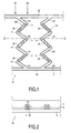
- Fig. 1 is a diagrammatic, plan view of a thermoelectric device manufactured by means of a method in accordance with the invention
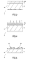
- Fig. 2 is a diagrammatic, cross-sectional view, in the thickness direction and taken on the line II-II, of the device shown in Fig. 1
- a device 10 here comprises a flexible synthetic resin foil 1 which, in this case, is strip-shaped and in which two groups 2, 3 of strip-shaped parts 2A, 3A which are series-connected via connections 4, are embedded.
- the parts 2A comprise, in this case, aluminum strips and the parts 3 A comprise monocrystalline silicon.
- the zig-zag pattern 100 of the interconnected groups 2, 3 causes the connections 4 to be alternately situated in two spaced apart areas G1, G2 of the foil.
- connections 4 can be readily introduced alternately into an area with a lower temperature and an area with a higher temperature, provided of course that such a temperature gradient is present.
- the strip-shaped semiconductor parts 3A are, in this case, further embedded between two isolating layers 8, 9 which, in this case, are made of silicon dioxide.
- the isolating layer 9 is provided with apertures in which the connections 4 between the silicon parts 3 A and the aluminum strips 2A are formed.
- the device 10 comprises a plurality of zig-zag patterns 100, 101 only two of which are shown in the drawing, and which are arranged in parallel and connected to two strip-shaped conductors 22, 23 of aluminum which are situated near an outer edge of the foil 1.
- the capacitance of the thermoelectric generator 10 is substantially increased.
- the pattern 101 is mirrored with respect to the pattern 100 with a view to folding the device 10 of this example.
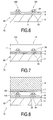
- Figs. 3 through 10 are diagrammatic, cross-sectional views at right angles to the thickness direction of the device of Fig. 1 in successive stages of the manufacture by means of an embodiment of a method in accordance with the invention.
- the manufacture of the device 10 is based (see Fig. 3 ) on the use of a monocrystalline semiconductor substrate 55 having a resistivity of 20 ⁇ cm wherein a buried isolating layer 8 is formed by implantation of oxygen ions.
- the thickness of the regions 5, 8, 55A thus formed is, in this case, 650 ⁇ m, 0.4 ⁇ m and 0.2 ⁇ m, perspectively.
- the part 55A of the silicon substrate 55 which is situated above the isolating layer 8 is heavily n-type doped by means of an ion implantation I of, in this case, arsenic ions.
- the flux of arsenic atoms is, for example, 10 16 at/cm 2 .
- the n-type-doped part is largely removed by means of photolithography and plasma etching, the strip-shaped parts 3 A being arranged in a chevron-shaped pattern that forms part of the zig-zag pattern to be formed of interconnected semiconductor strips 3A and aluminum strips that are still to be provided.
- the strip-shaped parts 3 A being arranged in a chevron-shaped pattern that forms part of the zig-zag pattern to be formed of interconnected semiconductor strips 3A and aluminum strips that are still to be provided.
- 1250 strips of silicon 3A are formed having a width of 5 ⁇ m and an interspacing of 3 ⁇ m.
- the strips 3A here extend parallel to the edges of the foil.
- a true zig-zag configuration, as shown in the Figures, is also possible however. In Figs.
- the length of the strips 3 A in this case is approximately 1 mm and the thickness is approximately 0.2 ⁇ m.
- the overall width of a zig-zag is 1250 x 8 ⁇ m is 1 cm.
- a further isolating layer 9 of silicon dioxide is formed over the mesa-shaped strips 3A (see Fig. 6 ) by means of CVD.
- the thickness of this layer 9 in this case is 0.3 ⁇ m.
- apertures of, for example, 2 ⁇ m x 2 ⁇ m are formed in the isolating layer 9 by means of photolithography and etching.
- an, in this case, 0.7 ⁇ m thick aluminum layer is deposited, in this case by means of vapor deposition, over the device 10 to be formed.
- this aluminum layer is formed into a chevron-shaped pattern of strips 2A which in conjunction with the chevron-shaped pattern of the semiconductor strips 3A forms the zig-zag structure of Fig. 1 .
- the connections 4 between the aluminum strips 2A and the silicon strips 3A are then alternately situated in two spaced apart areas indicated by means of G1 and G2 in Fig. 1 . If a temperature gradient that is present in, or applied to, the surroundings of the device 10 is presented across these areas, then the device 10 will act as a generator.
- the conductor tracks 22, 23 shown in Fig. 1 are formed at the same time from the aluminum layer.
- the patterns 100, 101 are thus incorporated in a parallel arrangement between these conductors 22, 23.
- a polyimide layer 1 is provided by means of spin coating in a thickness of in this example 10 ⁇ m, wherein, after curing, the patterns 100, 101 are embedded.
- the foil 1 thus comprises in this case a polyimide synthetic resin.
- a rigid carrier plate 6, in this case a 340 ⁇ m thick glass plate 6, is attached to the foil 1 by means of an adhesive.
- the adhesive layer 7 comprises in this case a 10 ⁇ m thick layer of HDDA mentioned in the preamble.
- the substrate part 5 is largely removed by means of grinding using a DISCO grinding machine.
- the device 10 to be formed is then situated in the grinding machine, not shown, in a mirrored orientation with respect to the adhesive layer 7, the substrate part 5 thus being situated on the upper side where the grinding process takes place.
- Approximately 600 ⁇ m of the substrate 5 are removed by grinding.
- the remaining 50 ⁇ m of the substrate part 5 are removed, in this case, by wet-chemical etching using an aqueous KOH solution, in which process the isolating layer 8 serves as an etch-stop layer.
- the foil 1 is detached from the adhesive layer 7 near an edge of the glass plate 6 using for example a scalpel. Then the foil 1 is gripped and pulled in its entirety from the glass plate 6 provided with the adhesive layer 7 using tweezers or by hand. The device 10 is now ready for further treatments, such as coiling or folding, as will be illustrated hereinbelow.
- Fig. 11 diagrammatically shows a plan view and, in part, a phantom view of a first modification of the device shown in Fig. 1 .
- the foil used in this case is a prefabricated synthetic resin foil 1 provided with holes 4.
- the semiconductor strips 3A indicated by means of interrupted lines in Fig. 11 , are formed as discussed with respect to Figs. 3 through 9 .
- the aluminum strips 2A are formed in the stage corresponding to Fig. 7 , which strips are connected to the silicon strips 3A via the apertures 4 in the foil.
- Fig. 11 only one zig-zag pattern 100 is shown.
- Fig. 12 is a diagrammatic, perspective view of the device shown in Fig. 1 , in a folded state.
- the device of Fig. 1 can be folded as shown in Fig. 12 .
- the molds are not shown in the drawing.
- the foil 1 may be provided, if necessary, with folding lines, not shown, which are situated between two neighboring patterns 100, 101.
- thermally well-conducting plates P1, P2 of, for example, copper are provided on the bottom side and on the upper side, for example, by means of a thermally well-conducting adhesive.
- these plates P1, P2 which are only partly shown in the drawing, are then introduced into a zone having, respectively, a high and a low(er) temperature.
- the power supplied by the device 10 may be drawn from external electric connection regions, not shown.
- the folded foil is further folded around a hollow pipe and is in turn surrounded by a further hollow pipe. The latter may be exposed, for example, to a medium with a lower temperature, while a medium with a higher temperature is formed by the inner hollow pipe.
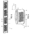
- Fig. 13 is a diagrammatic, plan view of a second modification of the device of Fig. 1 .
- Fig. 14 is a diagrammatic perspective view of the device shown in Fig. 13 , in a coiled state.
- the only difference (see Fig. 13 ) with the device of Fig. 1 is that the zig-zag patterns 100, 101 have been rotated through 90 degrees with respect to the conductor tracks 22, 23 to which the patterns 100, 101 arranged in parallel are still connected.
- two plates P1, P2 are again attached to the device 10.
- the device may comprise further active and passive semiconductor elements or electronic components, such as diodes and/or transistors and resistors and/or capacitors, whether or not in the form of an integrated circuit.
- diodes and/or transistors and resistors and/or capacitors whether or not in the form of an integrated circuit.
- a diode and a capacitor enabling temporary power storage to be realized in a simple manner would be suitable in particular. The manufacture is of course efficiently adapted thereto.
Landscapes
- Engineering & Computer Science (AREA)
- Manufacturing & Machinery (AREA)
- Weting (AREA)
- Mechanical Treatment Of Semiconductor (AREA)
- Glass Compositions (AREA)
- Transition And Organic Metals Composition Catalysts For Addition Polymerization (AREA)
Claims (10)
- Verfahren zum Herstellen einer thermoelektrischen Anordnung (10), die eine flexible Folie (1) umfasst, auf der zwei Gruppen (2, 3) von in Reihe miteinander verbundenen, streifenförmigen Teilen (2A, 3A) aufgebracht werden, wobei die für die zwei Gruppen von Teilen (2A, 3A) gewählten Materialien einen unterschiedlichen thermoelektrischen Koeffizienten haben und die genannten Gruppen von Teilen so strukturiert werden, dass die Verbindungen (4) zwischen einem Teil (2A) der einen Gruppe (2) und einem anderen Teil (3A) der anderen Gruppe (3) abwechselnd jedes Mal in einem von zwei auf Abstand voneinander liegenden Gebieten (G1, G2) der Folie (1) liegen, und wobei nach dem Aufbringen der streifenförmigen Teile (2A, 3A) auf einem Substrat (5) die Folie (1) auf den streifenförmigen Teilen (2A, 3A) aufgebracht wird, woraufhin das Substrat (5) entfernt wird, dadurch gekennzeichnet, dass für das Substrat (5) ein starres Substrat (5) genutzt wird und vor dem Entfernen des starren Substrats (5) eine starre Trägerplatte (6) an der Folie (1) befestigt wird, welche starre Trägerplatte wieder von der flexiblen Folie (1) entfernt wird, nachdem das starre Substrat (5) entfernt worden ist.
- Verfahren nach Anspruch 1, dadurch gekennzeichnet, dass zumindest der größere Teil des starren Substrats (5) mittels Schleifen entfernt wird.
- Verfahren nach Anspruch 1 oder 2, dadurch gekennzeichnet, dass die Trägerplatte (6) mit Hilfe einer Klebstoffschicht (7) an der Folie (1) befestigt wird und die Folie (1) nach dem Entfernen des Substrats (5) durch Abziehen der Folie von der Klebstoffschicht (7) entfernt wird.
- Verfahren nach Anspruch 3, dadurch gekennzeichnet, dass für das Material der Klebstoffschicht (7), 1,6-Hexandioldiacrylat (HDDA) als Klebstoff genutzt wird und für das Material der Folie (1) ein Polyimid genutzt wird.
- Verfahren nach Anspruch 1, 2, 3 oder 4, dadurch gekennzeichnet, dass für das Substrat (5) ein Halbleitersubstrat (5) genutzt wird.
- Verfahren nach Anspruch 1, 2, 3, 4 oder 5, dadurch gekennzeichnet, dass für das Material zumindest einer (3) der Gruppen (2, 3) von streifenförmigen Teilen (3A) ein Halbleitermaterial genutzt wird.
- Verfahren nach einem der vorhergehenden Ansprüche, dadurch gekennzeichnet, dass für das Substrat (5) ein monokristallines Siliciumsubstrat (5) genutzt wird, das mit einer isolierenden Schicht (8) versehen wird, auf der eine polykristalline Siliciumschicht (55A) deponiert wird.
- Verfahren nach einem der Ansprüche 1 bis 6, dadurch gekennzeichnet, dass das Substrat (5) durch den Teil eines monokristallinen Siliciumsubstrats (55), in dem mit Hilfe einer Implantation von Sauerstoffatomen eine vergrabene Oxidschicht (8) gebildet wird, der unter der Oxidschicht (8) liegt, gebildet wird.
- Verfahren nach einem der vorhergehenden Ansprüche, dadurch gekennzeichnet, dass eine Anzahl der zwei in Reihe miteinander verbundenen Gruppen (2, 3) von streifenförmigen Teilen (2A, 3A) parallel zwischen zwei streifenförmigen Leitern (22, 23) angeordnet wird, die auf der Folie (1) gebildet werden.
- Verfahren nach Anspruch 9, dadurch gekennzeichnet, dass die Folie (1) gefaltet oder aufgewickelt wird, welches Falten oder Aufwickeln in einer solchen Weise erfolgt, dass die Verbindungen (4) der zwei miteinander verbundenen Gruppen (2, 3) von streifenförmigen Teilen (2A, 3A) in zwei auf Abstand voneinander liegenden Positionen (P1, P2) bleiben.
Priority Applications (1)
| Application Number | Priority Date | Filing Date | Title |
|---|---|---|---|
| EP04733420A EP1629539B1 (de) | 2003-05-23 | 2004-05-17 | Verfahren zur herstellung einer thermoelektrischen vorrichtung |
Applications Claiming Priority (3)
| Application Number | Priority Date | Filing Date | Title |
|---|---|---|---|
| EP03101497 | 2003-05-23 | ||
| PCT/IB2004/050710 WO2004105146A1 (en) | 2003-05-23 | 2004-05-17 | Method of manufacturing a thermoelectric device and thermoelectric device obtained by means of such a method |
| EP04733420A EP1629539B1 (de) | 2003-05-23 | 2004-05-17 | Verfahren zur herstellung einer thermoelektrischen vorrichtung |
Publications (2)
| Publication Number | Publication Date |
|---|---|
| EP1629539A1 EP1629539A1 (de) | 2006-03-01 |
| EP1629539B1 true EP1629539B1 (de) | 2008-07-30 |
Family
ID=33462210
Family Applications (1)
| Application Number | Title | Priority Date | Filing Date |
|---|---|---|---|
| EP04733420A Expired - Lifetime EP1629539B1 (de) | 2003-05-23 | 2004-05-17 | Verfahren zur herstellung einer thermoelektrischen vorrichtung |
Country Status (9)
| Country | Link |
|---|---|
| US (1) | US20060278265A1 (de) |
| EP (1) | EP1629539B1 (de) |
| JP (1) | JP4098343B2 (de) |
| KR (1) | KR20060024779A (de) |
| CN (1) | CN100416878C (de) |
| AT (1) | ATE403236T1 (de) |
| DE (1) | DE602004015449D1 (de) |
| TW (1) | TW200507048A (de) |
| WO (1) | WO2004105146A1 (de) |
Families Citing this family (25)
| Publication number | Priority date | Publication date | Assignee | Title |
|---|---|---|---|---|
| US7629531B2 (en) * | 2003-05-19 | 2009-12-08 | Digital Angel Corporation | Low power thermoelectric generator |
| CA2549826C (en) | 2003-12-02 | 2014-04-08 | Battelle Memorial Institute | Thermoelectric devices and applications for the same |
| US8455751B2 (en) | 2003-12-02 | 2013-06-04 | Battelle Memorial Institute | Thermoelectric devices and applications for the same |
| US7851691B2 (en) | 2003-12-02 | 2010-12-14 | Battelle Memorial Institute | Thermoelectric devices and applications for the same |
| US7834263B2 (en) | 2003-12-02 | 2010-11-16 | Battelle Memorial Institute | Thermoelectric power source utilizing ambient energy harvesting for remote sensing and transmitting |
| WO2007002342A2 (en) * | 2005-06-22 | 2007-01-04 | Nextreme Thermal Solutions | Methods of forming thermoelectric devices including electrically insulating matrixes between conductive traces and related structures |
| US7679203B2 (en) | 2006-03-03 | 2010-03-16 | Nextreme Thermal Solutions, Inc. | Methods of forming thermoelectric devices using islands of thermoelectric material and related structures |
| US20080017238A1 (en) * | 2006-07-21 | 2008-01-24 | Caterpillar Inc. | Thermoelectric device |
| JP2008130594A (ja) * | 2006-11-16 | 2008-06-05 | Tokai Rika Co Ltd | 熱電変換デバイス及びその製造方法 |
| JP2008130813A (ja) * | 2006-11-21 | 2008-06-05 | Tokai Rika Co Ltd | 熱発電装置 |
| JP2008205129A (ja) * | 2007-02-19 | 2008-09-04 | Tokai Rika Co Ltd | 回路ブロック及びその製造方法 |
| FR2919431B1 (fr) * | 2007-07-23 | 2010-08-27 | Commissariat Energie Atomique | Moyen thermoelectrique et structure de type tissu integrant un tel moyen. |
| US20090084421A1 (en) * | 2007-09-28 | 2009-04-02 | Battelle Memorial Institute | Thermoelectric devices |
| US8198527B2 (en) | 2008-12-08 | 2012-06-12 | Perpetua Power Source Technologies, Inc. | Field-deployable electronics platform having thermoelectric power source and electronics module |
| US20110094556A1 (en) * | 2009-10-25 | 2011-04-28 | Digital Angel Corporation | Planar thermoelectric generator |
| FR2982709B1 (fr) * | 2011-11-10 | 2014-08-01 | Acome Soc Cooperative Et Participative Sa Cooperative De Production A Capital Variable | Ame thermolelectrique, structure thermoelectrique comprenant ladite ame, son procede de realisation et ses utilisations |
| WO2013114854A1 (ja) * | 2012-02-03 | 2013-08-08 | 日本電気株式会社 | 有機熱電発電素子およびその製造方法 |
| DE102012105086B4 (de) * | 2012-06-13 | 2014-02-13 | Karlsruher Institut für Technologie | Gewickeltes und gefaltetes thermoelektrisches System und Verfahren zu dessen Herstellung |
| US9064994B2 (en) | 2013-04-26 | 2015-06-23 | Eastman Chemical Company | Self-corrugating laminates useful in the manufacture of thermoelectric devices and corrugated structures therefrom |
| KR101786183B1 (ko) | 2015-07-14 | 2017-10-17 | 현대자동차주식회사 | 일체형 유연 열전소자 및 그 제조 방법 |
| CN107924981A (zh) * | 2015-08-31 | 2018-04-17 | 富士胶片株式会社 | 热电转换器件 |
| ITUB20155100A1 (it) * | 2015-10-23 | 2017-04-23 | Delta Ti Res | Generatore termoelettrico. |
| US20190181322A1 (en) * | 2016-06-23 | 2019-06-13 | 3M Innovative Properties Company | Thermoelectric tape |
| KR102047736B1 (ko) * | 2016-06-23 | 2019-11-25 | 쓰리엠 이노베이티브 프로퍼티즈 컴파니 | 가요성 열전 모듈 |
| US11832518B2 (en) | 2021-02-04 | 2023-11-28 | Purdue Research Foundation | Woven thermoelectric ribbon |
Family Cites Families (11)
| Publication number | Priority date | Publication date | Assignee | Title |
|---|---|---|---|---|
| US3770520A (en) * | 1968-06-26 | 1973-11-06 | Kyodo Denshi Gijutsu Kenkyusho | Production of semiconductor integrated-circuit devices |
| SU455702A1 (ru) * | 1973-12-06 | 1976-08-05 | Предприятие П/Я В-2763 | Термоэлемент |
| US5022928A (en) * | 1985-10-04 | 1991-06-11 | Buist Richard J | Thermoelectric heat pump/power source device |
| US5167723A (en) * | 1988-03-10 | 1992-12-01 | Yamaha Hatsudoki Kabushiki Kaisha | Thermocouple with overlapped dissimilar conductors |
| DE69511263T2 (de) * | 1994-05-16 | 2000-01-13 | Citizen Watch Co., Ltd. | Herstellung einer thermoelektrischen leistungserzeugungseinheit |
| EP1329538A2 (de) * | 1995-09-29 | 2003-07-23 | Union Material Inc. | Verfahren zur Herstellung geformter Kristalle durch Aufwärtsspritzen einer Flüssigkeit unter Druck |
| JP4903307B2 (ja) * | 1998-11-13 | 2012-03-28 | エイチアイ−ゼット・テクノロジー・インク | 極薄基板上の量子井戸熱電材料 |
| KR100313909B1 (ko) * | 1999-11-22 | 2001-11-17 | 구자홍 | 적외선 센서 및 그 제조방법 |
| US6630426B1 (en) * | 2000-01-12 | 2003-10-07 | Teracomm Research Inc. | Method of increasing the critical temperature of a high critical temperature superconducting film and a superconducting structure made using the method |
| DE10122324A1 (de) * | 2001-05-08 | 2002-11-14 | Philips Corp Intellectual Pty | Flexible integrierte monolithische Schaltung |
| JP3927784B2 (ja) * | 2001-10-24 | 2007-06-13 | 北川工業株式会社 | 熱電変換部材の製造方法 |
-
2004
- 2004-05-17 KR KR1020057022384A patent/KR20060024779A/ko not_active Ceased
- 2004-05-17 EP EP04733420A patent/EP1629539B1/de not_active Expired - Lifetime
- 2004-05-17 CN CNB2004800140942A patent/CN100416878C/zh not_active Expired - Fee Related
- 2004-05-17 AT AT04733420T patent/ATE403236T1/de not_active IP Right Cessation
- 2004-05-17 DE DE602004015449T patent/DE602004015449D1/de not_active Expired - Fee Related
- 2004-05-17 WO PCT/IB2004/050710 patent/WO2004105146A1/en not_active Ceased
- 2004-05-17 JP JP2006530862A patent/JP4098343B2/ja not_active Expired - Fee Related
- 2004-05-17 US US10/557,621 patent/US20060278265A1/en not_active Abandoned
- 2004-05-20 TW TW093114274A patent/TW200507048A/zh unknown
Also Published As
| Publication number | Publication date |
|---|---|
| JP2007511893A (ja) | 2007-05-10 |
| ATE403236T1 (de) | 2008-08-15 |
| DE602004015449D1 (de) | 2008-09-11 |
| CN1795568A (zh) | 2006-06-28 |
| US20060278265A1 (en) | 2006-12-14 |
| WO2004105146A1 (en) | 2004-12-02 |
| TW200507048A (en) | 2005-02-16 |
| EP1629539A1 (de) | 2006-03-01 |
| CN100416878C (zh) | 2008-09-03 |
| JP4098343B2 (ja) | 2008-06-11 |
| KR20060024779A (ko) | 2006-03-17 |
Similar Documents
| Publication | Publication Date | Title |
|---|---|---|
| US20060278265A1 (en) | Method of manufacturing a thermoelectric device and thermoelectric device obtained by means of such a method | |
| US9288899B2 (en) | Micro device transfer head array | |
| KR100323488B1 (ko) | 수직칩연결을위한접촉구조체 | |
| EP3118894B1 (de) | Mikrovorrichtungs-übertragungskopf mit einer siliciumelektrode | |
| US6552383B2 (en) | Integrated decoupling capacitors | |
| US9255001B2 (en) | Micro device transfer head array with metal electrodes | |
| US6291858B1 (en) | Multistack 3-dimensional high density semiconductor device and method for fabrication | |
| JPH04106932A (ja) | バイポーラトランジスタの製造方法 | |
| TW201036104A (en) | Minimum cost method for forming high density passive capacitors for replacement of discrete board capacitors using a minimum cost 3D wafer-to-wafer modular integration scheme | |
| EP0740853A1 (de) | Halbleiter mit einem träger auf dem ein substrat mit einem halbleiter-element mittels einer klebeschicht und weiteres ein leiterbahn-muster befestigt sind | |
| US10283582B2 (en) | Microelectronic circuits and integrated circuits including a non-silicon substrate | |
| TWI228753B (en) | Power generator and method for forming same | |
| CN113130621B (zh) | 具有结晶硅和富陷阱多晶硅层的晶片 | |
| US20080128868A1 (en) | Method of Transferring a Circuit Onto a Ground Plane | |
| US20170053873A1 (en) | Flexible integrated circuit devices and methods for manufacturing the same | |
| TWI726972B (zh) | 用於製造多層mems組件的方法及相應的多層mems組件 | |
| KR20020019138A (ko) | 고주파 집적회로 장치 및 그 제조 방법 | |
| CN111295745B (zh) | 用于制造多个半导体芯片的方法和半导体芯片 | |
| JP2003068854A (ja) | 配線間接続方法、配線間接続部材及びその製造方法 | |
| KR100479233B1 (ko) | 온도 센서 제조 방법 | |
| JPS6288334A (ja) | 誘電体絶縁分離基板の製造方法 | |
| KR19990052558A (ko) | 전력소자 제조 방법 및 그 구조 | |
| CN118974911A (zh) | 包括通孔的衬底及相关制造方法 | |
| JPS63126260A (ja) | 半導体集積回路の製造方法 | |
| JPH04237158A (ja) | 半導体装置およびその製造方法 |
Legal Events
| Date | Code | Title | Description |
|---|---|---|---|
| PUAI | Public reference made under article 153(3) epc to a published international application that has entered the european phase |
Free format text: ORIGINAL CODE: 0009012 |
|
| 17P | Request for examination filed |
Effective date: 20051223 |
|
| AK | Designated contracting states |
Kind code of ref document: A1 Designated state(s): AT BE BG CH CY CZ DE DK EE ES FI FR GB GR HU IE IT LI LU MC NL PL PT RO SE SI SK TR |
|
| DAX | Request for extension of the european patent (deleted) | ||
| 17Q | First examination report despatched |
Effective date: 20071120 |
|
| GRAP | Despatch of communication of intention to grant a patent |
Free format text: ORIGINAL CODE: EPIDOSNIGR1 |
|
| RTI1 | Title (correction) |
Free format text: METHOD OF MANUFACTURING A THERMOELECTRIC DEVICE |
|
| GRAS | Grant fee paid |
Free format text: ORIGINAL CODE: EPIDOSNIGR3 |
|
| GRAA | (expected) grant |
Free format text: ORIGINAL CODE: 0009210 |
|
| AK | Designated contracting states |
Kind code of ref document: B1 Designated state(s): AT BE BG CH CY CZ DE DK EE ES FI FR GB GR HU IE IT LI LU MC NL PL PT RO SE SI SK TR |
|
| REG | Reference to a national code |
Ref country code: GB Ref legal event code: FG4D |
|
| REG | Reference to a national code |
Ref country code: CH Ref legal event code: EP |
|
| REF | Corresponds to: |
Ref document number: 602004015449 Country of ref document: DE Date of ref document: 20080911 Kind code of ref document: P |
|
| REG | Reference to a national code |
Ref country code: IE Ref legal event code: FG4D |
|
| PG25 | Lapsed in a contracting state [announced via postgrant information from national office to epo] |
Ref country code: NL Free format text: LAPSE BECAUSE OF FAILURE TO SUBMIT A TRANSLATION OF THE DESCRIPTION OR TO PAY THE FEE WITHIN THE PRESCRIBED TIME-LIMIT Effective date: 20080730 Ref country code: PT Free format text: LAPSE BECAUSE OF FAILURE TO SUBMIT A TRANSLATION OF THE DESCRIPTION OR TO PAY THE FEE WITHIN THE PRESCRIBED TIME-LIMIT Effective date: 20081230 Ref country code: ES Free format text: LAPSE BECAUSE OF FAILURE TO SUBMIT A TRANSLATION OF THE DESCRIPTION OR TO PAY THE FEE WITHIN THE PRESCRIBED TIME-LIMIT Effective date: 20081110 |
|
| PG25 | Lapsed in a contracting state [announced via postgrant information from national office to epo] |
Ref country code: SI Free format text: LAPSE BECAUSE OF FAILURE TO SUBMIT A TRANSLATION OF THE DESCRIPTION OR TO PAY THE FEE WITHIN THE PRESCRIBED TIME-LIMIT Effective date: 20080730 Ref country code: BG Free format text: LAPSE BECAUSE OF FAILURE TO SUBMIT A TRANSLATION OF THE DESCRIPTION OR TO PAY THE FEE WITHIN THE PRESCRIBED TIME-LIMIT Effective date: 20081030 Ref country code: AT Free format text: LAPSE BECAUSE OF FAILURE TO SUBMIT A TRANSLATION OF THE DESCRIPTION OR TO PAY THE FEE WITHIN THE PRESCRIBED TIME-LIMIT Effective date: 20080730 Ref country code: FI Free format text: LAPSE BECAUSE OF FAILURE TO SUBMIT A TRANSLATION OF THE DESCRIPTION OR TO PAY THE FEE WITHIN THE PRESCRIBED TIME-LIMIT Effective date: 20080730 |
|
| PG25 | Lapsed in a contracting state [announced via postgrant information from national office to epo] |
Ref country code: BE Free format text: LAPSE BECAUSE OF FAILURE TO SUBMIT A TRANSLATION OF THE DESCRIPTION OR TO PAY THE FEE WITHIN THE PRESCRIBED TIME-LIMIT Effective date: 20080730 |
|
| PG25 | Lapsed in a contracting state [announced via postgrant information from national office to epo] |
Ref country code: EE Free format text: LAPSE BECAUSE OF FAILURE TO SUBMIT A TRANSLATION OF THE DESCRIPTION OR TO PAY THE FEE WITHIN THE PRESCRIBED TIME-LIMIT Effective date: 20080730 Ref country code: DK Free format text: LAPSE BECAUSE OF FAILURE TO SUBMIT A TRANSLATION OF THE DESCRIPTION OR TO PAY THE FEE WITHIN THE PRESCRIBED TIME-LIMIT Effective date: 20080730 |
|
| PG25 | Lapsed in a contracting state [announced via postgrant information from national office to epo] |
Ref country code: SK Free format text: LAPSE BECAUSE OF FAILURE TO SUBMIT A TRANSLATION OF THE DESCRIPTION OR TO PAY THE FEE WITHIN THE PRESCRIBED TIME-LIMIT Effective date: 20080730 Ref country code: CZ Free format text: LAPSE BECAUSE OF FAILURE TO SUBMIT A TRANSLATION OF THE DESCRIPTION OR TO PAY THE FEE WITHIN THE PRESCRIBED TIME-LIMIT Effective date: 20080730 Ref country code: RO Free format text: LAPSE BECAUSE OF FAILURE TO SUBMIT A TRANSLATION OF THE DESCRIPTION OR TO PAY THE FEE WITHIN THE PRESCRIBED TIME-LIMIT Effective date: 20080730 |
|
| PLBE | No opposition filed within time limit |
Free format text: ORIGINAL CODE: 0009261 |
|
| STAA | Information on the status of an ep patent application or granted ep patent |
Free format text: STATUS: NO OPPOSITION FILED WITHIN TIME LIMIT |
|
| 26N | No opposition filed |
Effective date: 20090506 |
|
| PG25 | Lapsed in a contracting state [announced via postgrant information from national office to epo] |
Ref country code: IT Free format text: LAPSE BECAUSE OF FAILURE TO SUBMIT A TRANSLATION OF THE DESCRIPTION OR TO PAY THE FEE WITHIN THE PRESCRIBED TIME-LIMIT Effective date: 20080730 |
|
| PGFP | Annual fee paid to national office [announced via postgrant information from national office to epo] |
Ref country code: FR Payment date: 20090528 Year of fee payment: 6 |
|
| PGFP | Annual fee paid to national office [announced via postgrant information from national office to epo] |
Ref country code: DE Payment date: 20090720 Year of fee payment: 6 Ref country code: GB Payment date: 20090529 Year of fee payment: 6 |
|
| PG25 | Lapsed in a contracting state [announced via postgrant information from national office to epo] |
Ref country code: MC Free format text: LAPSE BECAUSE OF NON-PAYMENT OF DUE FEES Effective date: 20090531 |
|
| REG | Reference to a national code |
Ref country code: CH Ref legal event code: PL |
|
| PG25 | Lapsed in a contracting state [announced via postgrant information from national office to epo] |
Ref country code: CH Free format text: LAPSE BECAUSE OF NON-PAYMENT OF DUE FEES Effective date: 20090531 Ref country code: LI Free format text: LAPSE BECAUSE OF NON-PAYMENT OF DUE FEES Effective date: 20090531 Ref country code: SE Free format text: LAPSE BECAUSE OF FAILURE TO SUBMIT A TRANSLATION OF THE DESCRIPTION OR TO PAY THE FEE WITHIN THE PRESCRIBED TIME-LIMIT Effective date: 20081030 |
|
| REG | Reference to a national code |
Ref country code: IE Ref legal event code: MM4A |
|
| PG25 | Lapsed in a contracting state [announced via postgrant information from national office to epo] |
Ref country code: IE Free format text: LAPSE BECAUSE OF NON-PAYMENT OF DUE FEES Effective date: 20090517 |
|
| PG25 | Lapsed in a contracting state [announced via postgrant information from national office to epo] |
Ref country code: PL Free format text: LAPSE BECAUSE OF FAILURE TO SUBMIT A TRANSLATION OF THE DESCRIPTION OR TO PAY THE FEE WITHIN THE PRESCRIBED TIME-LIMIT Effective date: 20080730 |
|
| PG25 | Lapsed in a contracting state [announced via postgrant information from national office to epo] |
Ref country code: GR Free format text: LAPSE BECAUSE OF FAILURE TO SUBMIT A TRANSLATION OF THE DESCRIPTION OR TO PAY THE FEE WITHIN THE PRESCRIBED TIME-LIMIT Effective date: 20081031 |
|
| GBPC | Gb: european patent ceased through non-payment of renewal fee |
Effective date: 20100517 |
|
| REG | Reference to a national code |
Ref country code: FR Ref legal event code: ST Effective date: 20110131 |
|
| PG25 | Lapsed in a contracting state [announced via postgrant information from national office to epo] |
Ref country code: LU Free format text: LAPSE BECAUSE OF NON-PAYMENT OF DUE FEES Effective date: 20090517 Ref country code: DE Free format text: LAPSE BECAUSE OF NON-PAYMENT OF DUE FEES Effective date: 20101201 |
|
| PG25 | Lapsed in a contracting state [announced via postgrant information from national office to epo] |
Ref country code: FR Free format text: LAPSE BECAUSE OF NON-PAYMENT OF DUE FEES Effective date: 20100531 |
|
| PG25 | Lapsed in a contracting state [announced via postgrant information from national office to epo] |
Ref country code: HU Free format text: LAPSE BECAUSE OF FAILURE TO SUBMIT A TRANSLATION OF THE DESCRIPTION OR TO PAY THE FEE WITHIN THE PRESCRIBED TIME-LIMIT Effective date: 20090131 |
|
| PG25 | Lapsed in a contracting state [announced via postgrant information from national office to epo] |
Ref country code: GB Free format text: LAPSE BECAUSE OF NON-PAYMENT OF DUE FEES Effective date: 20100517 |
|
| PG25 | Lapsed in a contracting state [announced via postgrant information from national office to epo] |
Ref country code: TR Free format text: LAPSE BECAUSE OF FAILURE TO SUBMIT A TRANSLATION OF THE DESCRIPTION OR TO PAY THE FEE WITHIN THE PRESCRIBED TIME-LIMIT Effective date: 20080730 |
|
| PG25 | Lapsed in a contracting state [announced via postgrant information from national office to epo] |
Ref country code: CY Free format text: LAPSE BECAUSE OF FAILURE TO SUBMIT A TRANSLATION OF THE DESCRIPTION OR TO PAY THE FEE WITHIN THE PRESCRIBED TIME-LIMIT Effective date: 20080730 |