EP1630652A1 - Dispositif d'entrée de coordonnées et procédé pour réduire le bruit de fond - Google Patents
Dispositif d'entrée de coordonnées et procédé pour réduire le bruit de fond Download PDFInfo
- Publication number
- EP1630652A1 EP1630652A1 EP04006834A EP04006834A EP1630652A1 EP 1630652 A1 EP1630652 A1 EP 1630652A1 EP 04006834 A EP04006834 A EP 04006834A EP 04006834 A EP04006834 A EP 04006834A EP 1630652 A1 EP1630652 A1 EP 1630652A1
- Authority
- EP
- European Patent Office
- Prior art keywords
- value
- point
- contact point
- sampling
- coordinate
- Prior art date
- Legal status (The legal status is an assumption and is not a legal conclusion. Google has not performed a legal analysis and makes no representation as to the accuracy of the status listed.)
- Granted
Links
Images


Classifications
-
- G—PHYSICS
- G06—COMPUTING OR CALCULATING; COUNTING
- G06F—ELECTRIC DIGITAL DATA PROCESSING
- G06F3/00—Input arrangements for transferring data to be processed into a form capable of being handled by the computer; Output arrangements for transferring data from processing unit to output unit, e.g. interface arrangements
- G06F3/01—Input arrangements or combined input and output arrangements for interaction between user and computer
- G06F3/03—Arrangements for converting the position or the displacement of a member into a coded form
- G06F3/041—Digitisers, e.g. for touch screens or touch pads, characterised by the transducing means
- G06F3/0416—Control or interface arrangements specially adapted for digitisers
- G06F3/0418—Control or interface arrangements specially adapted for digitisers for error correction or compensation, e.g. based on parallax, calibration or alignment
-
- G—PHYSICS
- G06—COMPUTING OR CALCULATING; COUNTING
- G06F—ELECTRIC DIGITAL DATA PROCESSING
- G06F3/00—Input arrangements for transferring data to be processed into a form capable of being handled by the computer; Output arrangements for transferring data from processing unit to output unit, e.g. interface arrangements
- G06F3/01—Input arrangements or combined input and output arrangements for interaction between user and computer
- G06F3/03—Arrangements for converting the position or the displacement of a member into a coded form
- G06F3/041—Digitisers, e.g. for touch screens or touch pads, characterised by the transducing means
- G06F3/045—Digitisers, e.g. for touch screens or touch pads, characterised by the transducing means using resistive elements, e.g. a single continuous surface or two parallel surfaces put in contact
Definitions
- the invention relates in general relates to a coordinate positioning device and the method thereof, and more particularly, to an anti-noise coordinate positioning device and the method thereof.
- Coordinate positioning devices are widely applied in man-machine interface to facilitate the communication between the user and the electronic product.
- the coordinate positioning device such as a mouse or a film positioning device for instance, detects the position and further has the position indicated on the screen by means of a cursor.
- the film positioning device which includes two pieces of resistance-type films or capacitance-type films, detects the coordinates of the contact point touched by the user.
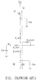
- Resistance-type film positioning device 100 includes a thin film 110.
- the thin film 110 further includes a thin film X and a thin film Y, wherein the thin film X and the thin film Y are plane resistances and have not any mutual contact in natural status.
- the resistance value on the thin film X changes along with the change of X-coordinate, not with the change of Y-coordinate, while the resistance value on the thin film Y changes along with the change of Y-coordinate, not with the change of X-coordinate.
- the thin film positioning device further includes transistors QX0, QX1, QY0, and QY1 as well as capacitances Cxp, Cxm, Cyp, and Cym for detecting the contact points and isolating the noises thereof.
- transistors QX0, QX1, QY0, and QY1 are controlled by signals X0, X1, Y0, and Y1.
- the thin film X and the thin film Y When the user touches the film positioning device 100, the thin film X and the thin film Y will be connected at a contact point whose resistance is R_touch.
- the resistance at points above the contact point is R_up
- the resistance at points below the contact point is R_down
- the resistance at points to the left of the contact point is R_left
- the resistance at points to the right of the contact point is R_right.
- the thin film positioning device 100 will obtain the Y-coordinate of the contact point according to the ratio between R_up and R_down, and will obtain the X-coordinate of the contact point according to the ratio between R_right and R_left.
- FIG. 2A is an equivalent circuit diagram for a thin film positioning device when detecting the X-coordinate of the contact point.
- transistors QY0 and QY1 are switched on, allowing an electric current I1 to reach the ground via QY1, R_left, R_right, and QY0 in succession.
- the ration between R_left and R_right will be obtained whereby the X-coordinate of the contact point can be obtained accordingly.
- the X-coordinate of the contact point can also be obtained after measuring the voltage at point XM.
- FIG. 2B is an equivalent circuit diagram for a thin film positioning device when detecting the Y-coordinate of the contact point.
- transistors QX0 and QX1 are switched on, allowing an electric current I2 to reach the ground via QX1, R_up, R_down, and QX0 in succession.
- the ration between R_up and R_down will be obtained whereby the Y-coordinate of the contact point can be obtained accordingly.
- the Y-coordinate at the contact point can also be obtained after measuring the voltage at point YM.
- a thin film positioning device When applied in an electronic device, a thin film positioning device is likely to be coupled to plenty of noises which will cause errors to the coordinates obtained. For example, despite the user presses at the same contact point, however, due to the interference of the noise, the obtained coordinates of the contact point may be changeable.
- the general practice is to have multiple samplings of the contact point, say, 8 samplings, within a specific period of time, then use the average values of the 8 samplings as the coordinates of the contact point.
- using multiple sampling to determine the coordinates of the contact point is both time-consuming and energy consuming.
- a positioning method is provided to be applied in a thin film positioning device for detecting the coordinates of a contact point even in an environment of periodic noises.
- the steps of the positioning method are disclosed below. Firstly, obtain a first sampling value of the contact point at a first time point and a second sampling value of the contact point at a second time point in succession. Next, determine if the absolute value of the difference between the first sampling value and the second sampling value is smaller than a first threshold value or not. If not, neglect this contact point and end the process of this method; if yes, obtain a third sampling value of the contact point at a third time point.
- FIG. 1 is a circuit diagram of a resistance-type film positioning device
- FIG. 2A is an equivalent circuit diagram for a thin film positioning device when detecting the X-coordinate of the contact
- FIG. 2B is an equivalent circuit diagram for a thin film positioning device when detecting the Y-coordinate of the contact point
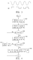
- FIG. 3 is a schematic diagram of periodic noises
- FIG. 4 is a flowchart of a positioning method according to a preferred embodiment of the invention.
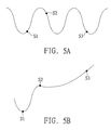
- FIG. 5A and FIG. 5B are voltage diagrams for point XP.
- FIG. 3 is a schematic diagram of periodic noises.
- the film positioning device 100 of an electronic device are likely to be coupled to noises such as sine wave noises N1 or square wave noises N2.
- the thin film positioning device according to the invention can promptly and precisely position the coordinates of the contact point under the circumstance of periodic noises.
- FIG. 4 a flowchart of a positioning method according to a preferred embodiment of the invention.
- T be the period of periodic noises.
- the voltage at point XP, point XM, point YP or point YM of the thin film positioning device 100 is sampled and measured.
- point XP is used as an example of explanation. Having taken the voltage value of the sampled point XP, the ration between R_right and R_left will be obtained whereby the X-coordinate of the contact point can be referred.
- FIG. 5A and FIG. 5B voltage diagrams for point XP.
- the voltage value at point XP will show a periodic pattern as well. Firstly, obtain a first sampling value S1 of point XP at a first time point as shown in step 410. Next, obtain a second sampling value S2 of point XP at a second time point as shown in step 420. The interval between the first time point and the second time point is roughly a half of the noise period T.
- the average of the first sampling value S1 and the second sampling value S2 can be regarded as the voltage value of point XP.
- the voltage at point XP sometimes shows an irregular pattern due to the sudden change of the noise. If this is the case, the average of the first sampling value and the second sampling value cannot be seen as the voltage value of point XP and a further check is required.
- step 430 Determine if the absolute value of the difference between the first sampling value S1 and the second sampling value S2 is smaller than a first threshold value H1 or not as shown in step 430: if not, proceed to step 435 and neglect the present contact point because the above samplings fail to represent the actual point touched by the user.
- step 440 considering the voltage at point XP might surge up if the user applies too weak a force, so a further check is conducted in step 440. If the user applies too weak a force at the positioning device 100, the resistance at R_touch will surge up. Referring to FIG. 2A, if the electricity of capacitance Cxp has not been fully discharged, a small current will flow through R_touch causing the voltage at point XP to surge up as shown in FIG. 5B.
- a third sampling value is obtained at a third time point.
- the interval between the first time point and the third time point is roughly a multiple of T, the period of the periodic noise.
- step 450 determines if the absolute value of the difference between S1and S3 is smaller than a second threshold value H2 or not: if yes, the average value of S1 and S2 is used as the sampling value of point XP to obtain the X-coordinate of point XP accordingly; if not, proceed to step 435 and neglect the contact point.
- sampling value S3 should be much the same as sampling value S1 while threshold value H2 should be smaller than threshold value H1.
- S3 will surge up as shown in FIG. 5B. If this is the case, this contact point should be neglected as if the user did not touch the positioning device at all.
- the above disclosure uses the detection of the voltage at point XP as an example. However, the above procedures can also be applied to the detection of the voltage at points YP, YM, or XM as well. With only three samplings, the invention can promptly obtain the X-coordinate or the Y-coordinate of the contact point under an environment of periodic noises, avoiding the error of estimate due to the instant instability of the noise and due to too weak a force is applied at the contact point, thereby having the advantages of both promptness and preciseness.
Landscapes
- Engineering & Computer Science (AREA)
- General Engineering & Computer Science (AREA)
- Theoretical Computer Science (AREA)
- Human Computer Interaction (AREA)
- Physics & Mathematics (AREA)
- General Physics & Mathematics (AREA)
- Position Input By Displaying (AREA)
Priority Applications (2)
| Application Number | Priority Date | Filing Date | Title |
|---|---|---|---|
| EP04006834A EP1630652B1 (fr) | 2004-03-22 | 2004-03-22 | Dispositif d'entrée de coordonnées et procédé pour réduire le bruit de fond |
| DE602004028365T DE602004028365D1 (de) | 2004-03-22 | 2004-03-22 | Koordinateneingabegerät mit Verfahren zur Unterdrückung von Rauschen |
Applications Claiming Priority (1)
| Application Number | Priority Date | Filing Date | Title |
|---|---|---|---|
| EP04006834A EP1630652B1 (fr) | 2004-03-22 | 2004-03-22 | Dispositif d'entrée de coordonnées et procédé pour réduire le bruit de fond |
Publications (2)
| Publication Number | Publication Date |
|---|---|
| EP1630652A1 true EP1630652A1 (fr) | 2006-03-01 |
| EP1630652B1 EP1630652B1 (fr) | 2010-07-28 |
Family
ID=34924521
Family Applications (1)
| Application Number | Title | Priority Date | Filing Date |
|---|---|---|---|
| EP04006834A Expired - Lifetime EP1630652B1 (fr) | 2004-03-22 | 2004-03-22 | Dispositif d'entrée de coordonnées et procédé pour réduire le bruit de fond |
Country Status (2)
| Country | Link |
|---|---|
| EP (1) | EP1630652B1 (fr) |
| DE (1) | DE602004028365D1 (fr) |
Cited By (7)
| Publication number | Priority date | Publication date | Assignee | Title |
|---|---|---|---|---|
| WO2011041941A1 (fr) * | 2009-10-09 | 2011-04-14 | 禾瑞亚科技股份有限公司 | Procédé et appareil de conversion d'informations de détection |
| US8400423B2 (en) | 2009-10-09 | 2013-03-19 | Egalax—Empia Technology Inc. | Method and device for analyzing positions |
| US8471826B2 (en) | 2009-10-09 | 2013-06-25 | Egalax—Empia Technology Inc. | Method and device for position detection |
| US8587555B2 (en) | 2009-10-09 | 2013-11-19 | Egalax—Empia Technology Inc. | Method and device for capacitive position detection |
| US8872776B2 (en) | 2009-10-09 | 2014-10-28 | Egalax—Empia Technology Inc. | Method and device for analyzing two-dimension sensing information |
| US9285940B2 (en) | 2009-10-09 | 2016-03-15 | Egalax—Empia Technology Inc. | Method and device for position detection |
| US9864471B2 (en) | 2009-10-09 | 2018-01-09 | Egalax_Empia Technology Inc. | Method and processor for analyzing two-dimension information |
Families Citing this family (1)
| Publication number | Priority date | Publication date | Assignee | Title |
|---|---|---|---|---|
| EP2503432A4 (fr) | 2009-10-09 | 2014-07-23 | Egalax Empia Technology Inc | Procédé et dispositif de détection différentielle double |
Citations (7)
| Publication number | Priority date | Publication date | Assignee | Title |
|---|---|---|---|---|
| JPH0383113A (ja) * | 1989-08-28 | 1991-04-09 | Sharp Corp | 座標検出装置 |
| JPH0816304A (ja) * | 1994-06-29 | 1996-01-19 | Nec Home Electron Ltd | タブレット装置 |
| JPH0944308A (ja) * | 1995-07-31 | 1997-02-14 | Zanavy Informatics:Kk | タッチパネル制御装置 |
| US5831599A (en) * | 1993-08-31 | 1998-11-03 | Alps Electric Co., Ltd. | Coordinate input apparatus |
| JP2001306259A (ja) * | 2000-04-20 | 2001-11-02 | Nec Infrontia Corp | タッチパネルスキャン方式 |
| US6366866B1 (en) | 1998-01-27 | 2002-04-02 | Sanyo Electric Co., Ltd. | Coordinates detecting apparatus for independently correcting coordinates |
| JP2003091365A (ja) * | 2001-09-19 | 2003-03-28 | Sharp Corp | 座標入力装置 |
-
2004
- 2004-03-22 DE DE602004028365T patent/DE602004028365D1/de not_active Expired - Lifetime
- 2004-03-22 EP EP04006834A patent/EP1630652B1/fr not_active Expired - Lifetime
Patent Citations (7)
| Publication number | Priority date | Publication date | Assignee | Title |
|---|---|---|---|---|
| JPH0383113A (ja) * | 1989-08-28 | 1991-04-09 | Sharp Corp | 座標検出装置 |
| US5831599A (en) * | 1993-08-31 | 1998-11-03 | Alps Electric Co., Ltd. | Coordinate input apparatus |
| JPH0816304A (ja) * | 1994-06-29 | 1996-01-19 | Nec Home Electron Ltd | タブレット装置 |
| JPH0944308A (ja) * | 1995-07-31 | 1997-02-14 | Zanavy Informatics:Kk | タッチパネル制御装置 |
| US6366866B1 (en) | 1998-01-27 | 2002-04-02 | Sanyo Electric Co., Ltd. | Coordinates detecting apparatus for independently correcting coordinates |
| JP2001306259A (ja) * | 2000-04-20 | 2001-11-02 | Nec Infrontia Corp | タッチパネルスキャン方式 |
| JP2003091365A (ja) * | 2001-09-19 | 2003-03-28 | Sharp Corp | 座標入力装置 |
Non-Patent Citations (5)
| Title |
|---|
| PATENT ABSTRACTS OF JAPAN vol. 015, no. 255 (P - 1221) 27 June 1991 (1991-06-27) * |
| PATENT ABSTRACTS OF JAPAN vol. 1996, no. 05 31 May 1996 (1996-05-31) * |
| PATENT ABSTRACTS OF JAPAN vol. 1997, no. 06 30 June 1997 (1997-06-30) * |
| PATENT ABSTRACTS OF JAPAN vol. 2002, no. 03 3 April 2002 (2002-04-03) * |
| PATENT ABSTRACTS OF JAPAN vol. 2003, no. 07 3 July 2003 (2003-07-03) * |
Cited By (27)
| Publication number | Priority date | Publication date | Assignee | Title |
|---|---|---|---|---|
| WO2011041941A1 (fr) * | 2009-10-09 | 2011-04-14 | 禾瑞亚科技股份有限公司 | Procédé et appareil de conversion d'informations de détection |
| US8400423B2 (en) | 2009-10-09 | 2013-03-19 | Egalax—Empia Technology Inc. | Method and device for analyzing positions |
| US8400422B2 (en) | 2009-10-09 | 2013-03-19 | Egalax—Empia Technology Inc. | Method and device for analyzing positions |
| US8400424B2 (en) | 2009-10-09 | 2013-03-19 | Egalax—Empia Technology Inc. | Method and device for analyzing positions |
| US8400425B2 (en) | 2009-10-09 | 2013-03-19 | Egalax—Empia Technology Inc. | Method and device for analyzing positions |
| US8471826B2 (en) | 2009-10-09 | 2013-06-25 | Egalax—Empia Technology Inc. | Method and device for position detection |
| US8473243B2 (en) | 2009-10-09 | 2013-06-25 | Egalax—Empia Technology Inc. | Method and device for analyzing positions |
| US8497851B2 (en) | 2009-10-09 | 2013-07-30 | Egalax—Empia Technology Inc. | Method and device for analyzing positions |
| US8537131B2 (en) | 2009-10-09 | 2013-09-17 | Egalax—Empia Technology Inc. | Method and device for converting sensing information |
| US8564564B2 (en) | 2009-10-09 | 2013-10-22 | Egalax—Empia Technology Inc. | Method and device for position detection |
| US8570289B2 (en) | 2009-10-09 | 2013-10-29 | Egalax—Empia Technology Inc. | Method and device for position detection |
| US8587555B2 (en) | 2009-10-09 | 2013-11-19 | Egalax—Empia Technology Inc. | Method and device for capacitive position detection |
| US8633917B2 (en) | 2009-10-09 | 2014-01-21 | Egalax—Empia Technology Inc. | Method and device for capacitive position detection |
| US8872776B2 (en) | 2009-10-09 | 2014-10-28 | Egalax—Empia Technology Inc. | Method and device for analyzing two-dimension sensing information |
| US8896548B2 (en) | 2009-10-09 | 2014-11-25 | Egalax—Empia Technology Inc. | Capacitive touch screen with method and device for converting sensing information including zero cross point |
| US8941597B2 (en) | 2009-10-09 | 2015-01-27 | Egalax—Empia Technology Inc. | Method and device for analyzing two-dimension sensing information |
| US8970551B2 (en) | 2009-10-09 | 2015-03-03 | Egalax—Empia Technology Inc. | Method and device for position detection |
| US8970552B2 (en) | 2009-10-09 | 2015-03-03 | Egalax—Empia Technology Inc. | Method and device for position detection |
| US9069410B2 (en) | 2009-10-09 | 2015-06-30 | Egalax—Empia Technology Inc. | Method and device for analyzing two-dimension sensing information |
| US9081441B2 (en) | 2009-10-09 | 2015-07-14 | Egalax—Empia Technology Inc. | Method and device for analyzing two-dimension sensing information |
| US9285940B2 (en) | 2009-10-09 | 2016-03-15 | Egalax—Empia Technology Inc. | Method and device for position detection |
| US9606692B2 (en) | 2009-10-09 | 2017-03-28 | Egalax_Empia Technology Inc. | Controller for position detection |
| US9798427B2 (en) | 2009-10-09 | 2017-10-24 | Egalax_Empia Technology Inc. | Method and device for dual-differential sensing |
| US9864471B2 (en) | 2009-10-09 | 2018-01-09 | Egalax_Empia Technology Inc. | Method and processor for analyzing two-dimension information |
| US9977556B2 (en) | 2009-10-09 | 2018-05-22 | Egalax_Empia Technology Inc. | Controller for position detection |
| US10101372B2 (en) | 2009-10-09 | 2018-10-16 | Egalax_Empia Technology Inc. | Method and device for analyzing positions |
| US10310693B2 (en) | 2009-10-09 | 2019-06-04 | Egalax_Empia Technology Inc. | Controller for position detection |
Also Published As
| Publication number | Publication date |
|---|---|
| EP1630652B1 (fr) | 2010-07-28 |
| DE602004028365D1 (de) | 2010-09-09 |
Similar Documents
| Publication | Publication Date | Title |
|---|---|---|
| US7301525B2 (en) | Coordinate positioning device and method thereof | |
| US8952892B2 (en) | Input location correction tables for input panels | |
| US20070268272A1 (en) | Variable capacitor array | |
| CN105045445B (zh) | 用于噪声测量的驱动传感器电极 | |
| US20130234977A1 (en) | Calibration for pressure effects on touch sensor panels | |
| US9921668B1 (en) | Touch panel controller integrated with host processor for dynamic baseline image update | |
| EP2290511A2 (fr) | Panneau tactile et procédé de localisation d'un point touché sur celui-ci | |
| US20140160038A1 (en) | Touch sensing method and touch sensing apparatus | |
| WO2006115946A2 (fr) | Dispositif et procede tactiles mettant en application une information pre-tactile | |
| CN106445235A (zh) | 一种触摸起始位置识别方法及移动终端 | |
| US9152255B2 (en) | Management and application methods and systems for touch-sensitive devices, and computer program products thereof | |
| EP1630652A1 (fr) | Dispositif d'entrée de coordonnées et procédé pour réduire le bruit de fond | |
| US12474803B2 (en) | Correcting touch interference for active pen | |
| US20140139478A1 (en) | Touch sensing method and touch sensing device | |
| JP2019207682A (ja) | ノイズ抑制回路 | |
| US9864467B2 (en) | Calibration method and capacitive sensing device | |
| CN104487924B (zh) | 触摸输入设备控制装置、以及触摸输入设备控制方法 | |
| CN101866252A (zh) | 电容式触摸装置的防水方法 | |
| CN104185832A (zh) | 触摸屏系统 | |
| US9465500B2 (en) | Two-touch gesture detection on a four-wire resistive touchscreen | |
| KR20090072347A (ko) | 하이브리드 터치스크린을 구비한 단말 장치 및 그 제어방법 | |
| US10540042B2 (en) | Impedance ratio-based current conveyor | |
| US20140168112A1 (en) | Touch sensing method and touch sensing apparatus | |
| CN100435072C (zh) | 坐标定位装置及其方法 | |
| TWI412961B (zh) | 觸摸屏之控制裝置及控制方法 |
Legal Events
| Date | Code | Title | Description |
|---|---|---|---|
| PUAI | Public reference made under article 153(3) epc to a published international application that has entered the european phase |
Free format text: ORIGINAL CODE: 0009012 |
|
| AK | Designated contracting states |
Kind code of ref document: A1 Designated state(s): AT BE BG CH CY CZ DE DK EE ES FI FR GB GR HU IE IT LI LU MC NL PL PT RO SE SI SK TR |
|
| AX | Request for extension of the european patent |
Extension state: AL LT LV MK |
|
| 17P | Request for examination filed |
Effective date: 20060301 |
|
| AKX | Designation fees paid |
Designated state(s): DE FR GB |
|
| 17Q | First examination report despatched |
Effective date: 20070130 |
|
| GRAP | Despatch of communication of intention to grant a patent |
Free format text: ORIGINAL CODE: EPIDOSNIGR1 |
|
| RIC1 | Information provided on ipc code assigned before grant |
Ipc: G06F 3/041 20060101AFI20100202BHEP |
|
| RAP1 | Party data changed (applicant data changed or rights of an application transferred) |
Owner name: HTC CORPORATION |
|
| GRAS | Grant fee paid |
Free format text: ORIGINAL CODE: EPIDOSNIGR3 |
|
| GRAA | (expected) grant |
Free format text: ORIGINAL CODE: 0009210 |
|
| AK | Designated contracting states |
Kind code of ref document: B1 Designated state(s): DE FR GB |
|
| REG | Reference to a national code |
Ref country code: GB Ref legal event code: FG4D |
|
| REF | Corresponds to: |
Ref document number: 602004028365 Country of ref document: DE Date of ref document: 20100909 Kind code of ref document: P |
|
| PLBE | No opposition filed within time limit |
Free format text: ORIGINAL CODE: 0009261 |
|
| STAA | Information on the status of an ep patent application or granted ep patent |
Free format text: STATUS: NO OPPOSITION FILED WITHIN TIME LIMIT |
|
| 26N | No opposition filed |
Effective date: 20110429 |
|
| REG | Reference to a national code |
Ref country code: DE Ref legal event code: R097 Ref document number: 602004028365 Country of ref document: DE Effective date: 20110429 |
|
| REG | Reference to a national code |
Ref country code: FR Ref legal event code: PLFP Year of fee payment: 13 |
|
| REG | Reference to a national code |
Ref country code: FR Ref legal event code: PLFP Year of fee payment: 14 |
|
| REG | Reference to a national code |
Ref country code: FR Ref legal event code: PLFP Year of fee payment: 15 |
|
| PGFP | Annual fee paid to national office [announced via postgrant information from national office to epo] |
Ref country code: GB Payment date: 20180321 Year of fee payment: 15 Ref country code: DE Payment date: 20180306 Year of fee payment: 15 |
|
| PGFP | Annual fee paid to national office [announced via postgrant information from national office to epo] |
Ref country code: FR Payment date: 20190213 Year of fee payment: 16 |
|
| REG | Reference to a national code |
Ref country code: DE Ref legal event code: R119 Ref document number: 602004028365 Country of ref document: DE |
|
| GBPC | Gb: european patent ceased through non-payment of renewal fee |
Effective date: 20190322 |
|
| PG25 | Lapsed in a contracting state [announced via postgrant information from national office to epo] |
Ref country code: DE Free format text: LAPSE BECAUSE OF NON-PAYMENT OF DUE FEES Effective date: 20191001 Ref country code: GB Free format text: LAPSE BECAUSE OF NON-PAYMENT OF DUE FEES Effective date: 20190322 |
|
| PG25 | Lapsed in a contracting state [announced via postgrant information from national office to epo] |
Ref country code: FR Free format text: LAPSE BECAUSE OF NON-PAYMENT OF DUE FEES Effective date: 20200331 |