EP1630842A2 - Elektronenemitter - Google Patents
Elektronenemitter Download PDFInfo
- Publication number
- EP1630842A2 EP1630842A2 EP05255199A EP05255199A EP1630842A2 EP 1630842 A2 EP1630842 A2 EP 1630842A2 EP 05255199 A EP05255199 A EP 05255199A EP 05255199 A EP05255199 A EP 05255199A EP 1630842 A2 EP1630842 A2 EP 1630842A2
- Authority
- EP
- European Patent Office
- Prior art keywords
- emitter
- electrode
- following
- emitter section
- electron emitter
- Prior art date
- Legal status (The legal status is an assumption and is not a legal conclusion. Google has not performed a legal analysis and makes no representation as to the accuracy of the status listed.)
- Granted
Links
- 239000000203 mixture Substances 0.000 claims abstract description 173
- 230000005684 electric field Effects 0.000 claims abstract description 59
- 239000000758 substrate Substances 0.000 claims abstract description 52
- 239000003989 dielectric material Substances 0.000 claims abstract description 22
- 239000013078 crystal Substances 0.000 claims description 57
- 229910052758 niobium Inorganic materials 0.000 claims description 33
- NUJOXMJBOLGQSY-UHFFFAOYSA-N manganese dioxide Chemical compound O=[Mn]=O NUJOXMJBOLGQSY-UHFFFAOYSA-N 0.000 claims description 24
- 229910052750 molybdenum Inorganic materials 0.000 claims description 19
- 229910052715 tantalum Inorganic materials 0.000 claims description 19
- 229910052721 tungsten Inorganic materials 0.000 claims description 16
- 229910052712 strontium Inorganic materials 0.000 claims description 15
- 229910052746 lanthanum Inorganic materials 0.000 claims description 13
- 229910052797 bismuth Inorganic materials 0.000 claims description 10
- 230000009467 reduction Effects 0.000 abstract description 15
- 230000001629 suppression Effects 0.000 abstract description 3
- 239000010936 titanium Substances 0.000 description 63
- 239000011133 lead Substances 0.000 description 50
- 238000012360 testing method Methods 0.000 description 36
- 239000003990 capacitor Substances 0.000 description 35
- 239000000463 material Substances 0.000 description 31
- 239000011777 magnesium Substances 0.000 description 29
- 230000000052 comparative effect Effects 0.000 description 25
- 238000006467 substitution reaction Methods 0.000 description 24
- 230000010287 polarization Effects 0.000 description 22
- 238000000034 method Methods 0.000 description 20
- 239000002245 particle Substances 0.000 description 20
- 229910052749 magnesium Inorganic materials 0.000 description 17
- RKTYLMNFRDHKIL-UHFFFAOYSA-N copper;5,10,15,20-tetraphenylporphyrin-22,24-diide Chemical group [Cu+2].C1=CC(C(=C2C=CC([N-]2)=C(C=2C=CC=CC=2)C=2C=CC(N=2)=C(C=2C=CC=CC=2)C2=CC=C3[N-]2)C=2C=CC=CC=2)=NC1=C3C1=CC=CC=C1 RKTYLMNFRDHKIL-UHFFFAOYSA-N 0.000 description 12
- RVTZCBVAJQQJTK-UHFFFAOYSA-N oxygen(2-);zirconium(4+) Chemical compound [O-2].[O-2].[Zr+4] RVTZCBVAJQQJTK-UHFFFAOYSA-N 0.000 description 12
- 229910001928 zirconium oxide Inorganic materials 0.000 description 12
- 239000010408 film Substances 0.000 description 11
- BASFCYQUMIYNBI-UHFFFAOYSA-N platinum Chemical compound [Pt] BASFCYQUMIYNBI-UHFFFAOYSA-N 0.000 description 11
- 230000008707 rearrangement Effects 0.000 description 11
- VZSRBBMJRBPUNF-UHFFFAOYSA-N 2-(2,3-dihydro-1H-inden-2-ylamino)-N-[3-oxo-3-(2,4,6,7-tetrahydrotriazolo[4,5-c]pyridin-5-yl)propyl]pyrimidine-5-carboxamide Chemical compound C1C(CC2=CC=CC=C12)NC1=NC=C(C=N1)C(=O)NCCC(N1CC2=C(CC1)NN=N2)=O VZSRBBMJRBPUNF-UHFFFAOYSA-N 0.000 description 10
- 239000011575 calcium Substances 0.000 description 10
- 238000011156 evaluation Methods 0.000 description 10
- 238000004519 manufacturing process Methods 0.000 description 10
- 238000007650 screen-printing Methods 0.000 description 9
- 229910019653 Mg1/3Nb2/3 Inorganic materials 0.000 description 8
- MCMNRKCIXSYSNV-UHFFFAOYSA-N Zirconium dioxide Chemical compound O=[Zr]=O MCMNRKCIXSYSNV-UHFFFAOYSA-N 0.000 description 8
- 230000007423 decrease Effects 0.000 description 8
- 230000006866 deterioration Effects 0.000 description 8
- 238000010586 diagram Methods 0.000 description 8
- 230000000694 effects Effects 0.000 description 8
- 238000010438 heat treatment Methods 0.000 description 8
- 239000013528 metallic particle Substances 0.000 description 8
- 230000002093 peripheral effect Effects 0.000 description 8
- 238000007669 thermal treatment Methods 0.000 description 8
- 239000000843 powder Substances 0.000 description 7
- CPLXHLVBOLITMK-UHFFFAOYSA-N Magnesium oxide Chemical compound [Mg]=O CPLXHLVBOLITMK-UHFFFAOYSA-N 0.000 description 6
- 230000007547 defect Effects 0.000 description 6
- 239000010419 fine particle Substances 0.000 description 6
- 239000002994 raw material Substances 0.000 description 6
- 239000006104 solid solution Substances 0.000 description 6
- 229910052719 titanium Inorganic materials 0.000 description 6
- DEXFNLNNUZKHNO-UHFFFAOYSA-N 6-[3-[4-[2-(2,3-dihydro-1H-inden-2-ylamino)pyrimidin-5-yl]piperidin-1-yl]-3-oxopropyl]-3H-1,3-benzoxazol-2-one Chemical compound C1C(CC2=CC=CC=C12)NC1=NC=C(C=N1)C1CCN(CC1)C(CCC1=CC2=C(NC(O2)=O)C=C1)=O DEXFNLNNUZKHNO-UHFFFAOYSA-N 0.000 description 5
- GWEVSGVZZGPLCZ-UHFFFAOYSA-N Titan oxide Chemical compound O=[Ti]=O GWEVSGVZZGPLCZ-UHFFFAOYSA-N 0.000 description 5
- 229910045601 alloy Inorganic materials 0.000 description 5
- 239000000956 alloy Substances 0.000 description 5
- 230000008859 change Effects 0.000 description 5
- 229910052745 lead Inorganic materials 0.000 description 5
- 230000004048 modification Effects 0.000 description 5
- 238000012986 modification Methods 0.000 description 5
- 230000008569 process Effects 0.000 description 5
- KDLHZDBZIXYQEI-UHFFFAOYSA-N Palladium Chemical compound [Pd] KDLHZDBZIXYQEI-UHFFFAOYSA-N 0.000 description 4
- OAICVXFJPJFONN-UHFFFAOYSA-N Phosphorus Chemical compound [P] OAICVXFJPJFONN-UHFFFAOYSA-N 0.000 description 4
- 230000015572 biosynthetic process Effects 0.000 description 4
- 229910010293 ceramic material Inorganic materials 0.000 description 4
- 239000012141 concentrate Substances 0.000 description 4
- 239000011521 glass Substances 0.000 description 4
- 230000006872 improvement Effects 0.000 description 4
- 239000000395 magnesium oxide Substances 0.000 description 4
- 229910052751 metal Inorganic materials 0.000 description 4
- ZKATWMILCYLAPD-UHFFFAOYSA-N niobium pentoxide Chemical compound O=[Nb](=O)O[Nb](=O)=O ZKATWMILCYLAPD-UHFFFAOYSA-N 0.000 description 4
- SIWVEOZUMHYXCS-UHFFFAOYSA-N oxo(oxoyttriooxy)yttrium Chemical compound O=[Y]O[Y]=O SIWVEOZUMHYXCS-UHFFFAOYSA-N 0.000 description 4
- 229910052697 platinum Inorganic materials 0.000 description 4
- 229910052726 zirconium Inorganic materials 0.000 description 4
- YLZOPXRUQYQQID-UHFFFAOYSA-N 3-(2,4,6,7-tetrahydrotriazolo[4,5-c]pyridin-5-yl)-1-[4-[2-[[3-(trifluoromethoxy)phenyl]methylamino]pyrimidin-5-yl]piperazin-1-yl]propan-1-one Chemical compound N1N=NC=2CN(CCC=21)CCC(=O)N1CCN(CC1)C=1C=NC(=NC=1)NCC1=CC(=CC=C1)OC(F)(F)F YLZOPXRUQYQQID-UHFFFAOYSA-N 0.000 description 3
- OKTJSMMVPCPJKN-UHFFFAOYSA-N Carbon Chemical compound [C] OKTJSMMVPCPJKN-UHFFFAOYSA-N 0.000 description 3
- 150000004649 carbonic acid derivatives Chemical class 0.000 description 3
- 238000005229 chemical vapour deposition Methods 0.000 description 3
- 239000011248 coating agent Substances 0.000 description 3
- 238000000576 coating method Methods 0.000 description 3
- 238000001816 cooling Methods 0.000 description 3
- 238000000280 densification Methods 0.000 description 3
- 238000010894 electron beam technology Methods 0.000 description 3
- ZBSCCQXBYNSKPV-UHFFFAOYSA-N oxolead;oxomagnesium;2,4,5-trioxa-1$l^{5},3$l^{5}-diniobabicyclo[1.1.1]pentane 1,3-dioxide Chemical compound [Mg]=O.[Pb]=O.[Pb]=O.[Pb]=O.O1[Nb]2(=O)O[Nb]1(=O)O2 ZBSCCQXBYNSKPV-UHFFFAOYSA-N 0.000 description 3
- 238000005245 sintering Methods 0.000 description 3
- 238000004544 sputter deposition Methods 0.000 description 3
- 239000003381 stabilizer Substances 0.000 description 3
- 230000009466 transformation Effects 0.000 description 3
- BQCADISMDOOEFD-UHFFFAOYSA-N Silver Chemical compound [Ag] BQCADISMDOOEFD-UHFFFAOYSA-N 0.000 description 2
- 239000011230 binding agent Substances 0.000 description 2
- 229910052799 carbon Inorganic materials 0.000 description 2
- 150000001875 compounds Chemical class 0.000 description 2
- 238000000151 deposition Methods 0.000 description 2
- 238000007598 dipping method Methods 0.000 description 2
- 230000002349 favourable effect Effects 0.000 description 2
- PCHJSUWPFVWCPO-UHFFFAOYSA-N gold Chemical compound [Au] PCHJSUWPFVWCPO-UHFFFAOYSA-N 0.000 description 2
- 229910052737 gold Inorganic materials 0.000 description 2
- 239000010931 gold Substances 0.000 description 2
- AMGQUBHHOARCQH-UHFFFAOYSA-N indium;oxotin Chemical compound [In].[Sn]=O AMGQUBHHOARCQH-UHFFFAOYSA-N 0.000 description 2
- 238000007733 ion plating Methods 0.000 description 2
- 238000010884 ion-beam technique Methods 0.000 description 2
- YEXPOXQUZXUXJW-UHFFFAOYSA-N lead(II) oxide Inorganic materials [Pb]=O YEXPOXQUZXUXJW-UHFFFAOYSA-N 0.000 description 2
- XMFOQHDPRMAJNU-UHFFFAOYSA-N lead(II,IV) oxide Inorganic materials O1[Pb]O[Pb]11O[Pb]O1 XMFOQHDPRMAJNU-UHFFFAOYSA-N 0.000 description 2
- AXZKOIWUVFPNLO-UHFFFAOYSA-N magnesium;oxygen(2-) Chemical compound [O-2].[Mg+2] AXZKOIWUVFPNLO-UHFFFAOYSA-N 0.000 description 2
- 239000002184 metal Substances 0.000 description 2
- 238000003801 milling Methods 0.000 description 2
- 229910052759 nickel Inorganic materials 0.000 description 2
- TWNQGVIAIRXVLR-UHFFFAOYSA-N oxo(oxoalumanyloxy)alumane Chemical compound O=[Al]O[Al]=O TWNQGVIAIRXVLR-UHFFFAOYSA-N 0.000 description 2
- 229910052763 palladium Inorganic materials 0.000 description 2
- 238000007747 plating Methods 0.000 description 2
- 230000001105 regulatory effect Effects 0.000 description 2
- 229910052703 rhodium Inorganic materials 0.000 description 2
- 239000010948 rhodium Substances 0.000 description 2
- MHOVAHRLVXNVSD-UHFFFAOYSA-N rhodium atom Chemical compound [Rh] MHOVAHRLVXNVSD-UHFFFAOYSA-N 0.000 description 2
- 229910052709 silver Inorganic materials 0.000 description 2
- 239000004332 silver Substances 0.000 description 2
- 230000026683 transduction Effects 0.000 description 2
- 238000010361 transduction Methods 0.000 description 2
- 238000007738 vacuum evaporation Methods 0.000 description 2
- 238000007740 vapor deposition Methods 0.000 description 2
- YIWGJFPJRAEKMK-UHFFFAOYSA-N 1-(2H-benzotriazol-5-yl)-3-methyl-8-[2-[[3-(trifluoromethoxy)phenyl]methylamino]pyrimidine-5-carbonyl]-1,3,8-triazaspiro[4.5]decane-2,4-dione Chemical compound CN1C(=O)N(c2ccc3n[nH]nc3c2)C2(CCN(CC2)C(=O)c2cnc(NCc3cccc(OC(F)(F)F)c3)nc2)C1=O YIWGJFPJRAEKMK-UHFFFAOYSA-N 0.000 description 1
- ZOKXTWBITQBERF-UHFFFAOYSA-N Molybdenum Chemical compound [Mo] ZOKXTWBITQBERF-UHFFFAOYSA-N 0.000 description 1
- 229910001252 Pd alloy Inorganic materials 0.000 description 1
- 229910052581 Si3N4 Inorganic materials 0.000 description 1
- 238000002441 X-ray diffraction Methods 0.000 description 1
- FHKPLLOSJHHKNU-INIZCTEOSA-N [(3S)-3-[8-(1-ethyl-5-methylpyrazol-4-yl)-9-methylpurin-6-yl]oxypyrrolidin-1-yl]-(oxan-4-yl)methanone Chemical compound C(C)N1N=CC(=C1C)C=1N(C2=NC=NC(=C2N=1)O[C@@H]1CN(CC1)C(=O)C1CCOCC1)C FHKPLLOSJHHKNU-INIZCTEOSA-N 0.000 description 1
- MGYPLPRYNYINRY-UHFFFAOYSA-N [Cu]=O.[Sr].[La] Chemical compound [Cu]=O.[Sr].[La] MGYPLPRYNYINRY-UHFFFAOYSA-N 0.000 description 1
- NIXOWILDQLNWCW-UHFFFAOYSA-N acrylic acid group Chemical group C(C=C)(=O)O NIXOWILDQLNWCW-UHFFFAOYSA-N 0.000 description 1
- 239000000853 adhesive Substances 0.000 description 1
- 230000001070 adhesive effect Effects 0.000 description 1
- 239000000443 aerosol Substances 0.000 description 1
- 230000002776 aggregation Effects 0.000 description 1
- 238000004220 aggregation Methods 0.000 description 1
- 150000004703 alkoxides Chemical class 0.000 description 1
- 238000004458 analytical method Methods 0.000 description 1
- 230000008901 benefit Effects 0.000 description 1
- 230000033228 biological regulation Effects 0.000 description 1
- 229910052791 calcium Inorganic materials 0.000 description 1
- BRPQOXSCLDDYGP-UHFFFAOYSA-N calcium oxide Chemical compound [O-2].[Ca+2] BRPQOXSCLDDYGP-UHFFFAOYSA-N 0.000 description 1
- 239000000292 calcium oxide Substances 0.000 description 1
- ODINCKMPIJJUCX-UHFFFAOYSA-N calcium oxide Inorganic materials [Ca]=O ODINCKMPIJJUCX-UHFFFAOYSA-N 0.000 description 1
- 238000004364 calculation method Methods 0.000 description 1
- 230000015556 catabolic process Effects 0.000 description 1
- 239000000919 ceramic Substances 0.000 description 1
- 229910000420 cerium oxide Inorganic materials 0.000 description 1
- 238000000975 co-precipitation Methods 0.000 description 1
- 239000004020 conductor Substances 0.000 description 1
- PMHQVHHXPFUNSP-UHFFFAOYSA-M copper(1+);methylsulfanylmethane;bromide Chemical compound Br[Cu].CSC PMHQVHHXPFUNSP-UHFFFAOYSA-M 0.000 description 1
- 230000008021 deposition Effects 0.000 description 1
- 238000002050 diffraction method Methods 0.000 description 1
- NKZSPGSOXYXWQA-UHFFFAOYSA-N dioxido(oxo)titanium;lead(2+) Chemical compound [Pb+2].[O-][Ti]([O-])=O NKZSPGSOXYXWQA-UHFFFAOYSA-N 0.000 description 1
- KZHJGOXRZJKJNY-UHFFFAOYSA-N dioxosilane;oxo(oxoalumanyloxy)alumane Chemical compound O=[Si]=O.O=[Si]=O.O=[Al]O[Al]=O.O=[Al]O[Al]=O.O=[Al]O[Al]=O KZHJGOXRZJKJNY-UHFFFAOYSA-N 0.000 description 1
- 238000001962 electrophoresis Methods 0.000 description 1
- -1 electrophoresis Substances 0.000 description 1
- 230000006870 function Effects 0.000 description 1
- 229910002804 graphite Inorganic materials 0.000 description 1
- 239000010439 graphite Substances 0.000 description 1
- 230000010354 integration Effects 0.000 description 1
- 229910052741 iridium Inorganic materials 0.000 description 1
- GKOZUEZYRPOHIO-UHFFFAOYSA-N iridium atom Chemical compound [Ir] GKOZUEZYRPOHIO-UHFFFAOYSA-N 0.000 description 1
- 230000001788 irregular Effects 0.000 description 1
- 230000007246 mechanism Effects 0.000 description 1
- 239000007769 metal material Substances 0.000 description 1
- 229910044991 metal oxide Inorganic materials 0.000 description 1
- 238000002156 mixing Methods 0.000 description 1
- 239000011733 molybdenum Substances 0.000 description 1
- 229910052863 mullite Inorganic materials 0.000 description 1
- SFMJNHNUOVADRW-UHFFFAOYSA-N n-[5-[9-[4-(methanesulfonamido)phenyl]-2-oxobenzo[h][1,6]naphthyridin-1-yl]-2-methylphenyl]prop-2-enamide Chemical compound C1=C(NC(=O)C=C)C(C)=CC=C1N1C(=O)C=CC2=C1C1=CC(C=3C=CC(NS(C)(=O)=O)=CC=3)=CC=C1N=C2 SFMJNHNUOVADRW-UHFFFAOYSA-N 0.000 description 1
- GNRSAWUEBMWBQH-UHFFFAOYSA-N nickel(II) oxide Inorganic materials [Ni]=O GNRSAWUEBMWBQH-UHFFFAOYSA-N 0.000 description 1
- 239000010955 niobium Substances 0.000 description 1
- BMMGVYCKOGBVEV-UHFFFAOYSA-N oxo(oxoceriooxy)cerium Chemical compound [Ce]=O.O=[Ce]=O BMMGVYCKOGBVEV-UHFFFAOYSA-N 0.000 description 1
- UZLYXNNZYFBAQO-UHFFFAOYSA-N oxygen(2-);ytterbium(3+) Chemical compound [O-2].[O-2].[O-2].[Yb+3].[Yb+3] UZLYXNNZYFBAQO-UHFFFAOYSA-N 0.000 description 1
- SWELZOZIOHGSPA-UHFFFAOYSA-N palladium silver Chemical compound [Pd].[Ag] SWELZOZIOHGSPA-UHFFFAOYSA-N 0.000 description 1
- 238000005240 physical vapour deposition Methods 0.000 description 1
- 239000011148 porous material Substances 0.000 description 1
- 239000002243 precursor Substances 0.000 description 1
- 238000002360 preparation method Methods 0.000 description 1
- 230000002265 prevention Effects 0.000 description 1
- 238000012545 processing Methods 0.000 description 1
- 229910052761 rare earth metal Inorganic materials 0.000 description 1
- 150000002910 rare earth metals Chemical class 0.000 description 1
- 229920006395 saturated elastomer Polymers 0.000 description 1
- HYXGAEYDKFCVMU-UHFFFAOYSA-N scandium oxide Chemical compound O=[Sc]O[Sc]=O HYXGAEYDKFCVMU-UHFFFAOYSA-N 0.000 description 1
- HQVNEWCFYHHQES-UHFFFAOYSA-N silicon nitride Chemical compound N12[Si]34N5[Si]62N3[Si]51N64 HQVNEWCFYHHQES-UHFFFAOYSA-N 0.000 description 1
- 238000004088 simulation Methods 0.000 description 1
- 238000005507 spraying Methods 0.000 description 1
- 239000000126 substance Substances 0.000 description 1
- 230000003746 surface roughness Effects 0.000 description 1
- 239000010409 thin film Substances 0.000 description 1
- OGIDPMRJRNCKJF-UHFFFAOYSA-N titanium oxide Inorganic materials [Ti]=O OGIDPMRJRNCKJF-UHFFFAOYSA-N 0.000 description 1
- 230000007704 transition Effects 0.000 description 1
- WFKWXMTUELFFGS-UHFFFAOYSA-N tungsten Chemical compound [W] WFKWXMTUELFFGS-UHFFFAOYSA-N 0.000 description 1
- 239000010937 tungsten Substances 0.000 description 1
- 229910003454 ytterbium oxide Inorganic materials 0.000 description 1
- 229940075624 ytterbium oxide Drugs 0.000 description 1
Images


Classifications
-
- H—ELECTRICITY
- H01—ELECTRIC ELEMENTS
- H01J—ELECTRIC DISCHARGE TUBES OR DISCHARGE LAMPS
- H01J1/00—Details of electrodes, of magnetic control means, of screens, or of the mounting or spacing thereof, common to two or more basic types of discharge tubes or lamps
- H01J1/02—Main electrodes
- H01J1/30—Cold cathodes, e.g. field-emissive cathode
- H01J1/312—Cold cathodes, e.g. field-emissive cathode having an electric field perpendicular to the surface, e.g. tunnel-effect cathodes of metal-insulator-metal [MIM] type
-
- B—PERFORMING OPERATIONS; TRANSPORTING
- B82—NANOTECHNOLOGY
- B82Y—SPECIFIC USES OR APPLICATIONS OF NANOSTRUCTURES; MEASUREMENT OR ANALYSIS OF NANOSTRUCTURES; MANUFACTURE OR TREATMENT OF NANOSTRUCTURES
- B82Y10/00—Nanotechnology for information processing, storage or transmission, e.g. quantum computing or single electron logic
-
- C—CHEMISTRY; METALLURGY
- C04—CEMENTS; CONCRETE; ARTIFICIAL STONE; CERAMICS; REFRACTORIES
- C04B—LIME, MAGNESIA; SLAG; CEMENTS; COMPOSITIONS THEREOF, e.g. MORTARS, CONCRETE OR LIKE BUILDING MATERIALS; ARTIFICIAL STONE; CERAMICS; REFRACTORIES; TREATMENT OF NATURAL STONE
- C04B35/00—Shaped ceramic products characterised by their composition; Ceramics compositions; Processing powders of inorganic compounds preparatory to the manufacturing of ceramic products
- C04B35/01—Shaped ceramic products characterised by their composition; Ceramics compositions; Processing powders of inorganic compounds preparatory to the manufacturing of ceramic products based on oxide ceramics
- C04B35/48—Shaped ceramic products characterised by their composition; Ceramics compositions; Processing powders of inorganic compounds preparatory to the manufacturing of ceramic products based on oxide ceramics based on zirconium or hafnium oxides, zirconates, zircon or hafnates
- C04B35/49—Shaped ceramic products characterised by their composition; Ceramics compositions; Processing powders of inorganic compounds preparatory to the manufacturing of ceramic products based on oxide ceramics based on zirconium or hafnium oxides, zirconates, zircon or hafnates containing also titanium oxides or titanates
- C04B35/491—Shaped ceramic products characterised by their composition; Ceramics compositions; Processing powders of inorganic compounds preparatory to the manufacturing of ceramic products based on oxide ceramics based on zirconium or hafnium oxides, zirconates, zircon or hafnates containing also titanium oxides or titanates based on lead zirconates and lead titanates, e.g. PZT
- C04B35/493—Shaped ceramic products characterised by their composition; Ceramics compositions; Processing powders of inorganic compounds preparatory to the manufacturing of ceramic products based on oxide ceramics based on zirconium or hafnium oxides, zirconates, zircon or hafnates containing also titanium oxides or titanates based on lead zirconates and lead titanates, e.g. PZT containing also other lead compounds
-
- H—ELECTRICITY
- H01—ELECTRIC ELEMENTS
- H01J—ELECTRIC DISCHARGE TUBES OR DISCHARGE LAMPS
- H01J1/00—Details of electrodes, of magnetic control means, of screens, or of the mounting or spacing thereof, common to two or more basic types of discharge tubes or lamps
- H01J1/02—Main electrodes
- H01J1/32—Secondary-electron-emitting electrodes
-
- C—CHEMISTRY; METALLURGY
- C04—CEMENTS; CONCRETE; ARTIFICIAL STONE; CERAMICS; REFRACTORIES
- C04B—LIME, MAGNESIA; SLAG; CEMENTS; COMPOSITIONS THEREOF, e.g. MORTARS, CONCRETE OR LIKE BUILDING MATERIALS; ARTIFICIAL STONE; CERAMICS; REFRACTORIES; TREATMENT OF NATURAL STONE
- C04B2235/00—Aspects relating to ceramic starting mixtures or sintered ceramic products
- C04B2235/02—Composition of constituents of the starting material or of secondary phases of the final product
- C04B2235/30—Constituents and secondary phases not being of a fibrous nature
- C04B2235/32—Metal oxides, mixed metal oxides, or oxide-forming salts thereof, e.g. carbonates, nitrates, (oxy)hydroxides, chlorides
- C04B2235/3205—Alkaline earth oxides or oxide forming salts thereof, e.g. beryllium oxide
- C04B2235/3206—Magnesium oxides or oxide-forming salts thereof
-
- C—CHEMISTRY; METALLURGY
- C04—CEMENTS; CONCRETE; ARTIFICIAL STONE; CERAMICS; REFRACTORIES
- C04B—LIME, MAGNESIA; SLAG; CEMENTS; COMPOSITIONS THEREOF, e.g. MORTARS, CONCRETE OR LIKE BUILDING MATERIALS; ARTIFICIAL STONE; CERAMICS; REFRACTORIES; TREATMENT OF NATURAL STONE
- C04B2235/00—Aspects relating to ceramic starting mixtures or sintered ceramic products
- C04B2235/02—Composition of constituents of the starting material or of secondary phases of the final product
- C04B2235/30—Constituents and secondary phases not being of a fibrous nature
- C04B2235/32—Metal oxides, mixed metal oxides, or oxide-forming salts thereof, e.g. carbonates, nitrates, (oxy)hydroxides, chlorides
- C04B2235/3205—Alkaline earth oxides or oxide forming salts thereof, e.g. beryllium oxide
- C04B2235/3213—Strontium oxides or oxide-forming salts thereof
-
- C—CHEMISTRY; METALLURGY
- C04—CEMENTS; CONCRETE; ARTIFICIAL STONE; CERAMICS; REFRACTORIES
- C04B—LIME, MAGNESIA; SLAG; CEMENTS; COMPOSITIONS THEREOF, e.g. MORTARS, CONCRETE OR LIKE BUILDING MATERIALS; ARTIFICIAL STONE; CERAMICS; REFRACTORIES; TREATMENT OF NATURAL STONE
- C04B2235/00—Aspects relating to ceramic starting mixtures or sintered ceramic products
- C04B2235/02—Composition of constituents of the starting material or of secondary phases of the final product
- C04B2235/30—Constituents and secondary phases not being of a fibrous nature
- C04B2235/32—Metal oxides, mixed metal oxides, or oxide-forming salts thereof, e.g. carbonates, nitrates, (oxy)hydroxides, chlorides
- C04B2235/3224—Rare earth oxide or oxide forming salts thereof, e.g. scandium oxide
- C04B2235/3227—Lanthanum oxide or oxide-forming salts thereof
-
- C—CHEMISTRY; METALLURGY
- C04—CEMENTS; CONCRETE; ARTIFICIAL STONE; CERAMICS; REFRACTORIES
- C04B—LIME, MAGNESIA; SLAG; CEMENTS; COMPOSITIONS THEREOF, e.g. MORTARS, CONCRETE OR LIKE BUILDING MATERIALS; ARTIFICIAL STONE; CERAMICS; REFRACTORIES; TREATMENT OF NATURAL STONE
- C04B2235/00—Aspects relating to ceramic starting mixtures or sintered ceramic products
- C04B2235/02—Composition of constituents of the starting material or of secondary phases of the final product
- C04B2235/30—Constituents and secondary phases not being of a fibrous nature
- C04B2235/32—Metal oxides, mixed metal oxides, or oxide-forming salts thereof, e.g. carbonates, nitrates, (oxy)hydroxides, chlorides
- C04B2235/3231—Refractory metal oxides, their mixed metal oxides, or oxide-forming salts thereof
- C04B2235/3251—Niobium oxides, niobates, tantalum oxides, tantalates, or oxide-forming salts thereof
-
- C—CHEMISTRY; METALLURGY
- C04—CEMENTS; CONCRETE; ARTIFICIAL STONE; CERAMICS; REFRACTORIES
- C04B—LIME, MAGNESIA; SLAG; CEMENTS; COMPOSITIONS THEREOF, e.g. MORTARS, CONCRETE OR LIKE BUILDING MATERIALS; ARTIFICIAL STONE; CERAMICS; REFRACTORIES; TREATMENT OF NATURAL STONE
- C04B2235/00—Aspects relating to ceramic starting mixtures or sintered ceramic products
- C04B2235/02—Composition of constituents of the starting material or of secondary phases of the final product
- C04B2235/30—Constituents and secondary phases not being of a fibrous nature
- C04B2235/32—Metal oxides, mixed metal oxides, or oxide-forming salts thereof, e.g. carbonates, nitrates, (oxy)hydroxides, chlorides
- C04B2235/3231—Refractory metal oxides, their mixed metal oxides, or oxide-forming salts thereof
- C04B2235/3256—Molybdenum oxides, molybdates or oxide forming salts thereof, e.g. cadmium molybdate
-
- C—CHEMISTRY; METALLURGY
- C04—CEMENTS; CONCRETE; ARTIFICIAL STONE; CERAMICS; REFRACTORIES
- C04B—LIME, MAGNESIA; SLAG; CEMENTS; COMPOSITIONS THEREOF, e.g. MORTARS, CONCRETE OR LIKE BUILDING MATERIALS; ARTIFICIAL STONE; CERAMICS; REFRACTORIES; TREATMENT OF NATURAL STONE
- C04B2235/00—Aspects relating to ceramic starting mixtures or sintered ceramic products
- C04B2235/02—Composition of constituents of the starting material or of secondary phases of the final product
- C04B2235/30—Constituents and secondary phases not being of a fibrous nature
- C04B2235/32—Metal oxides, mixed metal oxides, or oxide-forming salts thereof, e.g. carbonates, nitrates, (oxy)hydroxides, chlorides
- C04B2235/3231—Refractory metal oxides, their mixed metal oxides, or oxide-forming salts thereof
- C04B2235/3258—Tungsten oxides, tungstates, or oxide-forming salts thereof
-
- C—CHEMISTRY; METALLURGY
- C04—CEMENTS; CONCRETE; ARTIFICIAL STONE; CERAMICS; REFRACTORIES
- C04B—LIME, MAGNESIA; SLAG; CEMENTS; COMPOSITIONS THEREOF, e.g. MORTARS, CONCRETE OR LIKE BUILDING MATERIALS; ARTIFICIAL STONE; CERAMICS; REFRACTORIES; TREATMENT OF NATURAL STONE
- C04B2235/00—Aspects relating to ceramic starting mixtures or sintered ceramic products
- C04B2235/02—Composition of constituents of the starting material or of secondary phases of the final product
- C04B2235/30—Constituents and secondary phases not being of a fibrous nature
- C04B2235/32—Metal oxides, mixed metal oxides, or oxide-forming salts thereof, e.g. carbonates, nitrates, (oxy)hydroxides, chlorides
- C04B2235/3262—Manganese oxides, manganates, rhenium oxides or oxide-forming salts thereof, e.g. MnO
-
- C—CHEMISTRY; METALLURGY
- C04—CEMENTS; CONCRETE; ARTIFICIAL STONE; CERAMICS; REFRACTORIES
- C04B—LIME, MAGNESIA; SLAG; CEMENTS; COMPOSITIONS THEREOF, e.g. MORTARS, CONCRETE OR LIKE BUILDING MATERIALS; ARTIFICIAL STONE; CERAMICS; REFRACTORIES; TREATMENT OF NATURAL STONE
- C04B2235/00—Aspects relating to ceramic starting mixtures or sintered ceramic products
- C04B2235/02—Composition of constituents of the starting material or of secondary phases of the final product
- C04B2235/30—Constituents and secondary phases not being of a fibrous nature
- C04B2235/32—Metal oxides, mixed metal oxides, or oxide-forming salts thereof, e.g. carbonates, nitrates, (oxy)hydroxides, chlorides
- C04B2235/327—Iron group oxides, their mixed metal oxides, or oxide-forming salts thereof
- C04B2235/3272—Iron oxides or oxide forming salts thereof, e.g. hematite, magnetite
-
- C—CHEMISTRY; METALLURGY
- C04—CEMENTS; CONCRETE; ARTIFICIAL STONE; CERAMICS; REFRACTORIES
- C04B—LIME, MAGNESIA; SLAG; CEMENTS; COMPOSITIONS THEREOF, e.g. MORTARS, CONCRETE OR LIKE BUILDING MATERIALS; ARTIFICIAL STONE; CERAMICS; REFRACTORIES; TREATMENT OF NATURAL STONE
- C04B2235/00—Aspects relating to ceramic starting mixtures or sintered ceramic products
- C04B2235/02—Composition of constituents of the starting material or of secondary phases of the final product
- C04B2235/30—Constituents and secondary phases not being of a fibrous nature
- C04B2235/32—Metal oxides, mixed metal oxides, or oxide-forming salts thereof, e.g. carbonates, nitrates, (oxy)hydroxides, chlorides
- C04B2235/3298—Bismuth oxides, bismuthates or oxide forming salts thereof, e.g. zinc bismuthate
-
- C—CHEMISTRY; METALLURGY
- C04—CEMENTS; CONCRETE; ARTIFICIAL STONE; CERAMICS; REFRACTORIES
- C04B—LIME, MAGNESIA; SLAG; CEMENTS; COMPOSITIONS THEREOF, e.g. MORTARS, CONCRETE OR LIKE BUILDING MATERIALS; ARTIFICIAL STONE; CERAMICS; REFRACTORIES; TREATMENT OF NATURAL STONE
- C04B2235/00—Aspects relating to ceramic starting mixtures or sintered ceramic products
- C04B2235/70—Aspects relating to sintered or melt-casted ceramic products
- C04B2235/74—Physical characteristics
- C04B2235/76—Crystal structural characteristics, e.g. symmetry
- C04B2235/762—Cubic symmetry, e.g. beta-SiC
- C04B2235/764—Garnet structure A3B2(CO4)3
-
- C—CHEMISTRY; METALLURGY
- C04—CEMENTS; CONCRETE; ARTIFICIAL STONE; CERAMICS; REFRACTORIES
- C04B—LIME, MAGNESIA; SLAG; CEMENTS; COMPOSITIONS THEREOF, e.g. MORTARS, CONCRETE OR LIKE BUILDING MATERIALS; ARTIFICIAL STONE; CERAMICS; REFRACTORIES; TREATMENT OF NATURAL STONE
- C04B2235/00—Aspects relating to ceramic starting mixtures or sintered ceramic products
- C04B2235/70—Aspects relating to sintered or melt-casted ceramic products
- C04B2235/74—Physical characteristics
- C04B2235/76—Crystal structural characteristics, e.g. symmetry
- C04B2235/765—Tetragonal symmetry
-
- H—ELECTRICITY
- H01—ELECTRIC ELEMENTS
- H01J—ELECTRIC DISCHARGE TUBES OR DISCHARGE LAMPS
- H01J2201/00—Electrodes common to discharge tubes
- H01J2201/30—Cold cathodes
- H01J2201/306—Ferroelectric cathodes
-
- H—ELECTRICITY
- H01—ELECTRIC ELEMENTS
- H01J—ELECTRIC DISCHARGE TUBES OR DISCHARGE LAMPS
- H01J2201/00—Electrodes common to discharge tubes
- H01J2201/30—Cold cathodes
- H01J2201/312—Cold cathodes having an electric field perpendicular to the surface thereof
- H01J2201/3125—Metal-insulator-Metal [MIM] emission type cathodes
-
- H—ELECTRICITY
- H01—ELECTRIC ELEMENTS
- H01J—ELECTRIC DISCHARGE TUBES OR DISCHARGE LAMPS
- H01J2329/00—Electron emission display panels, e.g. field emission display panels
Definitions
- the present invention relates to an electron emitter applicable to electron beam sources for use in various devices and apparatus that utilize electron beams, such as displays (e.g., field emission display (FEDs)), electron beam irradiation apparatus, light sources, electronic-component-manufacturing apparatus, and electronic circuit components.
- displays e.g., field emission display (FEDs)
- electron beam irradiation apparatus e.g., electron beam irradiation apparatus
- light sources e.g., electronic-component-manufacturing apparatus
- electronic circuit components e.g., electronic circuit components.
- the aforementioned electron emitter is configured such that a predetermined electric field is applied to an emitter section (electron emission section) in a vacuum having a predetermined vacuum level, whereby electrons are emitted from the emitter section.
- a plurality of electron emitters are two-dimensionally arrayed on a substrate formed of, for example, glass or ceramic material.
- a plurality of phosphors corresponding to the electron emitters are arrayed with a predetermined gap therebetween.
- certain electron emitters are selectively driven so as to emit electrons therefrom. The emitted electrons fly through the aforementioned gap and collide with phosphors corresponding to the driven electron emitters. The phosphors hit by the electrons fluoresce, thereby displaying a desired image.
- Conventionally known electron emitters include an electron emitter having an emitter section formed of a dielectric material (piezoelectric material). Such an electron emitter is called a "piezoelectric-film-type electron emitter.” This type of electron emitter is produced at low cost, and therefore is suitable for use in an FED, in which, as described above, numerous electron emitters are two-dimensionally arrayed on a substrate having a relatively large area.
- Conventional piezoelectric-film-type electron emitters are disclosed in, for example, Japanese Patent Application Laid-Open ( kokai ) Nos. 2004-146365 and 2004-172087.
- Such a conventional piezoelectric-film-type electron emitter is configured such that a cathode electrode covers a portion of the top surface of an emitter section formed of a dielectric material, and an anode electrode is provided on the bottom surface of the emitter section, or on the top surface of the emitter section at a position a predetermined distance away from the cathode electrode.
- the electron emitter is configured such that an exposed portion of the top surface of the emitter section at which neither the cathode electrode nor the anode electrode is formed is present in the vicinity of a peripheral edge portion of the cathode electrode (the exposed portion plays an important role for electron emission in the emitter section, and this portion will be called an "electron emission region").
- the conventional electron emitter is operated as follows.
- voltage is applied between the cathode electrode and the anode electrode such that the cathode electrode is higher in electric potential.
- An electric field induced by the, applied voltage brings the electron emission region of the emitter section into a predetermined polarization state.
- voltage is applied between the cathode electrode and the anode electrode such that the cathode electrode is lower in electric potential.
- primary electrons are emitted from the peripheral edge portion of the cathode electrode, and the polarization of the emitter section is inverted.
- the primary electrons collide with the electron emission region of the polarization-inverted emitter section, whereby secondary electrons are emitted from the electron emission region.
- the secondary electrons fly in a predetermined direction by means of an externally applied, predetermined electric field; i.e., the electron emitter emits electrons.
- the emitter section of such a conventional piezoelectric-film-type electron emitter has generally been formed from a piezoelectric material which is applied to a piezoelectric actuator of an inkjet printer, etc., or from a piezoelectric material for producing a ferroelectric memory.
- the former piezoelectric material (for piezoelectric actuator) is generally a PMN (lead magnesium niobate)-PZ (lead zirconate)-PT (lead titanate) ternary solid solution material having a composition in the vicinity of the morphotropic phase boundary (MPB) defined by a tetragonal region, a pseudocubic region, and a rhombohedral region.
- MPB morphotropic phase boundary
- the latter piezoelectric material (for ferroelectric memory) is generally a PZT material (i.e., a material having a composition on the line formed by connecting the PT vertex (0, 1, 0) and the PZ vertex (0, 0, 1) of a PMN-PZ-PT ternary solid solution diagram, or a composition in the vicinity of the line) in which the PT content is about 55% or more.
- PZT material i.e., a material having a composition on the line formed by connecting the PT vertex (0, 1, 0) and the PZ vertex (0, 0, 1) of a PMN-PZ-PT ternary solid solution diagram, or a composition in the vicinity of the line
- the operation principle of a piezoelectric actuator originally differs from that of an electron emitter, and therefore, the mechanism of deterioration of the piezoelectric material due to repeated use of the piezoelectric actuator differs from that in the case of the electron emitter.
- the inversion of polarization in a piezoelectric material causes electrons to be emitted from the surface of the piezoelectric material.
- a piezoelectric material for a piezoelectric actuator is designed without taking into consideration the inversion of polarization in the piezoelectric material. That is, a piezoelectric material for a piezoelectric actuator is designed without taking into consideration the deterioration of characteristics of the material due to a large number of polarization inversion cycles.
- a ferroelectric memory is similar to that of an electron emitter in that the inversion of polarization in a piezoelectric material is utilized.
- SBT SrBi 2 Ta 2 O 9
- BIT Bi 4 Ti 3 O 12
- a piezoelectric material for a ferroelectric memory is not suitable for use in an FED, since such a piezoelectric material exhibits low residual polarization (Pr), and thus emits only a small number of electrons.
- a PZT material containing PT in an amount of about 55% or more exhibits poor durability, and thus undergoes significant deterioration during the course of 10 6 to 10 7 polarization inversion cycles.
- the present invention has been accomplished in view of the above-described problems, and an object of the present invention is to provide a piezoelectric-film-type electron emitter which enables suppression of reduction of electron emission quantity due to repeated use thereof.
- the electron emitter of the present invention comprises an emitter section formed of a dielectric material; electrodes formed on one or more surfaces of the emitter section; and a substrate which supports the emitter section and the electrodes.
- a characteristic feature of the electron emitter of the present invention resides in that the dielectric material constituting the emitter section has an electric-field-induced strain of 0.07% or less.
- the term "electric-field-induced strain” refers to percent deformation under application of an electric field of 4 kV/mm, as measured in a direction perpendicular to the electric field.
- the piezoelectric material is at high temperature and its crystal structure is in the cubic system in process of forming a dielectric layer which comprises the emitter section (e.g. in process of sintering).
- the crystal structure is transformed into the tetragonal system during the course of cooling, at the Curie point.
- numerous microscopic domains i.e., the regions which direction of polarization are uniform) are formed in the interior of the piezoelectric material.
- an alternating electric field i.e. an electric field by driving voltage
- an alternating stress mainly generated from the rotation of the polarization would come into existence inside of the emitter section which is in concert with the alternating electric field by the electromechanical transduction effect of the application of the electric field.
- Generation of the alternating stress in the emitter section causes rearrangement of the domains for reducing the residual stress; i.e., the arrangement of the domains is changed from the domain arrangement observed immediately after production of the electron emitter.
- the above-mentioned residual stress becomes significant in the case that the emitter section is comprised of the material which above-mentioned electric-field-induced strain is high.
- the transformation of the arrangement of the domain would be more facilitated.
- the deformation of the emitter section is limited (restricted) by the substrate (or the electrode layer) at the fixing portion of the substrate and the emitter section.
- the extent of generation of the stress caused by the above-mentioned alternating electric field at the emitter section becomes larger than the case that the emitter section has no configurational restrain. Consequently, in that case, the above-mentioned rearrangement of the domains would be more facilitated.
- That kind of rearrangement of the domains that is, the change of the state of the domain, in a manner that the residual stress generated at the time of forming the emitter section would be reduced, by applying the alternating electric field (and by occurring the alternating stress originated from the alternating electric field), is assumed to be significantly relevant to the decrease of the amount of the electron emission due to repeated use.
- the emitter section is comprised of a dielectric material which primary component is a dielectric composition which electric-field-induced strain is low.
- the stress becomes lower which is generated at the time of rotation of the polarization.
- the residual stress generated at the time of forming the emitter section may be less reduced, and the rearrangement of the domain (the change of the state of the domain) may be less occurred, due to repeated use. Consequently, the decrease of the amount of the electron emission is inhibited due to repeated use. That is, the durability of the emitter section may become enhanced.
- the dielectric material is formed of any of the below-described first to sixth dielectric compositions.
- a first dielectric composition contains, as a primary component, a composition represented by the following formula (1), and contains Ni, wherein the Ni content of the dielectric composition is 0.05 to 2.0 wt.% as reduced to NiO.
- x, p, and y satisfy the following relations: 0.85 ⁇ x ⁇ 1.03, 0.02 ⁇ p ⁇ 0.1, and 0.8 ⁇ y ⁇ 1.0;
- a, b, and c are decimal numbers falling within a region formed by connecting the following five points (0.550, 0.425, 0.025), (0.550, 0.150, 0.300), (0.100, 0.150, 0.750), (0.100, 0.525, 0.375), and (0.375, 0.425, 0.200) in a triangular coordinate system of (a, b, c) having the following three vertexes (1, 0, 0),
- the first dielectric composition contains, as a primary component, a composition represented by the following formula (1'): Pb x (Mg y/3 Nb 2/3 ) a Ti b Zr c O 3 (1') [wherein x and y satisfy the following relations 0.95 ⁇ x ⁇ 1.05 and 0.8 ⁇ y ⁇ 1.0; a, b, and c are decimal numbers falling within a region formed by connecting the following five points (0.550, 0.425, 0.025), (0.550, 0.150, 0.300), (0.100, 0.150, 0.750), (0.100, 0.525, 0.375), and (0.375, 0.425, 0.200) in a triangular coordinate system of (a, b, c) having the following three vertexes (1, 0, 0), (0, 1, 0), and (0, 0,1)], wherein 2 to 10 mol% of Pb is substituted by Bi, 2 to 10 mol% of Ti is substituted by at least one element selected from among Nb
- the aforementioned dielectric composition can be prepared through, for example, the following procedure: firstly, oxides, carbonates, etc. of elements (e.g., Pb, Mg, Nb, Ti, Zr, Ni, Bi, and Ta) are mixed such that the mole fractions of the elements fall within the above-described ranges, to thereby prepare a mixture; subsequently, the mixture is placed in a hermetic container, and then heated at a predetermined temperature; and the thus-heated product is milled so as to form particles having a predetermined particle size.
- elements e.g., Pb, Mg, Nb, Ti, Zr, Ni, Bi, and Ta
- a dielectric layer is formed from the thus-prepared dielectric composition through a generally employed production process (e.g., screen printing, dipping, coating, electrophoresis, aerosol deposition, the ion beam process, sputtering, vacuum evaporation, ion plating, chemical vapor deposition (CVD), plating, and the green sheet process), whereby the emitter section of the electron emitter of the present invention is formed. Further, by processing heating or sintering to the dielectric layer which is thus obtained, it is preferable to improve the electric feature of the dielectric layer or make it dense.
- a generally employed production process e.g., screen printing, dipping, coating, electrophoresis, aerosol deposition, the ion beam process, sputtering, vacuum evaporation, ion plating, chemical vapor deposition (CVD), plating, and the green sheet process
- CVD chemical vapor deposition
- a second dielectric composition contains, as a primary component, a composition represented by the following formula (2), and contains Ni, wherein the Ni content of the dielectric composition is 0.05 to 2.0 wt.% as reduced to NiO.
- x, p, q, and y satisfy the following relations: 0.65 ⁇ x ⁇ 1.01, 0.02 ⁇ p ⁇ 0.1, 0.02 ⁇ q ⁇ 0.20, and 0.8 ⁇ y ⁇ 1.0;
- a, b, and c are decimal numbers falling within a region formed by connecting the following five points (0.550, 0.425, 0.025), (0.550, 0.150, 0.300), (0.100, 0.150, 0.750), (0.100, 0.525, 0.375), and (0.375, 0.425, 0.200) in a triangular coordinate system of (a, b
- the second dielectric composition contains, as a primary component, a composition represented by formula (1'), wherein 2 to 10 mol% of Pb is substituted by Bi, 2 to 20 mol% of Pb is substituted by Sr, 2 to 10 mol% of Ti is substituted by at least one element selected from among Nb, Ta, Mo, and W, and the NiO content is 0.05 to 2.0 wt.% on the basis of the entirety of the dielectric composition.
- the second dielectric composition can be prepared in a manner similar to that of the first dielectric composition.
- the first or second dielectric composition contains Mn in an amount of 0.05 to 1.0 wt.% as reduced to MnO 2 ⁇
- the amount of Pb to be substituted by Bi is more preferably 2 to 5 mol% (i.e., x and p in formula (1) satisfy the following relations: 0.90 ⁇ x ⁇ 1.03 and 0.02 ⁇ p ⁇ 0.05).
- the amount of Pb to be substituted by Sr is more preferably 1 to 15 mol% (i.e., x and p in formula (2) satisfy the following relations: 0.70 ⁇ x ⁇ 1.02 and 0.02 ⁇ p ⁇ 0.10 (more preferably 0.75 ⁇ x ⁇ 1.02 and 0.02 ⁇ p ⁇ 0.05), and q in formula (2) satisfies the following relation: 0.01 ⁇ q ⁇ 0.15).
- the amount of Pb to be substituted by Sr is 1 to 12 mol% (i.e., x and p in formula (2) satisfy the following relations: 0.73 ⁇ x ⁇ 1.02 and 0.02 ⁇ p ⁇ 0.10 (more preferably 0.78 ⁇ x ⁇ 1.02 and 0.02 ⁇ p ⁇ 0.05), and q in formula (2) satisfies the following relation: 0.01 ⁇ q ⁇ 0.12).
- the amount of Ti to be substituted by Nb, etc. is more preferably in the range from 3 to 8 mol% (i.e., z in formula (1) or (2) satisfies the following relation: 0.03 ⁇ z ⁇ 0.08).
- the Ni content is more preferably in the range from 0.10 to 1.5 wt.% as reduced to NiO.
- the range from 0.20 to 1.0 wt.% is much more preferable.
- the Mn content is more preferably in the range from 0.1 to 1.0 wt.% as reduced to MnO 2 .
- the range from 0.2 to 0.8 wt.% is much more preferable.
- the electron emitter of the present invention which has the aforementioned configuration, exhibits improved deterioration due to repeated use thereof, as compared with the case of a conventional electron emitter. That is, the electron emitter of the present invention exhibits enhanced durability.
- a third dielectric composition contains, as a primary component, a dielectric composition represented by the following formula (3): Pb x (Mg y/3 Nb 2/3 ) a Ti b Zr c O 3 (3) [wherein x and y satisfy the following relations: 0.95 ⁇ x ⁇ 1.05 and 0.90 ⁇ y ⁇ 1.10; and a, b, and c are decimal numbers falling within a region formed by connecting the following five points (0.500, 0.350, 0.150), (0.500, 0.100, 0.400), (0.050, 0.100, 0.850), (0.050, 0.425, 0.525), and (0.250, 0.360, 0.390) in a triangular coordinate system of (a, b, c) having the following three vertexes (1, 0, 0), (0, 1, 0), and (0, 0, 1)].
- a fourth dielectric composition contains, as a primary component, a dielectric composition represented by the following formula (4): Pb x-p Ma p (Mg y/3 Nb 2/3 ) a Ti b Zr c O 3 (4) [wherein x, y, a, b, and c fall within ranges corresponding to those of x, y, a, b, and c in formula (3); and Ma is at least one element selected from among Sr, La, and Bi].
- a fifth dielectric composition contains, as a primary component, a dielectric composition represented by the following formula (5): Pb x (Mg y/3 Nb 2/3 ) a Ti b-q Mb q Zr c O 3 (5) [wherein x, y, a, b, and c fall within ranges corresponding to those of x, y, a, b, and c in formula (3); and Mb is at least one element selected from among Nb, Ta, Mo, and W].
- a dielectric composition represented by the following formula (5): Pb x (Mg y/3 Nb 2/3 ) a Ti b-q Mb q Zr c O 3 (5) [wherein x, y, a, b, and c fall within ranges corresponding to those of x, y, a, b, and c in formula (3); and Mb is at least one element selected from among Nb, Ta, Mo, and W].
- a sixth dielectric composition contains, as a primary component, a dielectric composition represented by the following formula (6): Pb x-p Ma p (Mg y/3 Nb 2/3 ) a Ti b-q Mb q Zr c O 3 (6) [wherein x, y, a, b, and c fall within ranges corresponding to those of x, y, a, b, and c in formula (3); and Ma and Mb have the same meanings as those described above in formulas (4) and (5)].
- each of the fourth to sixth dielectric compositions contains, as a primary component, a dielectric composition represented by formula (3), wherein Pb is partially substituted by at least one element selected from among Sr, La, and Bi, and/or Ti is partially substituted by at least one element selected from among Nb, Ta, Mo, and W.
- Pb is partially substituted by at least one element selected from among Sr, La, and Bi
- Ti is partially substituted by at least one element selected from among Nb, Ta, Mo, and W.
- the electrodes formed on the surface(s) of the emitter section are electrically connected to a drive voltage generator for generating an electric field to be applied to the emitter section (in particular, in the vicinity of the electron emission region of the top surface of the emitter section), in order to emit electrons from the top surface of the emitter section (particularly from the electron emission region).
- a first electrode is formed on the top surface of the emitter section
- a second electrode is formed on the top surface or the bottom surface of the emitter section
- the first and second electrodes are connected to the output terminal of a drive voltage generator (in many cases, the second electrode is grounded).
- the emitter section When a drive voltage is applied to these electrodes, a predetermined electric field is applied to the emitter section (particularly to the electron emission region of the top surface thereof), the emitter section being formed of the dielectric material predominantly containing the aforementioned dielectric composition, whereby electrons are emitted from the electron emission region.
- a, b, and c in formulas (3) through (6) preferably fall within a region formed by connecting the following six points (0.500, 0.320, 0.180), (0.500, 0.100, 0.400), (0.300, 0.100, 0.600), (0.050, 0.225, 0.725),(0.050,0.425,0.525) and (0.380, 0.320, 0.300) of the aforementioned triangular coordinate system, more preferably within a region formed by connecting the following six points (0.500, 0.320, 0.180), (0.500, 0.150, 0.350), (0.350, 0.150, 0.500), (0.050, 0.350, 0.600), (0.050, 0.425, 0.525), and (0.380, 0.320, 0.300) of the triangular coordinate system.
- the value p(Sr) (i.e., the value p when Ma in formulas (4) and (6) is Sr) preferably falls within a range of 0.03 to 0.15, more preferably 0.03 to 0.10, much more preferably 0.05 to 0.07.
- the value p(La + Bi) (i.e., the value p when Ma in formulas (4) and (6) is La and/or Bi) preferably falls within a range of 0.002 to 0.015, more preferably 0.003 to 0.010, much more preferably 0.005 to 0.009.
- both Sr and La are contained so as to attain mole fractions of 0.05 to 0.07 and 0.005 to 0.009, respectively.
- the value q preferably falls within a range of 0.01 to 0.15, more preferably 0.02 to 0.10, most preferably 0.02 to 0.08.
- Each of the third to sixth dielectric compositions can be prepared in a manner similar to that of the aforementioned first or second dielectric composition.
- the emitter section of the electron emitter is formed from the thus-prepared dielectric composition in a manner similar to that described above.
- the aforementioned dielectric material preferably has, as a primary crystal phase, a pseudocubic crystal phase or a rhombohedral crystal phase. Meanwhile, as mentioned above, the dielectric material has an electric-field-induced strain (i.e., percent deformation under application of an electric field of 4 kV/mm, as measured in a direction perpendicular to the electric field) of 0.07% or less.
- an electric-field-induced strain i.e., percent deformation under application of an electric field of 4 kV/mm, as measured in a direction perpendicular to the electric field
- the piezoelectric material is at high temperature and its crystal structure is in the cubic system in process of forming a dielectric layer which comprises the emitter section.
- the crystal structure is transformed into the tetragonal system during the course of cooling.
- numerous microscopic domains are formed in the interior of the piezoelectric material.
- deformation of crystal lattice is limited (restricted) at the boundary of neighboring domains, and the lattice constant corresponding to the cubic crystal phase fails to be changed into the lattice constant corresponding to the tetragonal crystal phase, which is a stable crystal phase.
- the crystal lattices in the domains are strained in a predetermined direction different from the direction corresponding to the stable crystal phase.
- significant residual stress is generated in the emitter section just after forming the emitter section (i.e. just after forming the electron emitter).
- an alternating stress mainly generated from the rotation of the polarization would come into existence inside of the emitter section which is in concert with the alternating electric field by the electromechanical transduction effect of the application of the electric field.
- Generation of the alternating stress in the emitter section causes rearrangement of the domains for reducing the residual stress; i.e., the arrangement of the domains is changed from the domain arrangement observed immediately after production of the electron emitter.
- the emitter section is bonded on or above the substrate, deformation of the emitter section is limited (restricted) at the bonding portion between the substrate and the emitter section by means of the substrate (or the aforementioned electrode layer). Therefore, the amount of stress generated in the emitter section (particularly in the electron emission region on the top surface of the emitter section opposite the surface facing the bonding portion) through application of the aforementioned alternating electric field becomes larger than in the case where deformation of the emitter section is not restricted. Therefore, when the emitter section is bonded onto the substrate, rearrangement of the domains in the emitter section is further promoted.
- such domain rearrangement i.e., change in the state of the domains in the emitter section
- such domain rearrangement for reducing the residual stress generated during formation of the emitter section which rearrangement occurs through application of the alternating electric field (and through generation of the alternating stress by the electric field application
- the emitter section is formed from a dielectric material which predominantly contains any of the aforementioned third to sixth dielectric compositions, and which has, as a primary crystal phase, a pseudocubic crystal phase or a rhombohedral crystal phase.
- the amount of stress generated by the lattice constant ratio (c/a) during the rotation of polarization becomes small. Therefore, there is improved reduction of the residual stress generated during formation of the emitter section, as well as rearrangement of the domains in the emitter section (change in the state of the domains), which reduction or rearrangement would occur due to repeated use of the electron emitter.
- the durability of the emitter section is enhanced.
- the emitter section is bonded onto the surface of the aforementioned substrate. More preferably, the emitter section has a first electrode provided on the top surface thereof, and a second electrode provided on the bottom surface thereof, wherein the second electrode is bonded onto the surface of the substrate, and the emitter section is bonded onto the second electrode.
- the second electrode is bonded onto the surface of the substrate; the emitter section is bonded onto the second electrode; and the first electrode is bonded onto the top surface of the emitter section.
- the first electrode and the second electrode are respectively provided on different surfaces (the top surface and the bottom surface) of the dielectric layer constituting the emitter section; i.e., the dielectric layer is provided between the first and second electrodes. Therefore, a higher voltage can be applied to these electrodes, as compared with the case where both the electrodes are provided on the top surface of the emitter section. Thus, the electron emitter exhibits enhanced durability and increased electron emission quantity.
- the thermal expansion coefficient of the substrate is greater than that of the dielectric layer constituting the emitter section.
- domains in the dielectric layer tend to be oriented in a direction perpendicular to the aforementioned interface. That is, when the dielectric layer is formed on the substrate, the domains tend to be oriented in a direction perpendicular to the interface between the dielectric layer and the substrate, as compared with the case where the dielectric layer is not formed on the substrate. Therefore, inversion of the domains (180° inversion) occurs more readily than rotation of the domains (90° rotation for tetragonal crystals, or 71° or 109° rotation for rhombohedral crystals), and thus domains which are inverted without rotation exceed domains which are rotated and then inverted. Therefore, when an alternating electric field is applied to the dielectric layer, switching of the polarity of the emitter section formed of the dielectric layer can occur rapidly, whereby the electron emitter employing the dielectric layer exhibits high electron emission efficiency.
- the emitter section is formed so as to have a thickness of 1 to 300 ⁇ m.
- the thickness of the emitter section is less than 1 ⁇ m, the number of defects increases in the dielectric layer constituting the emitter section, and the emitter section is insufficiently densified.
- the defects exhibit a dielectric constant considerably lower than that of the dielectric material constituting the emitter section. Therefore, most of the drive voltage to be applied to the electron emitter is applied to the defects in the dielectric layer, and substantially no drive voltage is applied to the aforementioned electron emission region. As a result, the effective drive voltage applied to the electron emission region is reduced, and thus favorable electron emission characteristics are difficult to attain.
- the thickness of the emitter section exceeds 300 ⁇ m, a large amount of stress is generated in the dielectric layer through application of a drive voltage (particularly in the case where the emitter section is bonded onto the substrate).
- a drive voltage particularly in the case where the emitter section is bonded onto the substrate.
- the thickness of the substrate must be increased considerably.
- difficulty is encountered in miniaturizing and thinning an electron emitter, and thus application of the resultant emitter to a display (in particular, an FED) becomes difficult.
- an electron emitter including the emitter section, a first electrode provided on the top surface of the emitter section, and a second electrode provided on the bottom surface of the emitter section, excessively high drive voltage must be applied for attaining an electric field intensity required for electron emission from the emitter. Therefore, the electron emitter requires, for example, a high-voltage-resistance drive IC, leading to an increase in production cost of the electron emitter.
- the thickness of the dielectric layer constituting the emitter section is more preferably 5 to 100 ⁇ m, from the viewpoints of densification of the structure of the dielectric layer constituting the emitter section, prevention of dielectric breakdown, miniaturization and thinning of an electron emitter, reduction of drive voltage, enhancement of production yield, and attainment of reliable electron emission performance.
- the electron emitter of the present invention is configured such that it can be operated as follows: in the first stage, a drive voltage is applied such that the first electrode becomes lower in electric potential than the second electrode, whereby electrons are emitted (supplied) from the first electrode toward (the electron emission region of) the top surface of the emitter section; i.e., electrons are accumulated(charged) on the top surface of the emitter section (electron emission region); and in the second stage, a drive voltage is applied such that the first electrode becomes higher in electric potential than the second electrode, whereby the electrons accumulated on the top surface of the emitter section are emitted.
- a drive voltage is applied such that the first electrode becomes lower in electric potential than the second electrode, whereby electrons are accumulated(charged) on the top surface of the emitter section (electron emission region); and in the second stage, a drive voltage is applied such that the first electrode becomes higher in electric potential than the second electrode, whereby the electrons accumulated on the top surface of the emitter section are emitted
- the electron emitter is configured such that an opening is formed in the first electrode, and a portion of the top surface of the emitter section corresponding to the opening is exposed to the exterior of the electron emitter.
- the electron emission quantity of a single electron emitter is increased, and the opening can serve as a gate electrode or a focusing electron lens with respect to electrons emitted from the top surface of the emitter section.
- this configuration can enhance rectilinearity of the emitted electrons. Therefore, when a plurality of electron emitters are arranged on a flat plane, crosstalk between adjacent electron emitters is reduced. Particularly when the electron emitter is applied to FEDs, the resolution of the FEDs is enhanced.
- FIG. 1 is a partial cross-sectional view schematically showing a display (FED) 100 including an electron emitter 10 according to the present invention.
- FED display
- the display 100 includes the electron emitter 10; a transparent plate 130 provided above the electron emitter 10; a collector electrode 132 formed on the lower surface of the transparent plate 130 (i.e., the surface facing the electron emitter 10); a phosphor layer 134 formed on the lower surface of the collector electrode 132 (i.e., the surface facing the electron emitter 10); a bias voltage source 136 which is connected via a resistor to the collector electrode 132; and a pulse generator 18 which is connected to the electron emitter 10.
- the transparent plate 130 is formed of a glass plate or an acrylic plate.
- the collector electrode 132 is formed of a transparent electrode such as an ITO (indium tin oxide) thin film.
- the space between the electron emitter 10 and the phosphor layer 134 is a vacuum atmosphere having a predetermined vacuum level of, for example, 10 2 to 10 -6 Pa (more preferably 10 -3 to 10 -5 Pa).
- a collector voltage Vc is applied to the collector electrode 132 from the bias voltage source 136 via a predetermined resistor.
- the display 100 is configured such that electrons are emitted from the electron emitter 10 through an electric field generated through application of the collector voltage Vc, and the electrons fly toward the collector electrode 132 and collide with the phosphor layer 134, whereby light is emitted from predetermined pixel positions.
- Each of the electron emitters 10 includes an emitter section 12; a first electrode 14 formed on a top surface 12a of the emitter section 12; and a second electrode 16 which is formed on the substrate 11 so as to be in contact with a bottom surface 12b of the emitter section 12.
- the first electrode 14 and the second electrode 16 are connected to the pulse generator 18 for applying a drive voltage Va to these electrodes.
- FIG. 1 shows one of the numerous electron emitters 10 which are two-dimensionally arrayed on the substrate 11, and a portion of the first electrode 14 of an electron emitter 10 adjacent to the emitter 10 of FIG. 1 is shown on the extreme right of FIG. 1.
- the emitter section 12 is a dielectric layer formed of a polycrystalline material containing the dielectric composition employed in the present invention, and the thickness h of the emitter section is preferably 1 to 300 ⁇ m, more preferably 5 to 100 ⁇ m.
- the first electrode 14 is formed of a metallic film, metallic particles, an electrically conductive non-metallic film (e.g., a carbon film or an electrically conductive non-metallic oxide film), or electrically conductive non-metallic particles (e.g., carbon particles or electrically conductive oxide particles).
- the first electrode 14 is formed on the top surface 12a through coating, vapor deposition, or a similar technique, so as to attain a thickness of 0.1 to 20 ⁇ m.
- the aforementioned metallic film or metallic particles are preferably formed of platinum, gold, silver, iridium, palladium, rhodium, molybdenum, tungsten, or an alloy thereof.
- the aforementioned electrically conductive non-metallic film or electrically conductive non-metallic particles are preferably formed of graphite, ITO (indium tin oxide), or LSCO (lanthanum strontium copper oxide).
- the first electrode 14 is formed of metallic particles or electrically conductive non-metallic particles, preferably, the particles assume a scale-like, plate-like, foil-like, acicular, rod-like, or coil-like form.
- the first electrode 14 has a plurality of openings 20.
- the openings 20 are formed such that the top surface 12a of the emitter section 12 is exposed to the exterior of the electron emitter 10 (i.e., the aforementioned vacuum atmosphere; the same shall apply hereinafter).
- the top surface 12a of the emitter section 12 is exposed to the exterior of the electron emitter 10 also at peripheral edge portions 21 of the first electrode 14.
- the openings 20 are formed in the first electrode 14 such that the total of the areas of the openings 20 accounts for 5 to 80% of the entire surface area (including the total of the areas of the openings 20) of the emitter section 12 capable of contributing to electron emission.
- the entire surface area of the emitter section 12 capable of contributing to electron emission corresponds to the sum of the area of the surface of the emitter section 12 exposed in the vicinity of the peripheral edge portions 21 of the first electrode 14 (i.e., the area of the surface of the emitter section 12 directly below the peripheral edge portions of the first electrode 14) and the total of the areas of the openings 20.
- the second electrode 16 is formed of a metallic film so as to attain a thickness of preferably 20 ⁇ m or less (more preferably 5 ⁇ m or less). Similar to the case of the aforementioned first electrode, the second electrode 16 is formed on the substrate 11 through coating, vapor deposition, or a similar technique.
- the second electrode 16 is bonded onto the upper surface of the substrate 11; the emitter section 12 is bonded onto the upper surface of the second electrode 16; and the first electrode 14 is provided on the top surface 12a of the emitter section 12.
- bonded refers to the case where a component is joined directly and closely to another component without employment of an organic or inorganic adhesive.
- the electron emitter 10 is configured such that electrons supplied from the first electrode 14 are accumulated on the top surface 12a of the emitter section 12 corresponding to the openings 20 and the peripheral edge portions 21, and the thus-accumulated electrons are emitted toward the exterior of the electron emitter 10 (i.e., toward the phosphor layer 134).
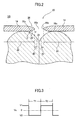
- FIG. 2 is an enlarged cross-sectional view showing essential portions of the electron emitter 10 of FIG. 1.
- the emitter section 12 is formed of a polycrystalline material. Therefore, as shown in FIGs. 1 and 2, microscopic concavities and convexities, which are attributed to grain boundaries, etc., are formed on the top surface 12a of the emitter section 12; specifically, concavities 24 are formed on the top surface 12a of the emitter section 12.
- the openings 20 of the first electrode 14 are formed in regions corresponding to the concavities 24. In the example illustrated in FIG. 1 or 2, the concavities 24 and the openings 20 are formed in one-to-one correspondence. However, in some cases, a single opening 20 may be formed for a plurality of concavities 24.
- each of the openings 20 includes a through hole 20a defined by the inner edge 26b of the opening 20, and a surrounding portion 26 (a portion of the first electrode 14) that surrounds the through hole 20a.
- the first electrode 14 is formed such that a surface 26a of the surrounding portion 26 of the opening 20 that faces the emitter section 12 is apart from the emitter section 12. In other words, a gap 28 is formed between the emitter section 12 and the surface 26a of the surrounding portion 26 of the opening 20, the surface 26a facing the emitter section 12.
- the cross section of the surrounding portion 26 of the opening 20 of the first electrode 14 assumes an overhanging form (flange form).
- the "surrounding portion 26 of the opening 20 of the first electrode 14" is called an "overhanging portion 26 of the first electrode 14."
- the "surface 26a of the surrounding portion 26 of the opening 20 of the first electrode 14 that faces the emitter section 12" is called a “lower surface 26a of the overhanging portion 26.”
- the top surface 12a of the emitter section 12 i.e., the surface in the vicinity of the vertexes of convexities
- the lower surface 26a of the overhanging portion 26 of the first electrode 14 form a maximum angle ⁇ that satisfies the following relation: 1° ⁇ ⁇ ⁇ 60°.
- the emitter section 12 and the first electrode 14 are formed such that the maximum gap d measured vertically between the top surface 12a of the emitter section 12 and the lower surface 26a of the overhanging portion 26 of the first electrode 14 is regulated so as to satisfy the following relation: 0 ⁇ m ⁇ d ⁇ 10 ⁇ m, and that the surface roughness Ra (centerline average roughness, unit: ⁇ m) of the top surface 12a is regulated to 0.005 or more and 0.5 or less.
- Triple junctions formed by contact among the first electrode 14, the emitter section 12, and a vacuum
- 26c are formed at contact sites among the top surface 12a of the emitter section 12, the first electrode 14, and a medium (e.g., a vacuum) surrounding the electron emitter 10.
- the triple junctions 26c are sites (electric field concentration points) at which lines of electric force concentrate (where electric field concentration occurs) when a drive voltage Va is applied between the first electrode 14 and the second electrode 16.
- the expression "site at which lines of electric force concentrate” refers to a site at which lines of electric force that are generated from the second electrode 16 at even intervals concentrate, when the lines of electric force are drawn under the assumption that the first electrode 14, the emitter section 12, and the second electrode 16 are flat plates each having a cross section extending infinitely.
- the state of the concentration of lines of electric force i.e., the state of electric field concentration
- the openings 20 are shaped such that the inner edges 26b thereof serve as the aforementioned electric field concentration points.
- the overhanging portion 26 of the opening 20 has such a cross-sectional shape as to be acutely pointed toward the inner edge 26b (the tip end of the overhanging portion 26); i.e., the thickness gradually decreases.
- the electric field concentration points, which are formed at the inner edge 26b of the opening 20 as described above, and the triple junctions 26c are also formed at sites corresponding to the peripheral edge portions 21 of the first electrode 14.
- the openings 20 may be formed to assume a variety of shapes as viewed in plane, including, a circular shape, an elliptical shape, a polygonal shape, and an irregular shape.
- the openings 20 are formed such that, when the through holes 20a as viewed in plane are approximated to circles having areas identical to those of the through holes 20a as viewed in plane, the average diameter of the circles (hereinafter may be referred to as "the average diameter of the through holes 20a”) becomes 0.1 ⁇ m or more and 20 ⁇ m or less. The reason for this is described below.
- regions of the emitter section 12 where polarization is inverted or changes in accordance with the drive voltage Va are regions (first regions) 40 located just under the first electrode 14, and regions (second regions) 42 corresponding to regions of the openings 20 that extend from the inner edges 26b (inner peripheries) of the openings 20 toward the centers of the openings 20.
- the range of the second region 42 varies depending on the level of the drive voltage Va and the degree of electric field concentration in the second region 42.
- the average diameter of the through holes 20a falls within the above-described range (i.e., 0.1 ⁇ m or more and 20 ⁇ m or less)
- electrons are efficiently emitted in a sufficient quantity through the openings 20.
- the area of the second regions 42 decreases.
- the second regions 42 form primary regions of the electron emission regions of the top surface 12a of the emitter section 12 for accumulating electrons supplied from the first electrode 14 to thereby contribute to electron emission. Therefore, a decrease in the area of the second regions 42 results in reduction of the quantity of electrons to be emitted.
- the ratio of the second regions 42 to regions of the emitter section 12 exposed through the openings 20 decreases, resulting in reduction of electron emission efficiency.
- the drive voltage Va to be applied between the first electrode 14 and the second electrode 16 is an alternating voltage of rectangular waveform having a period of T1 + T2.
- the reference voltage (voltage corresponding to the center of the wave) is 0 V; during time T1 corresponding to the first stage, the electric potential of the first electrode 14 is V2 (negative voltage), which is lower than the electric potential of the second electrode 16; and during time T2 corresponding to the second stage, the electric potential of the first electrode 14 is V1 (positive voltage), which is higher than the electric potential of the second electrode 16.
- the emitter section 12 In the initial state, the emitter section 12 is polarized unidirectionally. In the subsequent description, it is assumed that the emitter section 12 is initialized such that the negative poles of dipoles face toward the top surface 12a of the emitter section 12 (see FIG. 4A).
- the negative poles of dipoles face toward the top surface 12a of the emitter section 12, so that virtually no electrons are accumulated on the top surface 12a of the emitter section 12.
- This charging can be continued until a predetermined saturated condition, which depends on the surface resistance of the emitter section 12, is attained.
- the quantity of the charge can be controlled on the basis of application time of a control voltage.
- the first electrode 14 (particularly the aforementioned electric field concentration points) functions as an electron supply source for the emitter section 12 (top surface 12a).
- the structure of the electron emitter 10 can be approximated to a configuration in which a capacitor C1 associated with the emitter section 12 and an aggregate of a plurality of capacitors Ca associated with the gaps 28 are formed between the first electrode 14 and the second electrode 16.
- the equivalent circuit of the electron emitter can be formed as follows: the capacitors Ca associated with the gaps 28 are connected in parallel so as to act as a single capacitor C2, and the capacitor C2 is connected, in series, to the capacitor C1 associated with the emitter section 12.
- the equivalent circuit in which the capacitor C2 associated with the aforementioned aggregate is connected in series to the entirety of the capacitor C1 associated with the emitter section 12, is not practical. This is because, the percentage of the capacitor C1 to be connected in series to the capacitor C2 varies depending on, for example, the number of the openings 20 formed in the first electrode 14 and the overall area of the openings 20.
- the capacitor C2 which comprises the cluster of capacitors Ca has a capacitance of 0.885 pF, and the capacitor C1 due to the emitter section 12 has a capacitance of 35.4 pF. If the portion of the capacitor C1 due to the emitter section 12 which is connected in series to the capacitor C2 which comprises the cluster of capacitors Ca is 25% of the entire capacitor C1, then that series-connected portion has a capacitance (including the capacitance of capacitor C2 which comprises the cluster of capacitors Ca) of 0.805 pF, and the remaining portion has a capacitance of 26.6 pF.
- the overall capacitance between the first electrode 14 and the second electrode 16 is 27.5 pF, which is 78% of the capacitance of the capacitor C1 associated with the emitter section 12 (i.e., 35.4 pF). That is, the overall capacitance is lower than the capacitance of the capacitor C1 associated with the emitter section 12.
- the capacitance of the capacitors Ca associated with the gaps 28, or the overall capacitance of the capacitor C2 associated with the aggregate of the capacitors Ca is considerably lower than that of the capacitor C1 (associated with the emitter section 12) which is connected in series to the capacitor C2. Therefore, when the voltage Va is applied to the series circuit of the capacitors Ca (C2) and C1, most of the voltage Va is applied to the capacitors Ca (C2), whose capacitance is lower than that of the capacitor C1. In other words, most of the voltage Va is applied to the gaps 28. Therefore, the voltage is applied to the gaps 28 in a highly efficient manner, and thus a large number of electrons are emitted. That is, high emission of electrons is attained in the electron emitter.
- the capacitor C2 associated with the aggregate is connected, in series, to the capacitor C1 associated with the emitter section 12, the overall capacitance becomes lower than the capacitance of the capacitor C1 associated with the emitter section 12. This provides favorable characteristics of reduction in overall power consumption.
- the emitter section 12 employed in the first embodiment is formed from a dielectric composition containing, as a primary component, a composition represented by the following formula (1), and containing NiO in a predetermined amount.
- x, p, and z satisfy the following relations: 0.85 ⁇ x ⁇ 1.03, 0.02 ⁇ p ⁇ 0.1, and 0.8 ⁇ y ⁇ 1.0;
- a, b, and c are decimal numbers falling within a region formed by connecting the following five points (0.550, 0.425, 0.025), (0.550, 0.150, 0.300), (0.100, 0.150, 0.750), (0.100, 0.525, 0.375), and (0.375, 0.425, 0.200) in a triangular coordinate system of (a, b, c) having the following three vertexes (1, 0, 0), (0, 1, 1,
- the dielectric layer forming the emitter section 12 can be densified, and electron emission characteristics can be improved. Specifically, when the dielectric layer forming the emitter section 12 is densified, the number of defects in the dielectric layer is reduced, and therefore, during application of the drive voltage Va, the electric field intensity at the aforementioned gaps 28 is enhanced, resulting in an increase in the electron emission quantity. In addition, even when the electron emitter 10 is repeatedly used for a long period of time, deterioration of the electron emission performance of the emitter section 12 is improved; i.e., the electron emitter 10 exhibits enhanced durability.
- the dielectric layer is insufficiently densified, and the electron emission performance is deteriorated.
- the number of defects e.g., pores
- electric field concentration occurs at such defects, which have lower dielectric constant, whereby the electric field intensity decreases at the electron emission sites corresponding to the gaps 28, resulting in reduction of the electron emission quantity.
- the amount of Pb substituted by Bi is more preferably 2 to 5 mol%
- the amount of Ti substituted by Nb, etc. is more preferably 3 to 8 mol%
- the NiO content is more preferably 0.50 to 1.0 wt.%.
- a second electrode 16 containing Pt and having 1 mm X 0.5mm dimensions and a thickness of 3 ⁇ m is formed through screen printing.
- the substrate 11 having the thus-formed second electrode 16 is heated at about 1,000 to about 1,400°C, to thereby bond and combine the second electrode 16 with the substrate 11.
- the thickness of Pt after bond and combine is 1.5 ⁇ m
- a dielectric composition containing, as a primary component, a composition represented by formula (1) and containing NiO in a predetermined amount (mass%) is applied onto the second electrode 16 through screen printing, so as to form a thick layer having a dimension of 1.1 mm X 0.6mm and a thickness of 40 ⁇ m.
- Examples of the raw materials for the dielectric composition which may be employed include oxides of Pb, Mg, Nb, Zr, Ti, Ni, etc. (e.g., PbO, Pb 3 O 4 , MgO, Nb 2 O 5 , TiO 2 , ZrO 2 , and NiO etc.); carbonates of these elements; compounds containing two or more species of these elements (e.g., MgNb 2 O); these metallic elements per se ; and alloys of these elements. These raw materials may be employed singly or in combination of two or more species.
- the preparation method for the dielectric composition may be prepared through, for example, the following procedure.
- the aforementioned raw materials are mixed together such that the corresponding elements are contained in predetermined amounts by a general mixing machine such as a ball mill.
- the resultant raw material mixture is heated at 750 to 1,300°C, to thereby yield a dielectric composition.
- the ratio of the intensity of the strongest diffraction line of a phase other than a perovskite phase (e.g., a pyrochlore phase) to that of the strongest diffraction line of a perovskite phase is preferably 5% or less, more preferably 2% or less.
- the dielectric composition obtained through heating is milled by use of, for example, a ball mill, to thereby prepare dielectric composition powder particles having a predetermined particle size (e.g., an average particle size of 0.1 to 1 ⁇ m as measured by means of laser diffractometry).
- a predetermined particle size e.g., an average particle size of 0.1 to 1 ⁇ m as measured by means of laser diffractometry.
- arrangement of particle size may be performed by applying a heat treatment at 400 to 750°C to the dielectric composition obtained by milling. That is, the finer the particle size is, the easier the neighboring particles integrate during heating. Thus, integration of fine particles may progresses by above-mentioned heat treatment, and then the dielectric composition powder after heat treatment becomes even-sized powder. Therefore, the dielectric film which particle size is even-sized may be obtained.
- the thus-prepared dielectric composition powder particles are dispersed in a predetermined binder, to thereby prepare a paste.
- the paste is applied onto the second electrode 16 through screen printing as described above, to thereby form a thick layer.
- the thus-formed dielectric composition layer is heated, to thereby evaporate the binder and densify the dielectric layer. Through this procedure, the emitter section 12 is formed.
- a Pt-resinate-containing precursor is applied onto the above-formed emitter section 12 through screen printing at a dimension of 0.95mm X 0.45mm, followed by thermal treatment, to thereby form a first electrode (Pt electrode) 14.
- a first electrode Pt electrode
- Examples 1-1 through 1-8 and Comparative Examples 1-1 through 1-9 dielectric-film-type electron emitters were produced through the aforementioned production method.
- a display as shown in FIG. 1 was manufactured from the above-produced electron emitter, and the electron emitter was evaluated on the basis of the degree of reduction of brightness of the display after repeated use thereof. Specifically, the initial brightness of the display was measured; the display was subjected to durability testing (i.e., 10 9 cycles of electron emission operation); the brightness of the display after this durability testing (hereinafter may be referred to simply as "post-durability-test brightness") was measured; and the ratio of the post-durability-test brightness to the initial brightness (takes as 100%) was obtained.
- Each of the heated emitter sections 12 was found to have a thickness of 24 ⁇ m.
- Example 1-1 there was employed a dielectric composition containing, as a primary component, Pb 0.96 Bi 0.04 (Mg 1/3 Nb 2/3 ) 0.20 Ti 0.38 Nb 0.05 Zr 0.37 O 3 and containing NiO in an amount of 1.0 mass%.
- the post-durability-test brightness is 77%.
- the post-durability-test brightness is a half or less that in the case of Example 1-1.
- the post-durability-test brightness is about 60% or more.
- the post-durability-test brightness is less than 40%.
- the amount of Pb substituted by Bi falls within a range of 2 to 5 mol%
- the post-durability-test brightness is envisaged to become 70% or more.
- the Pb substitution amount is 2 to 4 mol%, very high post-durability-test brightness is attained.
- the post-durability-test brightness exceeds 60%.
- the post-durability-test brightness is less than 50%.
- the amount of Ti substituted by Nb falls within a range of 3 to 8 mol%
- the post-durability-test brightness is envisaged to become 70% or more.
- the Ti substitution amount is 5 to 8 mol%
- very high post-durability-test brightness is attained.
- the post-durability-test brightness is 55% or more.
- the post-durability-test brightness is less than 40%.
- the post-durability-test brightness is very high (about 70% or more).
- Example 1-9 1-10, or 1-11, the element corresponding to M in formula (1) was changed from Nb to Ta, Mo, or W, respectively.
- high post-durability-test brightness was attained.
- Table 5 Bi content (mol%) (Mg, Nb) content (mol%) Ti content (mol%) Zr content (mol%) Ti substitution element Ti substitution element content (mol%) NiO content (wt.%)
- Post -durability -test brightness Ex. 1-1 4 20 38 37 Nb 5 1.00 77% Ex. 1-9 4 20 38 37 Ta 5 1.00 71% Ex. 1-10 4 20 40 37 Mo 3 1.00 63% Ex.1-11 4 20 40 37 W 3 1.00 65%
- Example 1-1 which employs the dielectric composition containing, as a primary component, Pb 0.96 Bi 0.04 (Mg 1/3 Nb 2/3 ) 0.20 Ti 0.38 Nb 0.05 Zr 0.37 O 3 , and containing NiO in an amount of 1.0 mass%, or in the case where the amount of Pb substituted by Bi is 2 to 5 mol%, the amount of Ti substituted by Nb, etc. is 3 to 8 mol%, and the NiO content is 0.50 to 1.0 wt.%, the post-durability-test brightness becomes very high (70% or more), which is remarkably preferable.
- the emitted section 12 employed in the second embodiment is formed from a dielectric composition containing, as a primary component, a composition represented by formula (1), and containing NiO and MnO 2 in predetermined amounts. That is, the dielectric composition forming the emitter section 12 according to the second embodiment contains the dielectric composition employed in the first embodiment, and contains Mn (MnO 2 ) in a predetermined amount.
- the emitter section 12 and the electron emitter 10 including the emitter section 12 can be produced in a manner similar to that described above in the first embodiment.
- a display as shown in FIG. 1 was manufactured from the emitter section 12 according to the second embodiment, and the electron emitter 10 was evaluated on the basis of the degree of reduction of brightness of the display after repeated use.
- the electron emitters of Examples 1-12 through 1-14 which contain MnO 2 in different amounts, were compared with the electron emitter of Example 1-1, which contains no MnO 2 .
- the results are shown in Table 6.
- Table 6 Bi content (mol%) (Mg, Nb) content (mol%) Ti content (mol%) Zr content (mol%) Ti substitution element Ti substitution element content (mol%) NiO content (wt.%) MnO 2 content (wt.%) Post Post -durability -test brightness Ex.
- the post-durability-test brightness is high in the cases of Example 1-12 (MnO 2 content: 0.05 wt.%), Example 1-13 (MnO 2 content: 0.2 wt.%), and Example 1-14 (MnO 2 content: 1.0 wt.%).
- the post-durability-test brightness is very high (75% or more).
- the emitter section 12 employed in the third embodiment is formed from a dielectric composition containing, as a primary component, a composition represented by the following formula (2), and containing NiO in a predetermined amount (as in the cases of the aforementioned embodiments) (note: the dielectric composition is the aforementioned second dielectric composition).
- the dielectric composition forming the emitter section 12 according to the third embodiment is obtained by partially substituting Pb of the dielectric composition employed in the first embodiment by Sr in a predetermined amount.
- the emitter section 12 and the electron emitter 10 including the emitter section 12 can be produced in a manner similar to that of the above-described embodiments.
- the electron emitter was evaluated in a manner similar to that described above. The results are shown in Table 7.
- Post -durability -test brightness Ex. 1-1 4 0 20 38 37 Nb 5 1.00 77% Ex. 1-15 4 2 20 38 37 Nb 5 1.00 80% Ex. 1-16 4 10 20 38 37 Nb 5 1.00 79% Ex. 1-17 4 20 20 38 37 Nb 5 1.00 72%
- the post-durability-test brightness is high in the cases of Example 1-15 (amount of Pb substituted by Sr: 2 mol%), Example 1-16 (amount of Pb substituted by Sr: 10 mol%), and Example 1-17 (amount of Pb substituted by Sr: 20 mol%).
- the post-durability-test brightness is envisaged to become 75% or more.
- the post-durability-test brightness is very high (about 80%).
- the emitter section 12 employed in the fourth embodiment predominantly contains the aforementioned third dielectric composition; i.e., a dielectric composition represented by the following formula (3): Pb x (Mg y/3 Nb 2/3 ) a Ti b Z rc O 3 (3) [wherein x and y satisfy the following relations: 0.95 ⁇ x ⁇ 1.05 and 0.90 ⁇ y ⁇ 1.10; and a, b, and c are decimal numbers falling within a region formed by connecting the following five points (0.500, 0.350, 0.150), (0.500, 0.100, 0.400), (0.050, 0.100, 0.850), (0.050, 0.425, 0.525), and (0.250, 0.360, 0.390) in a triangular coordinate system of (a, b, c) having the following three vertexes (1, 0, 0), (0, 1, 0), and (0, 0, 1)].
- the dielectric composition represented by the aforementioned formula has, as a primary crystal phase, a rhombohedral crystal phase or a pseudocubic crystal phase, unlike the case of a conventional piezoelectric material formed of a lead-containing perovskite oxide having a tetragonal crystal phase as a primary crystal phase, such as a PZT material for a piezoelectric actuator or a ferroelectric memory.
- a second electrode 16 is formed on a substrate 11 formed of Y 2 O 3 -stabilized ZrO 2 through screen printing, and the second electrode 16 is bonded onto and combined with the substrate 11 through thermal treatment.
- a dielectric composition containing, as a primary component, a composition represented by formula (3) is applied onto the second electrode 16 through screen printing, so as to form a thick layer having a thickness of 40 ⁇ m. Thereafter, the thus-formed thick dielectric layer is heated together with the substrate 11, and is combined with the substrate 11, to thereby form the emitter section 12.
- the thermal treatment temperature is preferably 1,000 to 1,400°C, more preferably 1,100 to 1,350°C.
- the dielectric composition can be prepared in a manner similar to that described above in the first embodiment.
- the dielectric composition powder particles obtained through milling may be heated at 400 to 750°C for particle size regulation.
- a fine particle tends to aggregate with adjacent fine particles under heating. Therefore, when the dielectric composition powder particles (fine particles) are subjected to thermal treatment, aggregation of the fine particles proceeds, and the resultant dielectric powder particles exhibit a uniform particle size; i.e., the particles contained in the resultant dielectric layer exhibit a uniform particle size.
- a first electrode 14 is formed in a manner similar to that described above in the first embodiment.
- the piezoelectric-film-type electron emitter 10 of the fourth embodiment is produced.
- piezoelectric-film-type electron emitters were produced by use of dielectric compositions of Example 2 and Comparative Example 2 through the aforementioned production method.
- a display as shown in FIG. 1 was manufactured from the above-produced electron emitter, and the electron emitter was evaluated on the basis of the degree of reduction of brightness of the display after repeated use thereof.
- the initial brightness of the display was measured; the display was subjected to durability testing (i.e., 10 9 cycles of electron emission operation); the brightness of the display after this durability testing (post-durability-test brightness) was measured; and the ratio of the post-durability-test brightness to the initial brightness (taken as 100%) (the ratio will be called "durability" in the following description and tables) was obtained.
- durability testing i.e., 10 9 cycles of electron emission operation
- post-durability-test brightness was measured
- the ratio of the post-durability-test brightness to the initial brightness taken as 100%
- the ratio will be called "durability" in the following description and tables
- Examples 2-1 and 2-2 there were respectively employed a dielectric composition of formula (3) in which (a, b, c) are (0.375, 0.25, 0.375); and a dielectric composition of formula (3) in which (a, b, c) are (0.10, 0.36, 0.54).
- Comparative Examples 2-1, 2-2, and 2-3 there were respectively employed a dielectric composition of formula (3) in which (a, b, c) are (0.55, 0.175, 0.275); a dielectric composition of formula (3) in which (a, b, c) are (0.375, 0.050, 0.575); and a dielectric composition of formula (3) in which (a, b, c) are (0.03, 0.37, 0.60).
- Comparative Example 2-4 there was employed a dielectric composition represented by Pb(Mg 1/3 Nb 2/3 ) 0.20 Ti 0.38 Nb 0.05 Zr 0.37 O 3 (i.e., a dielectric composition in which Ti is partially substituted by Nb, and (a, b, c) are (0.20, 0.43, 0.37)).
- the evaluation results are shown in Table 8. In FIG.
- compositions corresponding to the Examples are represented by closed circles with suffixes (suffixes "1” and “2” correspond to Examples 2-1 and 2-2, respectively), and compositions corresponding to the Comparative Examples are represented by "*" with suffixes (suffixes "1,” “2,” “3,” and “4" correspond to Comparative Examples 2-1, 2-2, 2-3, and 2-4, respectively).
- Table 8 (Mg, Nb) content (mol%) Ti content (mol%) Zr content (mol%) Pb substitution element /element content (mol%) Ti substitution element /element content (mol%) Durability Ex. 2-1 37.5 25 37.5 - - 74% Ex. 2-2 10 36 54 - - 68% Comp. Ex. 2-1 55 17.5 27.5 - - 43% Comp. Ex. 2-2 37.5 5 57.5 - - 38% Comp. Ex. 2-3 3 37 60 - - 47% Comp. 20 38 37 - Nb/5 38%
- the durability is about 70%, whereas in the cases of Comparative Examples 2-1 through 2-3, the durability is less than 50%.
- a dielectric composition in which (a, b, c) fall within a region formed by connecting the following five points (0.500, 0.320, 0.180), (0.500, 0.100, 0.400), (0.050, 0.100, 0.850), (0.050, 0.425, 0.525), and (0.380, 0.320, 0.300) in the aforementioned triangular coordinate system; and more preferably, there is employed a dielectric composition in which (a, b, c) fall within a region formed by connecting the following six points (0.500, 0.320, 0.180), (0.500, 0.150, 0.350), (0.350, 0.150, 0.500), (0.050, 0.350, 0.600), (0-050, 0.425,
- a dielectric composition in which (a, b, c) fall within a region formed by connecting the following six points (0.500, 0.320, 0.180), (0.500, 0.150, 0.350), (0.350, 0.150, 0.500), (0.050, 0.350, 0.600), (0.050, 0.385, 0.565), and (0.380, 0.320, 0.300) in the triangular coordinate.
- the dielectric compositions employed in Example 2-1, Example 2-2, and Comparative Example 2-4 have, as a primary crystal phase, a pseudocubic crystal phase, a rhombohedral crystal phase, and a tetragonal crystal phase, respectively.
- the emitter section 12 employed in the fifth embodiment predominantly contains the aforementioned fourth dielectric composition; i.e., a dielectric composition represented by the following formula (4).
- This dielectric composition is obtained by substituting Pb of the third dielectric composition by another predetermined element.
- This dielectric composition is produced in a manner similar to that described in the fourth embodiment.
- piezoelectric-film-type electron emitters were produced by use of dielectric compositions of Examples 2-3 through 2-5, and the thus-produced electron emitters were subjected to evaluation.
- Examples 2-3, 2-4, and 2-5 there were respectively employed a dielectric composition of formula (4) in which (a, b, c) are (0.375, 0.25, 0.375), Ma is Sr, and p is 0.02; a dielectric composition of formula (4) in which (a, b, c) are (0.375, 0.25, 0.375), Ma is Sr, and p is 0.06; and a dielectric composition of formula (4) in which (a, b, c) are (0.375, 0.25, 0.375), Ma is Sr, and p is 0.12.
- the dielectric composition employed in each of Examples 2-3 through 2-5 is a dielectric composition obtained by substituting Pb of the dielectric composition (primary crystal phase: pseudocubic crystal phase) employed in Example 2-1 by Sr in a predetermined amount.
- the evaluation results of these Examples are shown in Table 9.
- the results of Example 2-1 are also shown in Table 9 for reference, since, as described above, the dielectric composition employed in Example 2-1 corresponds substantially to a dielectric composition of formula (4) in which p is zero.
- Table 9 (Mg, Nb) content (mol%) (mol % Ti content (mol%) (mol % Zr content (mol%) (mol % Pb substitution element /element content (mol%) Ti substitution element /element content (mol%) Durability Ex. 2-1 37.5 25 37.5 - - 74% Ex. 2-3 37.5 25 37.5 Sr/2 - 73% Ex. 2-4 37.5 25 37.5 Sr/6 - 76% Ex. 2-5 37.5 25 37.5 Sr/12 - 69%
- the results indicate that, when the value p (corresponding to the Sr content) falls within a range of 0.03 to 0.15, sufficient durability is envisaged to be attained, and that, from the viewpoint of attaining higher durability, the p value preferably falls within a range of 0.03 to 0.10, more preferably 0.05 to 0.07.
- Example 2-6, 2-7, and 2-8 there were respectively employed a dielectric composition of formula (4) in which Ma is La, and p is 0.002; a dielectric composition of formula (4) in which Ma is La, and p is 0.007; and a dielectric composition of formula (4) in which Ma is La, and p is 0.012.
- Example 2-9 there was employed a dielectric composition of formula (4) in which Ma is Bi, and p is 0.007.
- Table 10 Similar to the case of Table 9, the results of Example 2-1 (in which p is zero) are shown in Table 10 for reference.
- Example 2-9 As is clear from the results shown in Table 10, when p falls within a range of 0 to 0.012, a high durability of more than 70% is attained. No significant difference is observed in durability among the cases of Example 2-1 (in which p is zero), Example 2-6 (in which p is 0.002), and Example 2-8 (in which p is 0.012); i.e., no significant effect of La is observed in these Examples. In contrast, in the case of Example 2-7 (in which p is 0.007), the remarkable effect of La on durability improvement is observed. As is clear from the results of Example 2-9, the effect of Bi on durability improvement is observed.
- Example 2-10 there was employed a combination of the dielectric composition of Example 2-4 (i.e., a dielectric composition of formula (4) in which Ma is Sr, and p is 0.06), which exhibits the highest durability among the cases of Examples 2-3 through 2-5, and the dielectric composition of Example 2-7 (i.e., a dielectric composition of formula (4) in which Ma is La, and p is 0.007), which exhibits the highest durability among the cases of Examples 2-6 through 2-8.
- the evaluation results are shown in Table 11. Similar to the case of Table 9 or 10, the results of Example 2-1 (in which p is zero) are shown in Table 11 for reference.
- the emitter section 12 employed in the sixth embodiment predominantly contains the aforementioned fifth dielectric composition; i.e., a dielectric composition represented by the following formula (5).
- This dielectric composition is produced in a manner similar to that described in the fourth or fifth embodiment.
- piezoelectric-film-type electron emitters were produced in Examples 2-11 through 2-14, and the thus-produced electron emitters were subjected to evaluation.
- Examples 2-11, 2-12, 2-13, and 2-14 there were respectively employed a dielectric composition of formula (5) in which Mb is Nb, and q is 0.005; a dielectric composition of formula (5) in which Mb is Nb, and q is 0.02; a dielectric composition of formula (5) in which Mb is Nb, and q is 0.05; and a dielectric composition of formula (5) in which Mb is Nb, and q is 0.12.
- the dielectric composition employed in each of Examples 2-11 through 2-14 is a dielectric composition obtained by substituting Ti of the dielectric composition employed in Example 2-1 (in which (a, b, c) in formula (3) are (0.375, 0.25, 0.375)) by Nb in a predetermined amount.
- the evaluation results of these Examples are shown in Table 12.
- the results of Example 2-1 are also shown in Table 12 for reference, since the dielectric composition employed in Example 2-1 corresponds substantially to a dielectric composition of formula (5) in which q is zero.
- Table 12 (Mg, Nb) content (mol%) Ti content (mol%) Zr content (mol%) Pb substitution element /element content (mol%) Ti substitution element /element content (mol%) Durability Ex.
- the results indicate that, when the value q (corresponding to the Nb content) falls within a range of 0.01 to 0.15, sufficient durability is envisaged to be attained, and that, from the viewpoint of attaining higher durability, the q value preferably falls within a range of 0.02 to 0.10, more preferably 0.02 to 0.08.
- piezoelectric-film-type electron emitters were produced in Examples 2-15 through 2-17, and the thus-produced electron emitters were subjected to evaluation.
- dielectric compositions obtained through modification of the dielectric composition employed in Example 2-13 (i.e., a dielectric composition of formula (5) in which q is 0.05 and Mb is Nb), which exhibits the highest durability among the cases of Examples 2-11 through 2-14.
- dielectric compositions in which Mb is Ta a dielectric composition in which Mb is Mo
- Mb is W.
- Table 13 The evaluation results of these Examples are shown in Table 13.
- Example 2-1 In a manner similar to that described above, the results of Example 2-1 (in which q is zero) are shown in Table 13 for reference.
- Table 13 (Mg, Nb) content (mol%) Ti content content (mol%) Zr (mol%) Pb substitution element /element content (mol%) Ti substitution element /element content (mol%) Durability Ex. 2-1 37.5 25 37.5 - - 74% Ex. 2-15 37.5 25 37.5 - Ta/5 70% Ex. 2-16 37.5 25 37.5 - Mo/5 63% Ex. 2-17 37.5 25 37.5 - W/5 61%
- Example 2-10 which exhibits the highest durability among the cases of Examples 2-1 through 2-17
- the composition represented by the aforementioned PMN-PZ-PT ternary solid solution diagram is the same as that in the case of Example 2-1, and has a pseudocubic crystal phase as a primary crystal phase (i.e., the plot of Example 2-10 coincides with that of Example 2-1 in FIG. 8).
- Comparative Example 2-5 there was employed a dielectric composition obtained by modifying the dielectric composition of Example 2-10 so as to exhibit a tetragonal crystal phase, in which the mole fraction of PMN was not changed.
- the evaluation results are shown in Table 14.
- the results of Examples 2-1 and 2-2 are also shown in Table 14 for reference.
- Example 2-5 primary crystal phase: tetragonal crystal phase
- the electric-field-induced strain is as high as 0.098%, and the durability is considerably low.
- the electric-field-induced strain is 0.07% or less (i.e., 0.06% for Example 2-1, 0.056% for Example 2-2, and 0.065% for Example 2-10).
- the durability is about 70%.
- Example 2-1, 2-2, or 2-10 primary crystal phase: pseudocubic or rhombohedral crystal phase
- Examples of the raw materials which may be employed for the aforementioned dielectric compositions include oxides of Pb, Mg, Nb, Zr, Ti, Ni, etc. (e.g., PbO, Pb 3 O 4 , MgO, Nb 2 O 5 , TiO 2 , and ZrO 2 etc.); carbonates of these elements; compounds containing two or more species of these elements (e.g., MgNb 2 O) these metallic elements per se; and alloys of these elements. These raw materials may be employed singly or in combination of two or more species.
- Addition of Ni may be performed through any technique, so long as the Ni content (as reduced to NiO) falls within the aforementioned range.
- NiO is added to a dielectric composition which has been prepared in advance.
- the thus-added Ni (NiO) is uniformly dispersed in the emitter section 12.
- the Ni (NiO) may be dispersed in the emitter section 12 such that the Ni (NiO) concentration increases in a thickness direction of the emitter section 12 from the bottom surface 12b (which is bonded onto the substrate 11) toward the top surface 12a.
- the dielectric composition forming the emitter section 12 may be prepared through a variety of techniques other than the technique described above in the Examples.
- the dielectric composition may be prepared through the alkoxide method or the coprecipitation method.
- thermal treatment is preferably performed after formation of the first electrode 14 or the second electrode 16, the thermal treatment is not necessarily carried out.
- thermal treatment is performed after the second electrode 16 is formed on the substrate 11 as described above the Examples.
- the configuration of the electron emitter of the present invention is not limited to that of the electron emitter described above in the embodiments.
- both the first electrode 14 and the second electrode 16 may be formed on the top surface 12a of the electron emitter 12, although, in the aforementioned embodiments, the first electrode 14 and the second electrode 16 are respectively formed on the top surface 12a and the bottom surface 12b of the emitter section 12.
- Each of the first electrode 14, the emitter section 12, and the second electrode 16 may have a multi-layer structure.
- the substrate 11 may be formed of a glass or metallic material in place of a ceramic material. No particular limitation is imposed on the type of the ceramic material to be employed. However, from the viewpoints of heat resistance, chemical stability, and insulating property, the substrate 11 is preferably formed of a ceramic material containing at least one species selected from the group consisting of stabilized zirconium oxide, aluminum oxide, magnesium oxide, mullite, aluminum nitride, silicon nitride, and glass. More preferably, the substrate 11 is formed of stabilized zirconium oxide, from the viewpoints of high mechanical strength and excellent toughness.
- the term "stabilized zirconium oxide” refers to zirconium oxide in which crystal phase transition is improved through addition of a stabilizer.
- the stabilized zirconium oxide encompasses partially stabilized zirconium oxide.
- Examples of the stabilized zirconium oxide include zirconium oxide containing a stabilizer (e.g., calcium oxide, magnesium oxide, yttrium oxide, scandium oxide, ytterbium oxide, cerium oxide, or an oxide of a rare earth metal) in an amount of 1 to 30 mol%. From the viewpoint of further enhancement of the mechanical strength of a vibration section, zirconium oxide containing yttrium oxide as a stabilizer is preferably employed.
- the yttrium oxide content is preferably 1.5 to 6 mol%, more preferably 2 to 4 mol%.
- Zirconium oxide containing, in addition to yttrium oxide, aluminum oxide in an amount of 0.1 to 5 mol% is more preferred.
- Titanium oxide is contained in an amount of 0.1 to 10 mol%.
- the stabilized zirconium oxide may have, for example, a cubic-monoclinic mixed crystal phase, a tetragonal-monoclinic mixed crystal phase, or a cubic-tetragonal-monoclinic mixed crystal phase.
- the stabilized zirconium oxide preferably has, as a primary crystal phase, a tetragonal crystal phase or a tetragonal-cubic mixed crystal phase.
- Pb may be partially substituted by two or more elements selected from among Sr, La, and Bi (similarly, Ti may be partially substituted by two or more elements selected from among Nb, Ta, Mo, and W).
- Ti may be partially substituted by two or more elements selected from among Nb, Ta, Mo, and W.
- dielectric composition in which Pb is partially substituted by Sr, La, or Bi, and Ti is partially substituted by Nb, Ta, Mo, or W (this dielectric composition corresponds to the aforementioned sixth dielectric composition).
- the first electrode 14 or the second electrode 16 may be formed of an electrically conductive material (e.g., metallic particles, metallic film, or electrically conductive non-metallic film) other than electrically conductive non-metallic particles.
- the metal which may be employed include at least one metal selected from the group consisting of platinum, palladium, rhodium, gold, silver, and an alloy thereof.
- platinum or an alloy predominantly containing platinum is preferably employed.
- a silver-palladium alloy is preferably employed.
- the openings 20 of the first electrode 14 may assume a variety of shapes other than the shapes described above in the embodiments.
- the overhanging portion 26 corresponding to each of the openings 20, at which lines of electric force concentrate may have a cross-sectional shape such that the thickness of the first electrode 14 gradually decreases toward the inner edge 26b; for example, a cross-sectional shape as shown in FIG. 2, in which the overhanging portion 26 is acutely pointed toward the center (in a thickness direction) of the first electrode 14, or a cross-sectional shape in which the overhanging portion 26 is acutely pointed toward the bottom surface of the first electrode 14.
- the aforementioned shape of the opening 20 may be attained by providing a projection having a sharp cross section to the inner wall of the opening, or by depositing electrically conductive fine particles onto the inner wall thereof.
- the aforementioned shape of the opening 20 may be attained by imparting a hyperboloidal profile (particularly a hyperboloidal profile such that the cross section of the opening 20 has a sharp upper end and a sharp lower end at the inner edge of the opening 20) to the inner wall of the opening 20.
- Examples of the technique for forming the electrodes include the ion beam method, sputtering, vacuum evaporation, PVD, ion plating, CVD, plating, screen printing, spraying, and dipping. Of these, from the viewpoint of strong joint between the substrate and the dielectric layer, screen printing or sputtering is preferably employed.
Landscapes
- Chemical & Material Sciences (AREA)
- Engineering & Computer Science (AREA)
- Ceramic Engineering (AREA)
- Nanotechnology (AREA)
- Manufacturing & Machinery (AREA)
- Crystallography & Structural Chemistry (AREA)
- Theoretical Computer Science (AREA)
- Composite Materials (AREA)
- Physics & Mathematics (AREA)
- Mathematical Physics (AREA)
- Materials Engineering (AREA)
- Structural Engineering (AREA)
- Organic Chemistry (AREA)
- Cold Cathode And The Manufacture (AREA)
- Compositions Of Oxide Ceramics (AREA)
- Inorganic Insulating Materials (AREA)
Applications Claiming Priority (3)
| Application Number | Priority Date | Filing Date | Title |
|---|---|---|---|
| JP2004245833 | 2004-08-25 | ||
| JP2004274905 | 2004-09-22 | ||
| JP2005208337A JP4827451B2 (ja) | 2004-08-25 | 2005-07-19 | 電子放出素子 |
Publications (3)
| Publication Number | Publication Date |
|---|---|
| EP1630842A2 true EP1630842A2 (de) | 2006-03-01 |
| EP1630842A3 EP1630842A3 (de) | 2008-05-28 |
| EP1630842B1 EP1630842B1 (de) | 2009-07-29 |
Family
ID=35106806
Family Applications (1)
| Application Number | Title | Priority Date | Filing Date |
|---|---|---|---|
| EP20050255199 Expired - Lifetime EP1630842B1 (de) | 2004-08-25 | 2005-08-24 | Elektronenemitter |
Country Status (3)
| Country | Link |
|---|---|
| EP (1) | EP1630842B1 (de) |
| JP (1) | JP4827451B2 (de) |
| DE (1) | DE602005015654D1 (de) |
Families Citing this family (1)
| Publication number | Priority date | Publication date | Assignee | Title |
|---|---|---|---|---|
| JP4884115B2 (ja) * | 2006-07-20 | 2012-02-29 | 日本碍子株式会社 | 電子放出素子 |
Citations (2)
| Publication number | Priority date | Publication date | Assignee | Title |
|---|---|---|---|---|
| JP2004146365A (ja) | 2002-09-30 | 2004-05-20 | Ngk Insulators Ltd | 発光装置 |
| JP2004172087A (ja) | 2002-11-05 | 2004-06-17 | Ngk Insulators Ltd | ディスプレイ |
Family Cites Families (13)
| Publication number | Priority date | Publication date | Assignee | Title |
|---|---|---|---|---|
| JPS6144764A (ja) * | 1984-08-07 | 1986-03-04 | 宇部興産株式会社 | アクチュエータ |
| DE68918473T2 (de) * | 1988-03-04 | 1995-02-09 | Hitachi Ltd | Funktionaler keramischer Formkörper und Verfahren zu seiner Herstellung. |
| JPH08198672A (ja) * | 1995-01-18 | 1996-08-06 | Toyota Central Res & Dev Lab Inc | 圧電材料 |
| JPH08264104A (ja) * | 1995-03-27 | 1996-10-11 | Kanebo Ltd | 強誘電体電子放出冷陰極 |
| JPH0945226A (ja) * | 1995-07-31 | 1997-02-14 | Canon Inc | 電子放出素子、それを用いた電子源並びに画像形成装置と、それらの製造方法 |
| JPH10139594A (ja) * | 1996-10-30 | 1998-05-26 | Seiko Epson Corp | 圧電体薄膜およびその製造法ならびにそれを用いたインクジェット記録ヘッド |
| JPH10139540A (ja) * | 1996-10-31 | 1998-05-26 | Toyota Central Res & Dev Lab Inc | 圧電材料 |
| GB9702348D0 (en) * | 1997-02-05 | 1997-03-26 | Smiths Industries Plc | Electron emitter devices |
| JPH11163273A (ja) * | 1997-12-01 | 1999-06-18 | Tokyo Ohka Kogyo Co Ltd | 誘電体薄膜、誘電体キャパシタの製造方法、および誘電体メモリ |
| JP4141591B2 (ja) * | 1999-07-06 | 2008-08-27 | 株式会社日立製作所 | 表示装置の製造方法 |
| EP1265263A4 (de) * | 2000-12-22 | 2006-11-08 | Ngk Insulators Ltd | Elektronenemissionselement und dieses verwen-dende feldemissionsanzeige |
| CN1216394C (zh) * | 2001-09-25 | 2005-08-24 | 松下电工株式会社 | 场致发射型电子源 |
| JP3869819B2 (ja) * | 2002-11-29 | 2007-01-17 | 日本碍子株式会社 | 電子放出素子 |
-
2005
- 2005-07-19 JP JP2005208337A patent/JP4827451B2/ja not_active Expired - Fee Related
- 2005-08-24 DE DE200560015654 patent/DE602005015654D1/de not_active Expired - Lifetime
- 2005-08-24 EP EP20050255199 patent/EP1630842B1/de not_active Expired - Lifetime
Patent Citations (2)
| Publication number | Priority date | Publication date | Assignee | Title |
|---|---|---|---|---|
| JP2004146365A (ja) | 2002-09-30 | 2004-05-20 | Ngk Insulators Ltd | 発光装置 |
| JP2004172087A (ja) | 2002-11-05 | 2004-06-17 | Ngk Insulators Ltd | ディスプレイ |
Also Published As
| Publication number | Publication date |
|---|---|
| DE602005015654D1 (de) | 2009-09-10 |
| JP2006120611A (ja) | 2006-05-11 |
| EP1630842A3 (de) | 2008-05-28 |
| EP1630842B1 (de) | 2009-07-29 |
| JP4827451B2 (ja) | 2011-11-30 |
Similar Documents
| Publication | Publication Date | Title |
|---|---|---|
| US7842398B2 (en) | Dielectric device | |
| US7088049B2 (en) | Electron-emitting device and field emission display using the same | |
| US20040090398A1 (en) | Display | |
| US7723909B2 (en) | Electron emitter formed of a dielectric material characterized by having high mechanical quality factor | |
| EP1617449A2 (de) | Dielektrische Vorrichtung | |
| JP2005116232A (ja) | 電子放出素子及びその製造方法 | |
| EP2131409B1 (de) | Laminierter piezoelektrischer aktor und flüssigkeitsausspritzkopf | |
| US7511409B2 (en) | Dielectric film element and composition | |
| JP2004228065A (ja) | 電子パルス放出装置 | |
| US10388851B2 (en) | Piezoelectric element | |
| EP1630842B1 (de) | Elektronenemitter | |
| US7276462B2 (en) | Dielectric composition and dielectric film element | |
| US6936972B2 (en) | Electron-emitting element and field emission display using the same | |
| EP1637508A2 (de) | Dielektrische Zusammensetzung und dielektrisches Filmelement | |
| US20080048569A1 (en) | Dielectric element and electron emitter | |
| US7576479B2 (en) | Electron emitter | |
| JP3848237B2 (ja) | 電子放出素子及びそれを用いたフィールドエミッションディスプレイ | |
| US7727585B2 (en) | Dielectric device and its manufacturing method | |
| US7727584B2 (en) | Dielectric device and its manufacturing method | |
| CN100400465C (zh) | 电介质组成物及电介质膜元件 | |
| US20030038600A1 (en) | Electron-emitting device and field emission display using the same | |
| EP1617451A2 (de) | Dielektrische Vorrichtung | |
| JP2005044918A (ja) | 圧電/電歪素子の製造方法 |
Legal Events
| Date | Code | Title | Description |
|---|---|---|---|
| PUAI | Public reference made under article 153(3) epc to a published international application that has entered the european phase |
Free format text: ORIGINAL CODE: 0009012 |
|
| 17P | Request for examination filed |
Effective date: 20050913 |
|
| AK | Designated contracting states |
Kind code of ref document: A2 Designated state(s): AT BE BG CH CY CZ DE DK EE ES FI FR GB GR HU IE IS IT LI LT LU LV MC NL PL PT RO SE SI SK TR |
|
| AX | Request for extension of the european patent |
Extension state: AL BA HR MK YU |
|
| PUAL | Search report despatched |
Free format text: ORIGINAL CODE: 0009013 |
|
| AK | Designated contracting states |
Kind code of ref document: A3 Designated state(s): AT BE BG CH CY CZ DE DK EE ES FI FR GB GR HU IE IS IT LI LT LU LV MC NL PL PT RO SE SI SK TR |
|
| AX | Request for extension of the european patent |
Extension state: AL BA HR MK YU |
|
| GRAP | Despatch of communication of intention to grant a patent |
Free format text: ORIGINAL CODE: EPIDOSNIGR1 |
|
| AKX | Designation fees paid |
Designated state(s): DE FR GB |
|
| RIC1 | Information provided on ipc code assigned before grant |
Ipc: H01J 1/312 20060101AFI20090113BHEP |
|
| GRAS | Grant fee paid |
Free format text: ORIGINAL CODE: EPIDOSNIGR3 |
|
| GRAA | (expected) grant |
Free format text: ORIGINAL CODE: 0009210 |
|
| AK | Designated contracting states |
Kind code of ref document: B1 Designated state(s): DE FR GB |
|
| REG | Reference to a national code |
Ref country code: GB Ref legal event code: FG4D |
|
| REF | Corresponds to: |
Ref document number: 602005015654 Country of ref document: DE Date of ref document: 20090910 Kind code of ref document: P |
|
| PLBE | No opposition filed within time limit |
Free format text: ORIGINAL CODE: 0009261 |
|
| STAA | Information on the status of an ep patent application or granted ep patent |
Free format text: STATUS: NO OPPOSITION FILED WITHIN TIME LIMIT |
|
| 26N | No opposition filed |
Effective date: 20100503 |
|
| PGFP | Annual fee paid to national office [announced via postgrant information from national office to epo] |
Ref country code: GB Payment date: 20120726 Year of fee payment: 8 |
|
| PGFP | Annual fee paid to national office [announced via postgrant information from national office to epo] |
Ref country code: FR Payment date: 20120809 Year of fee payment: 8 |
|
| GBPC | Gb: european patent ceased through non-payment of renewal fee |
Effective date: 20130824 |
|
| REG | Reference to a national code |
Ref country code: FR Ref legal event code: ST Effective date: 20140430 |
|
| PG25 | Lapsed in a contracting state [announced via postgrant information from national office to epo] |
Ref country code: GB Free format text: LAPSE BECAUSE OF NON-PAYMENT OF DUE FEES Effective date: 20130824 |
|
| PG25 | Lapsed in a contracting state [announced via postgrant information from national office to epo] |
Ref country code: FR Free format text: LAPSE BECAUSE OF NON-PAYMENT OF DUE FEES Effective date: 20130902 |
|
| PGFP | Annual fee paid to national office [announced via postgrant information from national office to epo] |
Ref country code: DE Payment date: 20160816 Year of fee payment: 12 |
|
| REG | Reference to a national code |
Ref country code: DE Ref legal event code: R119 Ref document number: 602005015654 Country of ref document: DE |
|
| PG25 | Lapsed in a contracting state [announced via postgrant information from national office to epo] |
Ref country code: DE Free format text: LAPSE BECAUSE OF NON-PAYMENT OF DUE FEES Effective date: 20180301 |