EP1630867A2 - Procédé pour la fabrication d'un dispositif semi-conducteur et dispositif semi-conducteur - Google Patents
Procédé pour la fabrication d'un dispositif semi-conducteur et dispositif semi-conducteur Download PDFInfo
- Publication number
- EP1630867A2 EP1630867A2 EP05016769A EP05016769A EP1630867A2 EP 1630867 A2 EP1630867 A2 EP 1630867A2 EP 05016769 A EP05016769 A EP 05016769A EP 05016769 A EP05016769 A EP 05016769A EP 1630867 A2 EP1630867 A2 EP 1630867A2
- Authority
- EP
- European Patent Office
- Prior art keywords
- semiconductor chip
- terminal
- surface side
- semiconductor
- substrate
- Prior art date
- Legal status (The legal status is an assumption and is not a legal conclusion. Google has not performed a legal analysis and makes no representation as to the accuracy of the status listed.)
- Withdrawn
Links
Images

Classifications
-
- H—ELECTRICITY
- H10—SEMICONDUCTOR DEVICES; ELECTRIC SOLID-STATE DEVICES NOT OTHERWISE PROVIDED FOR
- H10W—GENERIC PACKAGES, INTERCONNECTIONS, CONNECTORS OR OTHER CONSTRUCTIONAL DETAILS OF DEVICES COVERED BY CLASS H10
- H10W90/00—Package configurations
-
- H—ELECTRICITY
- H10—SEMICONDUCTOR DEVICES; ELECTRIC SOLID-STATE DEVICES NOT OTHERWISE PROVIDED FOR
- H10W—GENERIC PACKAGES, INTERCONNECTIONS, CONNECTORS OR OTHER CONSTRUCTIONAL DETAILS OF DEVICES COVERED BY CLASS H10
- H10W70/00—Package substrates; Interposers; Redistribution layers [RDL]
- H10W70/60—Insulating or insulated package substrates; Interposers; Redistribution layers
-
- H—ELECTRICITY
- H10—SEMICONDUCTOR DEVICES; ELECTRIC SOLID-STATE DEVICES NOT OTHERWISE PROVIDED FOR
- H10W—GENERIC PACKAGES, INTERCONNECTIONS, CONNECTORS OR OTHER CONSTRUCTIONAL DETAILS OF DEVICES COVERED BY CLASS H10
- H10W20/00—Interconnections in chips, wafers or substrates
- H10W20/01—Manufacture or treatment
- H10W20/021—Manufacture or treatment of interconnections within wafers or substrates
- H10W20/023—Manufacture or treatment of interconnections within wafers or substrates the interconnections being through-semiconductor vias
- H10W20/0238—Manufacture or treatment of interconnections within wafers or substrates the interconnections being through-semiconductor vias comprising etching via holes through pads or through electrodes
-
- H—ELECTRICITY
- H10—SEMICONDUCTOR DEVICES; ELECTRIC SOLID-STATE DEVICES NOT OTHERWISE PROVIDED FOR
- H10W—GENERIC PACKAGES, INTERCONNECTIONS, CONNECTORS OR OTHER CONSTRUCTIONAL DETAILS OF DEVICES COVERED BY CLASS H10
- H10W20/00—Interconnections in chips, wafers or substrates
- H10W20/01—Manufacture or treatment
- H10W20/021—Manufacture or treatment of interconnections within wafers or substrates
- H10W20/023—Manufacture or treatment of interconnections within wafers or substrates the interconnections being through-semiconductor vias
- H10W20/0249—Manufacture or treatment of interconnections within wafers or substrates the interconnections being through-semiconductor vias wherein the through-semiconductor via protrudes from backsides of the chips, wafers or substrates during the manufacture
-
- H—ELECTRICITY
- H10—SEMICONDUCTOR DEVICES; ELECTRIC SOLID-STATE DEVICES NOT OTHERWISE PROVIDED FOR
- H10W—GENERIC PACKAGES, INTERCONNECTIONS, CONNECTORS OR OTHER CONSTRUCTIONAL DETAILS OF DEVICES COVERED BY CLASS H10
- H10W20/00—Interconnections in chips, wafers or substrates
- H10W20/20—Interconnections within wafers or substrates, e.g. through-silicon vias [TSV]
-
- H—ELECTRICITY
- H10—SEMICONDUCTOR DEVICES; ELECTRIC SOLID-STATE DEVICES NOT OTHERWISE PROVIDED FOR
- H10W—GENERIC PACKAGES, INTERCONNECTIONS, CONNECTORS OR OTHER CONSTRUCTIONAL DETAILS OF DEVICES COVERED BY CLASS H10
- H10W72/00—Interconnections or connectors in packages
- H10W72/20—Bump connectors, e.g. solder bumps or copper pillars; Dummy bumps; Thermal bumps
- H10W72/221—Structures or relative sizes
-
- H—ELECTRICITY
- H10—SEMICONDUCTOR DEVICES; ELECTRIC SOLID-STATE DEVICES NOT OTHERWISE PROVIDED FOR
- H10W—GENERIC PACKAGES, INTERCONNECTIONS, CONNECTORS OR OTHER CONSTRUCTIONAL DETAILS OF DEVICES COVERED BY CLASS H10
- H10W72/00—Interconnections or connectors in packages
- H10W72/20—Bump connectors, e.g. solder bumps or copper pillars; Dummy bumps; Thermal bumps
- H10W72/221—Structures or relative sizes
- H10W72/222—Multilayered bumps, e.g. a coating on top and side surfaces of a bump core
-
- H—ELECTRICITY
- H10—SEMICONDUCTOR DEVICES; ELECTRIC SOLID-STATE DEVICES NOT OTHERWISE PROVIDED FOR
- H10W—GENERIC PACKAGES, INTERCONNECTIONS, CONNECTORS OR OTHER CONSTRUCTIONAL DETAILS OF DEVICES COVERED BY CLASS H10
- H10W72/00—Interconnections or connectors in packages
- H10W72/20—Bump connectors, e.g. solder bumps or copper pillars; Dummy bumps; Thermal bumps
- H10W72/241—Dispositions, e.g. layouts
- H10W72/244—Dispositions, e.g. layouts relative to underlying supporting features, e.g. bond pads, RDLs or vias
-
- H—ELECTRICITY
- H10—SEMICONDUCTOR DEVICES; ELECTRIC SOLID-STATE DEVICES NOT OTHERWISE PROVIDED FOR
- H10W—GENERIC PACKAGES, INTERCONNECTIONS, CONNECTORS OR OTHER CONSTRUCTIONAL DETAILS OF DEVICES COVERED BY CLASS H10
- H10W72/00—Interconnections or connectors in packages
- H10W72/20—Bump connectors, e.g. solder bumps or copper pillars; Dummy bumps; Thermal bumps
- H10W72/251—Materials
- H10W72/252—Materials comprising solid metals or solid metalloids, e.g. PbSn, Ag or Cu
-
- H—ELECTRICITY
- H10—SEMICONDUCTOR DEVICES; ELECTRIC SOLID-STATE DEVICES NOT OTHERWISE PROVIDED FOR
- H10W—GENERIC PACKAGES, INTERCONNECTIONS, CONNECTORS OR OTHER CONSTRUCTIONAL DETAILS OF DEVICES COVERED BY CLASS H10
- H10W72/00—Interconnections or connectors in packages
- H10W72/90—Bond pads, in general
- H10W72/921—Structures or relative sizes of bond pads
- H10W72/922—Bond pads being integral with underlying chip-level interconnections
- H10W72/9226—Bond pads being integral with underlying chip-level interconnections with via interconnections
-
- H—ELECTRICITY
- H10—SEMICONDUCTOR DEVICES; ELECTRIC SOLID-STATE DEVICES NOT OTHERWISE PROVIDED FOR
- H10W—GENERIC PACKAGES, INTERCONNECTIONS, CONNECTORS OR OTHER CONSTRUCTIONAL DETAILS OF DEVICES COVERED BY CLASS H10
- H10W72/00—Interconnections or connectors in packages
- H10W72/90—Bond pads, in general
- H10W72/921—Structures or relative sizes of bond pads
- H10W72/923—Bond pads having multiple stacked layers
-
- H—ELECTRICITY
- H10—SEMICONDUCTOR DEVICES; ELECTRIC SOLID-STATE DEVICES NOT OTHERWISE PROVIDED FOR
- H10W—GENERIC PACKAGES, INTERCONNECTIONS, CONNECTORS OR OTHER CONSTRUCTIONAL DETAILS OF DEVICES COVERED BY CLASS H10
- H10W72/00—Interconnections or connectors in packages
- H10W72/90—Bond pads, in general
- H10W72/941—Dispositions of bond pads
- H10W72/942—Dispositions of bond pads relative to underlying supporting features, e.g. bond pads, RDLs or vias
-
- H—ELECTRICITY
- H10—SEMICONDUCTOR DEVICES; ELECTRIC SOLID-STATE DEVICES NOT OTHERWISE PROVIDED FOR
- H10W—GENERIC PACKAGES, INTERCONNECTIONS, CONNECTORS OR OTHER CONSTRUCTIONAL DETAILS OF DEVICES COVERED BY CLASS H10
- H10W72/00—Interconnections or connectors in packages
- H10W72/90—Bond pads, in general
- H10W72/951—Materials of bond pads
- H10W72/952—Materials of bond pads comprising metals or metalloids, e.g. PbSn, Ag or Cu
-
- H—ELECTRICITY
- H10—SEMICONDUCTOR DEVICES; ELECTRIC SOLID-STATE DEVICES NOT OTHERWISE PROVIDED FOR
- H10W—GENERIC PACKAGES, INTERCONNECTIONS, CONNECTORS OR OTHER CONSTRUCTIONAL DETAILS OF DEVICES COVERED BY CLASS H10
- H10W90/00—Package configurations
- H10W90/20—Configurations of stacked chips
- H10W90/291—Configurations of stacked chips characterised by containers, encapsulations, or other housings for the stacked chips
-
- H—ELECTRICITY
- H10—SEMICONDUCTOR DEVICES; ELECTRIC SOLID-STATE DEVICES NOT OTHERWISE PROVIDED FOR
- H10W—GENERIC PACKAGES, INTERCONNECTIONS, CONNECTORS OR OTHER CONSTRUCTIONAL DETAILS OF DEVICES COVERED BY CLASS H10
- H10W90/00—Package configurations
- H10W90/20—Configurations of stacked chips
- H10W90/297—Configurations of stacked chips characterised by the through-semiconductor vias [TSVs] in the stacked chips
-
- H—ELECTRICITY
- H10—SEMICONDUCTOR DEVICES; ELECTRIC SOLID-STATE DEVICES NOT OTHERWISE PROVIDED FOR
- H10W—GENERIC PACKAGES, INTERCONNECTIONS, CONNECTORS OR OTHER CONSTRUCTIONAL DETAILS OF DEVICES COVERED BY CLASS H10
- H10W90/00—Package configurations
- H10W90/701—Package configurations characterised by the relative positions of pads or connectors relative to package parts
- H10W90/721—Package configurations characterised by the relative positions of pads or connectors relative to package parts of bump connectors
- H10W90/722—Package configurations characterised by the relative positions of pads or connectors relative to package parts of bump connectors between stacked chips
Definitions
- the present invention relates to a method for manufacturing a semiconductor device, and to a semiconductor device.
- a method is known in which semiconductor chips that are provided with trans-substrate conductive plugs that are located on top of a chip substrate and terminals that are connected to these trans-substrate conductive plugs are stacked after a connection surface of the terminals has undergone activation processing (see, for example, Japanese Unexamined Patent Application, First Publication No. 2002-170919).
- the semiconductor chips because the semiconductor chips are constructed with the trans-substrate conductive plugs and the terminals being formed separately on top of the semiconductor chips, the semiconductor chips end up having a considerable size and it has been difficult to efficiently increase the packaging density.
- the active surface side i.e., the surface on which an integrated circuit is formed
- the size of the outer shape of the trans-substrate conductive plug that protrudes on the back surface side of the semiconductor chip are formed at different sizes (for example, see Japanese Unexamined Patent Application, First Publication No. 2003-282819.
- the terminal on the active surface side is made larger than the terminal on the back surface side. Accordingly, when semiconductor chips are being stacked, by placing a large terminal in contact with a small terminal it becomes easy to align terminals of adjacent semiconductor chips.
- solder i.e., a brazing material
- solder layer has been formed on the trans-substrate conductive plug terminal that has a large outer shape and protrudes from the active surface side.
- the brazing material is connected to both the second terminal and the connecting electrode via the alloy layer, the second terminal and the connecting electrode are reliably bonded resulting in an excellent bond being obtained.
- the connecting body may be another semiconductor chip having the same structure as the semiconductor chip, and the brazing material may be provided on a first terminal of the another semiconductor chip that serves as the connecting body, and the method may further include placing the first terminal of the another semiconductor chip and the second terminal of the semiconductor chip that is stacked on top of the another semiconductor chip against each other; and electrically connecting the first terminal of the another semiconductor chip and the second terminal of the semiconductor chip via the brazing material.
- a semiconductor chip on which a redistribution layer has been formed by W-CSP (wafer level chip scale package) processing on, for example, the first terminal side thereof is stacked on the semiconductor chip that serves as a connecting body.
- W-CSP wafer level chip scale package
- the applied heat is conducted first from the second terminal of the semiconductor chip that has undergone W-CSP processing to the brazing material that is provided on the first terminal of the semiconductor chip that serves as a connecting body, so that an alloy layer is formed at the interfaces between the second terminal surface and the brazing material.
- this stacked body is inverted.
- the method may further include: placing the first terminal of the semiconductor chip and a second terminal of the second semiconductor chip that is stacked on top of the semiconductor chip against each other, and electrically connecting the first terminal of the semiconductor chip and the second terminal of the second semiconductor chip via the brazing material.
- the brazing material forms an alloy layer at interfaces between the second terminal and the brazing material.
- the interface between the first terminal and the brazing material form an alloy layer from the time when the brazing material is first formed. Accordingly, the second terminal and the first terminal can be securely bonded via the brazing material that has been formed into an alloy layer. Accordingly, an excellent bond is obtained using brazing material and a semiconductor device in which the semiconductor chips are securely stacked can be manufactured.
- the brazing material is melted at the time when the semiconductor chip is stacked, the brazing material is not affected by gravity as it is supported by the first terminal. Accordingly, it is possible to prevent short-circuiting between vertically adjacent semiconductor chips that is caused by dripping brazing material.
- heat and pressure may be applied to each of the at least one second semiconductor chip so as to bond the semiconductor chips.
- heat and pressure may be applied to the semiconductor chips as a single body so as to bond the semiconductor chips.
- the semiconductor device of the present invention is a semiconductor device including: a connecting body including a connecting electrode; and at least one semiconductor chip stacked on the connecting body, the semiconductor chip including: a substrate; and a trans-substrate conductive plug that penetrates the substrate, the trans-substrate conductive plug having a first terminal that is provided on an active surface side of the substrate; and a second terminal that is provided on a back surface side that is opposite the active surface side, an outer shape of the first terminal being formed larger than an outer shape of the second terminal, wherein the second terminal of the semiconductor chip is electrically connected to a connecting electrode of the connecting body via a brazing material.
- the second terminal is stacked on a connecting body facing, for example, downwards, heat is conducted from the first terminal whose terminal outer shape is large to the second terminal whose terminal outer shape is small. Accordingly, as described above, because the second terminal has a smaller terminal surface area than the first terminal, only a small amount of heat conducts to peripheral portions of the terminal, and the applied heat can be used efficiently to melt the brazing material that is provided on the connecting electrode of the connecting body. Accordingly, the bonding temperature can be set to approximately the melting temperature of the brazing material and it becomes possible, for example, to reduce any damage to any insulating film covering the trans-substrate conductive plug, and thereby improve the reliability of the semiconductor device.
- the heat is conducted to the second terminal.
- the heat is conducted from the second terminal directly to the brazing material that is formed on the connecting electrode of the connecting body. Accordingly, a bond is achieved by forming an alloy layer at interfaces between the second terminal surface and the brazing material.
- the interface between the connecting electrode and the brazing material form an alloy layer from the time when the brazing material is first formed. Accordingly, the second terminal and the connecting electrode can be securely bonded via the brazing material that has been formed into an alloy layer.
- the connecting body may be another semiconductor chip having the same structure as the semiconductor chip, and the brazing material may be provided on a first terminal of the another semiconductor chip that serves as the connecting body.
- first terminal of the another semiconductor chip and the second terminal of the semiconductor chip that is stacked on top of the another semiconductor chip may be placed against each other, and the first terminal of the another semiconductor chip and the second terminal of the semiconductor chip may be electrically connected via the brazing material.
- the heat is conducted from the first terminal that have a large outer diameter to the second terminal side that have a small outer diameter. Accordingly, the heat is conducted first from the second terminal of the semiconductor chip that has undergone W-CSP processing to the brazing material that is provided on the first terminal of the semiconductor chip that serves as a connecting body, so that an alloy layer is formed at the interface between the second terminal surface and the brazing material. As a result, a secure bond is made possible.
- a semiconductor device is obtained that is provided with a semiconductor chip that is bonded securely onto a semiconductor chip that has undergone W-CSP processing.
- the first terminal may be formed so as to cover at least a portion of an electrode pad is provided on the substrate.
- the other component is, for example, an electronic component
- this electronic component by providing this electronic component a semiconductor device with a greater degree of functionality is obtained.
- This semiconductor device may further include a sealing resin provided to cover a connection portion that is connected via the brazing material.
- the connecting portion that is covered by the sealing resin are finished with improved resistance to moisture and the like, and it is possible to lighten the load that acts on bond portions when stress is applied to the semiconductor device.
- connection reliability of the brazing material bond portions is improved and a semiconductor device with a greater degree of reliability is obtained.
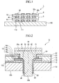
- FIG. 1 is a side cross-sectional view showing in schematic view a semiconductor device that has been obtained using the method for manufacturing a semiconductor device of the present invention.
- the reference symbol 1 in FIG. 1 indicates a semiconductor device 1.
- the semiconductor device 1 is formed by an interposer substrate (i.e., a connecting body) 100 and a plurality (two in FIG 1) of the same semiconductor chips 5.
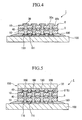
- the semiconductor chips 5 are provided with a semiconductor substrate 10 (i.e., a substrate) and trans-substrate conductive plugs 30 that penetrate the semiconductor substrate 10.
- a semiconductor substrate 10 i.e., a substrate
- trans-substrate conductive plugs 30 that penetrate the semiconductor substrate 10.
- the interposer substrate 100 is used as a connecting body, however, this connecting body is not limited solely to the interposer substrate 100 and, as described below, the connecting body may also be formed by a different semiconductor chip that has the same structure as the semiconductor chips 5.
- the semiconductor substrate 10 is made of silicon and has a thickness of approximately 50 ⁇ m.
- the trans-substrate conductive plug 30 is provided via an insulating film 22 inside a through hole H4 that is formed in the semiconductor substrate 10.
- the through hole H4 is formed penetrating from the active surface 10a side of the semiconductor substrate 10 to the back surface 10b side thereof.
- the semiconductor substrate 10 is formed having an integrated circuit (not shown) formed by transistor and memory elements and by other electronic elements on the active surface 10a side thereof.
- An insulating film 12 is formed on the surface of the active surface 10a side, and an interlayer insulating film 14 made of borophosphosilicate glass (referred to below as BPSG) or the like is further formed on top of the insulating film 12.
- BPSG borophosphosilicate glass
- a lead-free solder such as, for example, tin/silver or the like is used for the solder layer 40.
- methods that may be used to form the solder layer 40 include wet plating methods such as electrolytic plating, immersion plating, and electroless plating, chemical vapor deposition (CVD) methods such as thermal CVD, plasma CVD, and laser CVD, dry plating methods such as vacuum evaporation, sputtering, and ion plating, and thermal spraying, metal foil bonding, and the like.
- CVD chemical vapor deposition
- dry plating methods such as vacuum evaporation, sputtering, and ion plating
- thermal spraying metal foil bonding, and the like.
- metal foil bonding and the like.
- wet plating methods are particularly preferable.
- the solder layer 40 can be formed easily according to a wet plating method.
- solder layer 40 lead-free solder is used for the solder layer 40, however, it is also possible to use a metal paste or molten paste instead of this.
- An electrode pad 16 is formed in a predetermined location on the surface of the interlayer insulating film 14.
- This electrode pad 16 is formed by stacking in the following sequence a first layer 16a that is made of titanium (Ti) or the like, a second layer 16b that is made of titanium nitride (TiN) or the like, a third layer 16c that is made of aluminum/copper (AlCu) or the like, and a fourth layer 16d that is made of titanium nitride (TiN) or the like.
- the constituent materials of this electrode pad 16 can be suitably altered in accordance with the electrical characteristics, physical characteristics, and chemical characteristics that are required in the electrode pad 16. For example, it is also possible to form the electrode pad 16 using only Al, which is generally used as an electrode for integration purposes, or to form the electrode pad 16 using only copper which has low electrical resistance.
- electrode pads 16 are formed in a row in a peripheral portion of the semiconductor device 1, or else are formed in a row in a center portion of the semiconductor device 1. No integrated circuit is formed beneath these electrode pads 16.
- a passivation film 18 is formed on a surface of the interlayer insulating film 14 so as to cover these electrode pads 16.
- the passivation film 18 is made of silicon oxide, silicon nitride, or a polyimide resin and is formed having a thickness of, for example, approximately 1 ⁇ m. Note that, as described below, the electrode pads 16 are in contact with each other as a result of their being covered by at least a portion of the active surface side terminal portions 30a so as to be in an electrically connected state.
- an opening H1 in the passivation film 18 is formed in a center portion of the electrode pad 16, and an opening H2 is also formed in the electrode pad 16.
- the inner diameter of the opening H1 is formed at approximately 100 ⁇ m, while the inner diameter of the opening H2 is formed approximately 60 ⁇ m smaller than the inner diameter of the opening H1.
- An insulating film 20 made of SiO 2 or the like is formed on a surface of the passivation film 18 and on inner surfaces of the opening H1 and the opening H2.
- the inner diameter of the hole H3 is smaller than the inner diameter of the opening H2 and is formed at, for example, approximately 50 ⁇ m.
- the hole H3 has a circular shape when seen in plan view, however, it is not limited to this and may also have, for example, a rectangular shape when seen in plan view.
- An insulating film 22 made of SiO 2 or the like is formed on an inner wall surface of the hole H3 and on the surface of the insulating film 20.
- This insulating film 22 is provided in order to prevent the occurrence of current leaks, as well as corrosion and the like caused by oxygen or moisture or the like and, in the present embodiment, is formed having a thickness of approximately 1 ⁇ m.
- one end side of the insulating film 22 is in a state of protruding from the back surface 10b of the semiconductor substrate 10 particularly on the side that covers the inner wall surface of the hole H3.
- a portion of the insulating film 20 and insulating film 22 that are formed on the third surface 16c of the electrode pad 16 is removed along the circumferential edge of the opening H2, and an underlying film 24 is formed on the exposed surface of the third layer 16c of the electrode pad 16 and on the exposed surface (i.e., the inner surface) of the insulating layer 22.
- the underlying film 24 is composed of a barrier layer (i.e., a barrier metal) that is formed on a surface (i.e., an inner surface) of the insulating film 22 and the like, and by a seed layer (i.e., a seed electrode) that is formed on a surface (i.e., an inner surface) of the barrier layer.
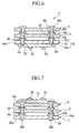
- the bonding tool 41 when applying heat and pressure using the bonding tool 41, the interposer substrate 100 on which the semiconductor chips 5 have been stacked is placed on the bonding stage 42. At this time, the bonding tool 41 is in a state of being heated to a temperature that enables it to melt the solder layers 40 and the solder layers 111, which are described below.
- the heat is conducted from the back surface side terminals 30b of the semiconductor chip 5 of the second layer to the solder layers 40 of the semiconductor chip 5 of the first layer so that an alloy layer is formed at the interface between the solder layers 40 and the back surface side terminals 30b.
- the solder layers 40 form an alloy layer at the interface with the active surface side terminals 30a of the first layer so that a reliable connection between the two is formed.
- the solder forms an alloy layer at the interface between the back surface side terminals 30b and the solder layers 111 as a result of the heat being conducted from the back surface side terminals 30b of the semiconductor chip 5 of the first layer to the solder layers 111. Accordingly, the semiconductor chip 5 of the first layer and the pads 110 of the interposer substrate 100 are reliably connected by an alloy layer.
- the heating of the bonding tool 41 by the heat source is terminated, and the solder layers 40 and the solder layers 111 are once again solidified (i.e., hardened). Accordingly, the semiconductor chip 5 that is the first layer is stacked via the solder layers 111 on the interposer substrate 100, and the semiconductor chip 5 that is the second layer is also reliably bonded via the solder layers 40 onto this first semiconductor chip 5.
- the semiconductor chips 5 can be held and fixed stably on the interposer substrate 100 while, at the same time, locations other than the bonds between terminals can be insulated.
- the stacked body that is formed by the semiconductor chips 5 being stacked on top of the interposer substrate 100 is removed from the bonding apparatus 4 so that the semiconductor device 1 shown in FIG. 1 is obtained.
- heat and pressure are applied to the semiconductor chips 5 that are stacked into a single body so as to bond them onto the interposer substrate 100, however, it is also possible to apply heat and pressure to each single layer of semiconductor chips 5 so that these are stacked reliably layer by layer.
- the bonding tool 41 when heat and pressure are applied by the bonding tool 41, if the solder layers 40 are formed on the active surface side terminals 30a, the solder layers 40 are melted. Therefore, the semiconductor chips 5 can be stacked by once again forming the solder layers 40 on top of the active surface side terminals 30a on which the solder layers 40 have already melted.
- the heat can be efficiently used to melt, via the back surface side terminals 30b, the solder layers 111 that are provided on the pads 110 of the interposer substrate 100. Accordingly, by efficiently using heat, bonding can be achieved at the melting temperature of the solder layers 111. Moreover, it is possible to lower the melting temperature of the solder compared with when the active surface side terminals 30a are stacked facing downwards, and damage to the insulating film 24 that covers the trans-substrate conductive plug 30 can be reduced.
- solder layers 111 have been connected via alloy layers to both the back surface side terminals 30b and the pads 110, and the back surface side terminals 30b and the pads 110 have been reliably bonded, the solder layers 111 are hardened. Therefore, it is possible to obtain excellent solder bonds.
- the active surface side terminals 30a are stacked facing upwards on the interposer substrate 100, when the solder layers 40 are melted on top of the active surface side terminals 30a, the solder layers 40 that are provided on the active surface side terminals 30a are not affected by gravity and made to droop down. Consequently, it is possible to prevent short-circuiting between vertically adjacent semiconductor chips 5 that is caused by the solder drooping down.
- the semiconductor chips 5 are bonded by being heated and compressed one layer at a time, because it is possible to reliably stack the semiconductor chips layer by layer, the reliability of the semiconductor device that is manufactured can be improved.
- the semiconductor chips 5 are heated and compressed as a single body, because the stacked semiconductor chips 5 can be bonded as a single body, the number of steps required to manufacture the semiconductor device 1 can be decreased and the productivity improved.
- solder forms alloy layers at the interfaces of connecting portions between the respective terminals and thereby forms a bond, the reliability of the bond portions can be improved.
- the active surface side terminals 30a are electrically connected to a portion of the electrode pads 16 as a result of at least a portion of the active surface side terminals 30a covering the electrode pads 16, it is possible to increase the electrical contact area when conductivity with the electrode pads 16 is obtained via the active surface side terminals 30a. Accordingly, when obtaining conductivity with the electrode pads 16, by eliminating wiring formation areas on the semiconductor substrate 10 that are connected to the electrode pads 16, a reduction in the size of the semiconductor substrate 10 can be achieved, and a reduction in the size of the semiconductor device 1 that is provided with the semiconductor substrate 10 can also be achieved.
- the sealing resin 180 is provided between semiconductor chips 5 that are connected via the solder layers 40 and between the semiconductor chip 5' in the electronic component 150.
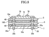
- FIG. 6 is a cross-sectional view showing a state in which semiconductor chips 5 are stacked on a substrate 60 that is subjected to a wafer level chip scale package (W-CSP) process using W-CSP technology as a connecting body.
- W-CSP wafer level chip scale package
- the semiconductor device 2 is constructed by stacking on the W-CSP processed substrate 60 a plurality (two layers in FIG 6) of semiconductor chips that have the same structure as the semiconductor chip 5 used in the above-described embodiment.
- the semiconductor chip 5 is connected to connection terminals that are formed on the W-CSP processed substrate 60 (described below) with the back surface side terminals 30b of the semiconductor chip 5 facing downwards.
- the W-CSP technology is a technology in which a wafer is diced to separate semiconductor chips after a formation of a redistribution layer (i.e., are rewiring) and a resin sealing on the wafer.
- solder layers 65 that are used to make connections with the back surface side terminals 30b of the semiconductor chip 5 are formed on the active surface side connecting electrodes 64a that protrude from the active surface 62a side of the substrate 62.
- the semiconductor chip 5 of the first layer is positioned on the solder layers 65 with the back surface side terminals 30b of the semiconductor chip 5 of the first layer facing downwards and the active surface side connecting electrodes 30a thereof facing upwards. At this time, it is also possible to temporarily fix the semiconductor chip 5 onto the top of the W-CSP processed substrate 60 by applying heat and pressure such that the positioned semiconductor chip 5 does not shift.
- the semiconductor chips 5 After the semiconductor chips 5 have been positioned and temporarily fixed onto the W-CSP processed substrate 60, using, for example, the bonding apparatus 4 or the like, the semiconductor chips 5 can be bonded using solder as a single body and stacked on the W-CSP processed substrate 60 by applying heat and pressure from the active surface side terminals 30a side of the stacked semiconductor chips 5.
- the semiconductor chips 5 are stacked on the W-CSP processed substrate 60 with the back surface side terminals 30b of the trans-substrate conductive plugs 30 of the semiconductor chips 5 facing downwards, and, in the same manner as in the above-described embodiment, heat is applied from the active surface side terminals 30a side using the heat source of the bonding tool 41. Accordingly, the heat is conducted from the active surface side terminals 30a, which have a larger outer shape, of the semiconductor chips 5 to the back surface side terminals 30b, which have a small outer shape.
- the surface area of the back surface side terminals 30b is smaller than that of the active surface side terminals 30a, only a small amount of heat conducts to peripheral portions of the back surface side terminals 30b, and the heat can be efficiently used to melt the solder layers 65 that are provided on the connecting electrodes 64 of the W-CSP processed substrate 60 via the back surface side terminals 30b.
- the heat that is applied to the semiconductor chips 5 can be set to approximately the melting temperature of the solder, so that damage to the insulating film 24 that covers the trans-substrate conductive plugs 30 of the semiconductor chips 5 can be reduced.
- the reliability of the semiconductor chips 5 is improved and the reliability of the semiconductor device 2 on which these semiconductor chips 5 have been stacked can be improved.
- solder layers 40 and the solder layers 65 form alloy layers at the interfaces with the respective connecting electrode portions and thereby form bonds, highly reliable bond portions can be formed.
- the range of the technology of the present invention is not limited to the above embodiment and various modifications can be made without departing from the spirit or scope of the present invention.
- a description is given of a semiconductor device 1 that is obtained by stacking two layers of semiconductor chips 5, however, the semiconductor device 1 can also be constructed by stacking three or more layers of semiconductor chips.
- a semiconductor chip 7 that has the same structure as that of the semiconductor chips 5 is used as the connecting body.
- a brazing material is provided on a first terminal of this semiconductor chip 7, and this first terminal is electrically connected via the brazing material to a second terminal of the semiconductor chip 5 that is stacked on top of the semiconductor chip 7.
- the semiconductor chip 5 on which a redistribution layer has been formed on an active surface 10a side by W-CSP processing has the same structure as the semiconductor chips 5 in the above-described embodiments apart from the fact that this a redistribution layer is formed thereon. Accordingly, the description below is given with the same descriptive reference symbols being used for the same structures.
- FIG. 7 shows a side cross-sectional view of a semiconductor device 3 of the present embodiment.
- the semiconductor chip 7 that is used as the connecting body is formed as the bottommost layer (i.e., on the bottom side in FIG. 7).
- a redistribution layer is formed by W-CSP processing on the active surface 10a side of the semiconductor chip 5 that forms the topmost layer (i.e., on the top side in FIG. 7) from among the plurality of stacked semiconductor chips 5. Note that, in the manufacturing steps described below, a semiconductor chip 5 is stacked on top of the semiconductor chip 7 which serves as the connecting body.
- a solder layer (i.e., a brazing material) 40 is provided on the active surface side terminals 30a of the semiconductor chip 7 that serves as a connecting body. These active surface side terminals 30a and the back surface side terminals 30b of the semiconductor chip 5 that is stacked on top of the semiconductor chip 7 are electrically connected via the solder layers 40. Note that, in the present embodiment, a structure is employed in which two layers of the semiconductor chips 5 are stacked on top of the semiconductor chip 7, which serves as a connecting body, however, the present invention is not limited to this and it is also possible to employ a structure in which two or more layers of the semiconductor chips 5 are stacked.
- a redistribution layer (not shown) is formed by W-CSP processing on the active surface 10a side of the topmost semiconductor chip 5, and this redistribution layer is connected to the active surface side terminals 30a that protrude on the active surface 10a side.
- the opposite side of the wiring portion that is connected to the active surface side terminals 30a is connected to bumps 70 that form external connection terminals. These bumps 70 are placed in desired positions, and the pitch and layout of the active surface side terminals 30a of the semiconductor chips 5 are modified (i.e., the wiring is redistributed) by connecting the bumps 70 and the active surface side terminals 30a using this wiring portion.
- the reference symbol 72 is a stress buffer layer that is formed in order to relieve any stress on the redistribution layer that is imparted through the bumps 70.
- the semiconductor chips 5 after the semiconductor chips 5 have been positioned or temporarily fixed onto the semiconductor chip 7, using, for example, the above-described bonding apparatus 4 or the like, the semiconductor chips 5 can be bonded using solder as a single body and stacked on the semiconductor chip 7 by applying heat and pressure from the active surface 10a side on the topmost layer, namely, from the surface side on which the redistribution layer has been formed by W-CSP processing. At this time, the applied heat is conducted from the active surface side terminals 30a of the semiconductor chips 5 that have undergone W-CSP processing to the back surface side terminals 30b thereof. The heat is then conducted in sequence from these back surface side terminals 30b to the active surface side terminals 30a of the semiconductor chip 5 forming the layer below.
- the semiconductor device 3 can also be used as a semiconductor device that is provided with a plurality of semiconductor chips that are stacked on top of a semiconductor chip 5 that has undergone W-CSP processing.
- heat is conducted from the back surface side terminals 30b that have a small outer shape to the active surface side terminals 30a that have a large outer shape.
- the heat conducts through the trans-substrate conductive plugs 30 so that, in the same manner, an alloy layer is formed in the bond portions of the semiconductor chip 5 forming the next layer down and a bond is obtained.
Landscapes
- Wire Bonding (AREA)
- Internal Circuitry In Semiconductor Integrated Circuit Devices (AREA)
Applications Claiming Priority (2)
| Application Number | Priority Date | Filing Date | Title |
|---|---|---|---|
| JP2004251809 | 2004-08-31 | ||
| JP2005114403 | 2005-04-12 |
Publications (2)
| Publication Number | Publication Date |
|---|---|
| EP1630867A2 true EP1630867A2 (fr) | 2006-03-01 |
| EP1630867A3 EP1630867A3 (fr) | 2010-06-02 |
Family
ID=35276360
Family Applications (1)
| Application Number | Title | Priority Date | Filing Date |
|---|---|---|---|
| EP05016769A Withdrawn EP1630867A3 (fr) | 2004-08-31 | 2005-08-02 | Procédé pour la fabrication d'un dispositif semi-conducteur et dispositif semi-conducteur |
Country Status (4)
| Country | Link |
|---|---|
| US (1) | US7491582B2 (fr) |
| EP (1) | EP1630867A3 (fr) |
| KR (1) | KR20060053168A (fr) |
| TW (1) | TWI272712B (fr) |
Cited By (1)
| Publication number | Priority date | Publication date | Assignee | Title |
|---|---|---|---|---|
| EP1818987A1 (fr) * | 2006-02-10 | 2007-08-15 | ELMOS Semiconductor AG | Agencement de composant semi-conducteur |
Families Citing this family (42)
| Publication number | Priority date | Publication date | Assignee | Title |
|---|---|---|---|---|
| US8084866B2 (en) * | 2003-12-10 | 2011-12-27 | Micron Technology, Inc. | Microelectronic devices and methods for filling vias in microelectronic devices |
| US20050247894A1 (en) | 2004-05-05 | 2005-11-10 | Watkins Charles M | Systems and methods for forming apertures in microfeature workpieces |
| US7232754B2 (en) | 2004-06-29 | 2007-06-19 | Micron Technology, Inc. | Microelectronic devices and methods for forming interconnects in microelectronic devices |
| SG120200A1 (en) | 2004-08-27 | 2006-03-28 | Micron Technology Inc | Slanted vias for electrical circuits on circuit boards and other substrates |
| US7300857B2 (en) | 2004-09-02 | 2007-11-27 | Micron Technology, Inc. | Through-wafer interconnects for photoimager and memory wafers |
| US7795134B2 (en) | 2005-06-28 | 2010-09-14 | Micron Technology, Inc. | Conductive interconnect structures and formation methods using supercritical fluids |
| US7622377B2 (en) * | 2005-09-01 | 2009-11-24 | Micron Technology, Inc. | Microfeature workpiece substrates having through-substrate vias, and associated methods of formation |
| US7863187B2 (en) * | 2005-09-01 | 2011-01-04 | Micron Technology, Inc. | Microfeature workpieces and methods for forming interconnects in microfeature workpieces |
| US7262134B2 (en) | 2005-09-01 | 2007-08-28 | Micron Technology, Inc. | Microfeature workpieces and methods for forming interconnects in microfeature workpieces |
| TWI341570B (en) * | 2006-03-17 | 2011-05-01 | Phoenix Prec Technology Corp | Laminated ic packaging substrate and connector structure |
| US7629249B2 (en) | 2006-08-28 | 2009-12-08 | Micron Technology, Inc. | Microfeature workpieces having conductive interconnect structures formed by chemically reactive processes, and associated systems and methods |
| US7902643B2 (en) | 2006-08-31 | 2011-03-08 | Micron Technology, Inc. | Microfeature workpieces having interconnects and conductive backplanes, and associated systems and methods |
| KR100845006B1 (ko) * | 2007-03-19 | 2008-07-09 | 삼성전자주식회사 | 적층 칩 패키지 및 그 제조 방법 |
| KR101213175B1 (ko) | 2007-08-20 | 2012-12-18 | 삼성전자주식회사 | 로직 칩에 층층이 쌓인 메모리장치들을 구비하는반도체패키지 |
| SG150410A1 (en) * | 2007-08-31 | 2009-03-30 | Micron Technology Inc | Partitioned through-layer via and associated systems and methods |
| US7880310B2 (en) * | 2007-09-28 | 2011-02-01 | Intel Corporation | Direct device attachment on dual-mode wirebond die |
| JP2009129953A (ja) * | 2007-11-20 | 2009-06-11 | Hitachi Ltd | 半導体装置 |
| KR100963617B1 (ko) * | 2007-11-30 | 2010-06-16 | 주식회사 하이닉스반도체 | 반도체 패키지 및 이의 제조 방법 |
| US7884015B2 (en) | 2007-12-06 | 2011-02-08 | Micron Technology, Inc. | Methods for forming interconnects in microelectronic workpieces and microelectronic workpieces formed using such methods |
| US7948095B2 (en) * | 2008-02-12 | 2011-05-24 | United Test And Assembly Center Ltd. | Semiconductor package and method of making the same |
| US8138577B2 (en) * | 2008-03-27 | 2012-03-20 | Hong Kong Applied Science And Technology Research Institute Co., Ltd. | Pulse-laser bonding method for through-silicon-via based stacking of electronic components |
| US7833895B2 (en) * | 2008-05-12 | 2010-11-16 | Texas Instruments Incorporated | TSVS having chemically exposed TSV tips for integrated circuit devices |
| KR20100045857A (ko) * | 2008-10-24 | 2010-05-04 | 삼성전자주식회사 | 반도체 칩, 스택 모듈, 메모리 카드 및 반도체 칩의 제조 방법 |
| JP5330863B2 (ja) * | 2009-03-04 | 2013-10-30 | パナソニック株式会社 | 半導体装置の製造方法 |
| KR20100109241A (ko) * | 2009-03-31 | 2010-10-08 | 삼성전자주식회사 | 칩 적층 패키지 및 그 제조방법 |
| KR101101922B1 (ko) * | 2010-04-22 | 2012-01-02 | 재단법인 서울테크노파크 | 적층형 반도체 패키지 및 그 제조방법 |
| KR101158730B1 (ko) * | 2010-07-15 | 2012-06-22 | 한국과학기술원 | 무전해도금을 이용한 적층 칩의 접합 방법 |
| JP2012039005A (ja) * | 2010-08-10 | 2012-02-23 | Toshiba Corp | 半導体装置およびその製造方法 |
| TWI462200B (zh) * | 2011-03-03 | 2014-11-21 | 日月光半導體製造股份有限公司 | 半導體封裝結構及其製作方法 |
| JP2012212786A (ja) * | 2011-03-31 | 2012-11-01 | Elpida Memory Inc | 半導体装置の製造方法 |
| JP2012256679A (ja) | 2011-06-08 | 2012-12-27 | Elpida Memory Inc | 半導体装置及びその製造方法 |
| US8896125B2 (en) | 2011-07-05 | 2014-11-25 | Sony Corporation | Semiconductor device, fabrication method for a semiconductor device and electronic apparatus |
| TWI495041B (zh) * | 2011-07-05 | 2015-08-01 | 新力股份有限公司 | 半導體裝置、用於半導體裝置之製造方法及電子設備 |
| US9105629B2 (en) | 2013-03-07 | 2015-08-11 | International Business Machines Corporation | Selective area heating for 3D chip stack |
| KR102084540B1 (ko) * | 2013-10-16 | 2020-03-04 | 삼성전자주식회사 | 반도체 패키지 및 그 제조방법 |
| KR102341750B1 (ko) | 2015-06-30 | 2021-12-23 | 삼성전자주식회사 | 반도체 패키지 및 이의 제조 방법 |
| CN121126834A (zh) * | 2015-12-18 | 2025-12-12 | 罗姆股份有限公司 | 半导体装置 |
| US10361140B2 (en) * | 2016-06-10 | 2019-07-23 | International Business Machines Corporation | Wafer stacking for integrated circuit manufacturing |
| US10418311B2 (en) * | 2017-03-28 | 2019-09-17 | Micron Technology, Inc. | Method of forming vias using silicon on insulator substrate |
| JP6685470B2 (ja) * | 2017-03-30 | 2020-04-22 | 三菱電機株式会社 | 半導体装置およびその製造方法、ならびに電力変換装置 |
| KR102440119B1 (ko) * | 2017-08-10 | 2022-09-05 | 삼성전자주식회사 | 반도체 패키지 및 그 제조방법 |
| TWI848733B (zh) * | 2023-06-02 | 2024-07-11 | 前源科技股份有限公司 | 電子元件的接合方法與巨量轉移電子元件的方法 |
Family Cites Families (22)
| Publication number | Priority date | Publication date | Assignee | Title |
|---|---|---|---|---|
| US5973396A (en) * | 1996-02-16 | 1999-10-26 | Micron Technology, Inc. | Surface mount IC using silicon vias in an area array format or same size as die array |
| US6882030B2 (en) * | 1996-10-29 | 2005-04-19 | Tru-Si Technologies, Inc. | Integrated circuit structures with a conductor formed in a through hole in a semiconductor substrate and protruding from a surface of the substrate |
| JP3537447B2 (ja) * | 1996-10-29 | 2004-06-14 | トル‐シ・テクノロジーズ・インコーポレイテッド | 集積回路及びその製造方法 |
| JP4011695B2 (ja) | 1996-12-02 | 2007-11-21 | 株式会社東芝 | マルチチップ半導体装置用チップおよびその形成方法 |
| JP4547728B2 (ja) | 1999-03-29 | 2010-09-22 | ソニー株式会社 | 半導体装置及びその製造方法 |
| JP2001308220A (ja) * | 2000-04-24 | 2001-11-02 | Nec Corp | 半導体パッケージ及びその製造方法 |
| JP3447690B2 (ja) | 2000-12-04 | 2003-09-16 | 日本電気株式会社 | 半導体チップの積層実装方法 |
| JP2002373957A (ja) * | 2001-06-14 | 2002-12-26 | Shinko Electric Ind Co Ltd | 半導体装置及びその製造方法 |
| US6975016B2 (en) * | 2002-02-06 | 2005-12-13 | Intel Corporation | Wafer bonding using a flexible bladder press and thinned wafers for three-dimensional (3D) wafer-to-wafer vertical stack integration, and application thereof |
| JP2003282819A (ja) | 2002-03-27 | 2003-10-03 | Seiko Epson Corp | 半導体装置の製造方法 |
| TWI229435B (en) * | 2002-06-18 | 2005-03-11 | Sanyo Electric Co | Manufacture of semiconductor device |
| JP3917484B2 (ja) | 2002-07-18 | 2007-05-23 | 富士通株式会社 | 半導体装置の製造方法および半導体装置 |
| JP3908148B2 (ja) | 2002-10-28 | 2007-04-25 | シャープ株式会社 | 積層型半導体装置 |
| JP3972813B2 (ja) * | 2002-12-24 | 2007-09-05 | セイコーエプソン株式会社 | 半導体装置の製造方法 |
| JP2004207416A (ja) | 2002-12-25 | 2004-07-22 | Seiko Epson Corp | 半導体装置、電子機器および半導体装置の製造方法 |
| JP2004221350A (ja) | 2003-01-15 | 2004-08-05 | Seiko Epson Corp | 半導体チップ、半導体ウエハ、半導体装置及びその製造方法、回路基板並びに電子機器 |
| JP4072677B2 (ja) | 2003-01-15 | 2008-04-09 | セイコーエプソン株式会社 | 半導体チップ、半導体ウエハ、半導体装置及びその製造方法、回路基板並びに電子機器 |
| JP4009846B2 (ja) | 2003-01-15 | 2007-11-21 | セイコーエプソン株式会社 | 半導体装置及びその製造方法、回路基板並びに電子機器 |
| JP2004297019A (ja) * | 2003-03-28 | 2004-10-21 | Seiko Epson Corp | 半導体装置、回路基板及び電子機器 |
| JP2005011838A (ja) * | 2003-06-16 | 2005-01-13 | Toshiba Corp | 半導体装置及びその組立方法 |
| KR100537892B1 (ko) | 2003-08-26 | 2005-12-21 | 삼성전자주식회사 | 칩 스택 패키지와 그 제조 방법 |
| JP5332133B2 (ja) | 2007-05-11 | 2013-11-06 | 株式会社リコー | 転写定着装置、及び画像形成装置 |
-
2005
- 2005-07-26 US US11/190,028 patent/US7491582B2/en not_active Expired - Lifetime
- 2005-07-27 TW TW094125418A patent/TWI272712B/zh not_active IP Right Cessation
- 2005-08-02 EP EP05016769A patent/EP1630867A3/fr not_active Withdrawn
- 2005-08-19 KR KR1020050076196A patent/KR20060053168A/ko not_active Ceased
Cited By (1)
| Publication number | Priority date | Publication date | Assignee | Title |
|---|---|---|---|---|
| EP1818987A1 (fr) * | 2006-02-10 | 2007-08-15 | ELMOS Semiconductor AG | Agencement de composant semi-conducteur |
Also Published As
| Publication number | Publication date |
|---|---|
| TWI272712B (en) | 2007-02-01 |
| KR20060053168A (ko) | 2006-05-19 |
| TW200616201A (en) | 2006-05-16 |
| EP1630867A3 (fr) | 2010-06-02 |
| US7491582B2 (en) | 2009-02-17 |
| US20060073637A1 (en) | 2006-04-06 |
Similar Documents
| Publication | Publication Date | Title |
|---|---|---|
| US7491582B2 (en) | Method for manufacturing semiconductor device and semiconductor device | |
| KR100827667B1 (ko) | 기판 내에 반도체 칩을 갖는 반도체 패키지 및 이를제조하는 방법 | |
| US9048225B2 (en) | Semiconductor device and method for manufacturing semiconductor device | |
| US8405199B2 (en) | Conductive pillar for semiconductor substrate and method of manufacture | |
| US7776653B2 (en) | Controlling flip-chip techniques for concurrent ball bonds in semiconductor devices | |
| US9263412B2 (en) | Packaging methods and packaged semiconductor devices | |
| CN110931479A (zh) | 半导体封装体 | |
| CN111403368B (zh) | 半导体封装体 | |
| CN101060088B (zh) | 半导体封装结构及其制造方法 | |
| CN108417550B (zh) | 半导体装置及其制造方法 | |
| US20110291267A1 (en) | Semiconductor wafer structure and multi-chip stack structure | |
| CN110085523A (zh) | 半导体器件以及其制造方法 | |
| US11063015B2 (en) | Semiconductor device package and method of manufacturing the same | |
| KR100842921B1 (ko) | 반도체 패키지의 제조 방법 | |
| US11935824B2 (en) | Integrated circuit package module including a bonding system | |
| CN110085560A (zh) | 迹线上凸块封装结构及其形成方法 | |
| CN115206897A (zh) | 包括模制层的半导体封装件 | |
| US12027494B2 (en) | Semiconductor device and manufacturing method thereof | |
| US8692390B2 (en) | Pyramid bump structure | |
| CN114725031A (zh) | 倒装芯片的封装结构 | |
| TWI757864B (zh) | 封裝結構及其形成方法 | |
| JP2007142026A (ja) | インターポーザとその製造方法及び半導体装置 | |
| US20210066208A1 (en) | Semiconductor package and method of manufacturing the same | |
| CN100435335C (zh) | 半导体装置的制造方法及半导体装置 | |
| US20240332194A1 (en) | Chip module assembly |
Legal Events
| Date | Code | Title | Description |
|---|---|---|---|
| PUAI | Public reference made under article 153(3) epc to a published international application that has entered the european phase |
Free format text: ORIGINAL CODE: 0009012 |
|
| AK | Designated contracting states |
Kind code of ref document: A2 Designated state(s): AT BE BG CH CY CZ DE DK EE ES FI FR GB GR HU IE IS IT LI LT LU LV MC NL PL PT RO SE SI SK TR |
|
| AX | Request for extension of the european patent |
Extension state: AL BA HR MK YU |
|
| PUAL | Search report despatched |
Free format text: ORIGINAL CODE: 0009013 |
|
| AK | Designated contracting states |
Kind code of ref document: A3 Designated state(s): AT BE BG CH CY CZ DE DK EE ES FI FR GB GR HU IE IS IT LI LT LU LV MC NL PL PT RO SE SI SK TR |
|
| AX | Request for extension of the european patent |
Extension state: AL BA HR MK YU |
|
| STAA | Information on the status of an ep patent application or granted ep patent |
Free format text: STATUS: THE APPLICATION HAS BEEN WITHDRAWN |
|
| 18W | Application withdrawn |
Effective date: 20101207 |