EP1630878A2 - GaN-Substrat und Halbleitervorrichtung hergestellt durch epitaktisches Wachstum auf das GaN-Substrat - Google Patents
GaN-Substrat und Halbleitervorrichtung hergestellt durch epitaktisches Wachstum auf das GaN-Substrat Download PDFInfo
- Publication number
- EP1630878A2 EP1630878A2 EP05255182A EP05255182A EP1630878A2 EP 1630878 A2 EP1630878 A2 EP 1630878A2 EP 05255182 A EP05255182 A EP 05255182A EP 05255182 A EP05255182 A EP 05255182A EP 1630878 A2 EP1630878 A2 EP 1630878A2
- Authority
- EP
- European Patent Office
- Prior art keywords
- layer
- type
- semiconductor
- gan substrate
- degree
- Prior art date
- Legal status (The legal status is an assumption and is not a legal conclusion. Google has not performed a legal analysis and makes no representation as to the accuracy of the status listed.)
- Granted
Links
Images






Classifications
-
- H—ELECTRICITY
- H10—SEMICONDUCTOR DEVICES; ELECTRIC SOLID-STATE DEVICES NOT OTHERWISE PROVIDED FOR
- H10P—GENERIC PROCESSES OR APPARATUS FOR THE MANUFACTURE OR TREATMENT OF DEVICES COVERED BY CLASS H10
- H10P14/00—Formation of materials, e.g. in the shape of layers or pillars
- H10P14/20—Formation of materials, e.g. in the shape of layers or pillars of semiconductor materials
-
- H—ELECTRICITY
- H10—SEMICONDUCTOR DEVICES; ELECTRIC SOLID-STATE DEVICES NOT OTHERWISE PROVIDED FOR
- H10H—INORGANIC LIGHT-EMITTING SEMICONDUCTOR DEVICES HAVING POTENTIAL BARRIERS
- H10H20/00—Individual inorganic light-emitting semiconductor devices having potential barriers, e.g. light-emitting diodes [LED]
- H10H20/80—Constructional details
- H10H20/81—Bodies
- H10H20/822—Materials of the light-emitting regions
- H10H20/824—Materials of the light-emitting regions comprising only Group III-V materials, e.g. GaP
- H10H20/825—Materials of the light-emitting regions comprising only Group III-V materials, e.g. GaP containing nitrogen, e.g. GaN
-
- C—CHEMISTRY; METALLURGY
- C30—CRYSTAL GROWTH
- C30B—SINGLE-CRYSTAL GROWTH; UNIDIRECTIONAL SOLIDIFICATION OF EUTECTIC MATERIAL OR UNIDIRECTIONAL DEMIXING OF EUTECTOID MATERIAL; REFINING BY ZONE-MELTING OF MATERIAL; PRODUCTION OF A HOMOGENEOUS POLYCRYSTALLINE MATERIAL WITH DEFINED STRUCTURE; SINGLE CRYSTALS OR HOMOGENEOUS POLYCRYSTALLINE MATERIAL WITH DEFINED STRUCTURE; AFTER-TREATMENT OF SINGLE CRYSTALS OR A HOMOGENEOUS POLYCRYSTALLINE MATERIAL WITH DEFINED STRUCTURE; APPARATUS THEREFOR
- C30B25/00—Single-crystal growth by chemical reaction of reactive gases, e.g. chemical vapour-deposition growth
- C30B25/02—Epitaxial-layer growth
- C30B25/18—Epitaxial-layer growth characterised by the substrate
-
- C—CHEMISTRY; METALLURGY
- C30—CRYSTAL GROWTH
- C30B—SINGLE-CRYSTAL GROWTH; UNIDIRECTIONAL SOLIDIFICATION OF EUTECTIC MATERIAL OR UNIDIRECTIONAL DEMIXING OF EUTECTOID MATERIAL; REFINING BY ZONE-MELTING OF MATERIAL; PRODUCTION OF A HOMOGENEOUS POLYCRYSTALLINE MATERIAL WITH DEFINED STRUCTURE; SINGLE CRYSTALS OR HOMOGENEOUS POLYCRYSTALLINE MATERIAL WITH DEFINED STRUCTURE; AFTER-TREATMENT OF SINGLE CRYSTALS OR A HOMOGENEOUS POLYCRYSTALLINE MATERIAL WITH DEFINED STRUCTURE; APPARATUS THEREFOR
- C30B25/00—Single-crystal growth by chemical reaction of reactive gases, e.g. chemical vapour-deposition growth
- C30B25/02—Epitaxial-layer growth
- C30B25/18—Epitaxial-layer growth characterised by the substrate
- C30B25/20—Epitaxial-layer growth characterised by the substrate the substrate being of the same materials as the epitaxial layer
-
- C—CHEMISTRY; METALLURGY
- C30—CRYSTAL GROWTH
- C30B—SINGLE-CRYSTAL GROWTH; UNIDIRECTIONAL SOLIDIFICATION OF EUTECTIC MATERIAL OR UNIDIRECTIONAL DEMIXING OF EUTECTOID MATERIAL; REFINING BY ZONE-MELTING OF MATERIAL; PRODUCTION OF A HOMOGENEOUS POLYCRYSTALLINE MATERIAL WITH DEFINED STRUCTURE; SINGLE CRYSTALS OR HOMOGENEOUS POLYCRYSTALLINE MATERIAL WITH DEFINED STRUCTURE; AFTER-TREATMENT OF SINGLE CRYSTALS OR A HOMOGENEOUS POLYCRYSTALLINE MATERIAL WITH DEFINED STRUCTURE; APPARATUS THEREFOR
- C30B29/00—Single crystals or homogeneous polycrystalline material with defined structure characterised by the material or by their shape
- C30B29/10—Inorganic compounds or compositions
- C30B29/40—AIIIBV compounds wherein A is B, Al, Ga, In or Tl and B is N, P, As, Sb or Bi
- C30B29/403—AIII-nitrides
- C30B29/406—Gallium nitride
-
- H—ELECTRICITY
- H10—SEMICONDUCTOR DEVICES; ELECTRIC SOLID-STATE DEVICES NOT OTHERWISE PROVIDED FOR
- H10D—INORGANIC ELECTRIC SEMICONDUCTOR DEVICES
- H10D30/00—Field-effect transistors [FET]
- H10D30/40—FETs having zero-dimensional [0D], one-dimensional [1D] or two-dimensional [2D] charge carrier gas channels
- H10D30/47—FETs having zero-dimensional [0D], one-dimensional [1D] or two-dimensional [2D] charge carrier gas channels having two-dimensional [2D] charge carrier gas channels, e.g. nanoribbon FETs or high electron mobility transistors [HEMT]
- H10D30/471—High electron mobility transistors [HEMT] or high hole mobility transistors [HHMT]
- H10D30/475—High electron mobility transistors [HEMT] or high hole mobility transistors [HHMT] having wider bandgap layer formed on top of lower bandgap active layer, e.g. undoped barrier HEMTs such as i-AlGaN/GaN HEMTs
- H10D30/4755—High electron mobility transistors [HEMT] or high hole mobility transistors [HHMT] having wider bandgap layer formed on top of lower bandgap active layer, e.g. undoped barrier HEMTs such as i-AlGaN/GaN HEMTs having wide bandgap charge-carrier supplying layers, e.g. modulation doped HEMTs such as n-AlGaAs/GaAs HEMTs
-
- H—ELECTRICITY
- H10—SEMICONDUCTOR DEVICES; ELECTRIC SOLID-STATE DEVICES NOT OTHERWISE PROVIDED FOR
- H10D—INORGANIC ELECTRIC SEMICONDUCTOR DEVICES
- H10D30/00—Field-effect transistors [FET]
- H10D30/80—FETs having rectifying junction gate electrodes
- H10D30/87—FETs having Schottky gate electrodes, e.g. metal-semiconductor FETs [MESFET]
-
- H—ELECTRICITY
- H10—SEMICONDUCTOR DEVICES; ELECTRIC SOLID-STATE DEVICES NOT OTHERWISE PROVIDED FOR
- H10D—INORGANIC ELECTRIC SEMICONDUCTOR DEVICES
- H10D62/00—Semiconductor bodies, or regions thereof, of devices having potential barriers
- H10D62/40—Crystalline structures
- H10D62/405—Orientations of crystalline planes
-
- H—ELECTRICITY
- H10—SEMICONDUCTOR DEVICES; ELECTRIC SOLID-STATE DEVICES NOT OTHERWISE PROVIDED FOR
- H10D—INORGANIC ELECTRIC SEMICONDUCTOR DEVICES
- H10D62/00—Semiconductor bodies, or regions thereof, of devices having potential barriers
- H10D62/80—Semiconductor bodies, or regions thereof, of devices having potential barriers characterised by the materials
- H10D62/82—Heterojunctions
- H10D62/824—Heterojunctions comprising only Group III-V materials heterojunctions, e.g. GaN/AlGaN heterojunctions
-
- H—ELECTRICITY
- H10—SEMICONDUCTOR DEVICES; ELECTRIC SOLID-STATE DEVICES NOT OTHERWISE PROVIDED FOR
- H10D—INORGANIC ELECTRIC SEMICONDUCTOR DEVICES
- H10D8/00—Diodes
-
- H—ELECTRICITY
- H10—SEMICONDUCTOR DEVICES; ELECTRIC SOLID-STATE DEVICES NOT OTHERWISE PROVIDED FOR
- H10H—INORGANIC LIGHT-EMITTING SEMICONDUCTOR DEVICES HAVING POTENTIAL BARRIERS
- H10H20/00—Individual inorganic light-emitting semiconductor devices having potential barriers, e.g. light-emitting diodes [LED]
- H10H20/01—Manufacture or treatment
- H10H20/011—Manufacture or treatment of bodies, e.g. forming semiconductor layers
- H10H20/013—Manufacture or treatment of bodies, e.g. forming semiconductor layers having light-emitting regions comprising only Group III-V materials
- H10H20/0137—Manufacture or treatment of bodies, e.g. forming semiconductor layers having light-emitting regions comprising only Group III-V materials the light-emitting regions comprising nitride materials
-
- H—ELECTRICITY
- H10—SEMICONDUCTOR DEVICES; ELECTRIC SOLID-STATE DEVICES NOT OTHERWISE PROVIDED FOR
- H10H—INORGANIC LIGHT-EMITTING SEMICONDUCTOR DEVICES HAVING POTENTIAL BARRIERS
- H10H20/00—Individual inorganic light-emitting semiconductor devices having potential barriers, e.g. light-emitting diodes [LED]
- H10H20/80—Constructional details
- H10H20/81—Bodies
- H10H20/817—Bodies characterised by the crystal structures or orientations, e.g. polycrystalline, amorphous or porous
-
- H—ELECTRICITY
- H10—SEMICONDUCTOR DEVICES; ELECTRIC SOLID-STATE DEVICES NOT OTHERWISE PROVIDED FOR
- H10P—GENERIC PROCESSES OR APPARATUS FOR THE MANUFACTURE OR TREATMENT OF DEVICES COVERED BY CLASS H10
- H10P14/00—Formation of materials, e.g. in the shape of layers or pillars
- H10P14/20—Formation of materials, e.g. in the shape of layers or pillars of semiconductor materials
- H10P14/24—Formation of materials, e.g. in the shape of layers or pillars of semiconductor materials using chemical vapour deposition [CVD]
-
- H—ELECTRICITY
- H10—SEMICONDUCTOR DEVICES; ELECTRIC SOLID-STATE DEVICES NOT OTHERWISE PROVIDED FOR
- H10P—GENERIC PROCESSES OR APPARATUS FOR THE MANUFACTURE OR TREATMENT OF DEVICES COVERED BY CLASS H10
- H10P14/00—Formation of materials, e.g. in the shape of layers or pillars
- H10P14/20—Formation of materials, e.g. in the shape of layers or pillars of semiconductor materials
- H10P14/29—Formation of materials, e.g. in the shape of layers or pillars of semiconductor materials characterised by the substrates
- H10P14/2901—Materials
- H10P14/2907—Materials being Group IIIA-VA materials
- H10P14/2908—Nitrides
-
- H—ELECTRICITY
- H10—SEMICONDUCTOR DEVICES; ELECTRIC SOLID-STATE DEVICES NOT OTHERWISE PROVIDED FOR
- H10P—GENERIC PROCESSES OR APPARATUS FOR THE MANUFACTURE OR TREATMENT OF DEVICES COVERED BY CLASS H10
- H10P14/00—Formation of materials, e.g. in the shape of layers or pillars
- H10P14/20—Formation of materials, e.g. in the shape of layers or pillars of semiconductor materials
- H10P14/29—Formation of materials, e.g. in the shape of layers or pillars of semiconductor materials characterised by the substrates
- H10P14/2926—Crystal orientations
-
- H—ELECTRICITY
- H10—SEMICONDUCTOR DEVICES; ELECTRIC SOLID-STATE DEVICES NOT OTHERWISE PROVIDED FOR
- H10P—GENERIC PROCESSES OR APPARATUS FOR THE MANUFACTURE OR TREATMENT OF DEVICES COVERED BY CLASS H10
- H10P14/00—Formation of materials, e.g. in the shape of layers or pillars
- H10P14/20—Formation of materials, e.g. in the shape of layers or pillars of semiconductor materials
- H10P14/32—Formation of materials, e.g. in the shape of layers or pillars of semiconductor materials characterised by intermediate layers between substrates and deposited layers
- H10P14/3202—Materials thereof
- H10P14/3214—Materials thereof being Group IIIA-VA semiconductors
- H10P14/3216—Nitrides
-
- H—ELECTRICITY
- H10—SEMICONDUCTOR DEVICES; ELECTRIC SOLID-STATE DEVICES NOT OTHERWISE PROVIDED FOR
- H10P—GENERIC PROCESSES OR APPARATUS FOR THE MANUFACTURE OR TREATMENT OF DEVICES COVERED BY CLASS H10
- H10P14/00—Formation of materials, e.g. in the shape of layers or pillars
- H10P14/20—Formation of materials, e.g. in the shape of layers or pillars of semiconductor materials
- H10P14/32—Formation of materials, e.g. in the shape of layers or pillars of semiconductor materials characterised by intermediate layers between substrates and deposited layers
- H10P14/3242—Structure
- H10P14/3244—Layer structure
- H10P14/3251—Layer structure consisting of three or more layers
- H10P14/3252—Alternating layers, e.g. superlattice
-
- H—ELECTRICITY
- H10—SEMICONDUCTOR DEVICES; ELECTRIC SOLID-STATE DEVICES NOT OTHERWISE PROVIDED FOR
- H10P—GENERIC PROCESSES OR APPARATUS FOR THE MANUFACTURE OR TREATMENT OF DEVICES COVERED BY CLASS H10
- H10P14/00—Formation of materials, e.g. in the shape of layers or pillars
- H10P14/20—Formation of materials, e.g. in the shape of layers or pillars of semiconductor materials
- H10P14/34—Deposited materials, e.g. layers
- H10P14/3402—Deposited materials, e.g. layers characterised by the chemical composition
- H10P14/3414—Deposited materials, e.g. layers characterised by the chemical composition being group IIIA-VIA materials
- H10P14/3416—Nitrides
-
- H—ELECTRICITY
- H10—SEMICONDUCTOR DEVICES; ELECTRIC SOLID-STATE DEVICES NOT OTHERWISE PROVIDED FOR
- H10P—GENERIC PROCESSES OR APPARATUS FOR THE MANUFACTURE OR TREATMENT OF DEVICES COVERED BY CLASS H10
- H10P14/00—Formation of materials, e.g. in the shape of layers or pillars
- H10P14/20—Formation of materials, e.g. in the shape of layers or pillars of semiconductor materials
- H10P14/34—Deposited materials, e.g. layers
- H10P14/3438—Doping during depositing
- H10P14/3441—Conductivity type
- H10P14/3442—N-type
-
- H—ELECTRICITY
- H10—SEMICONDUCTOR DEVICES; ELECTRIC SOLID-STATE DEVICES NOT OTHERWISE PROVIDED FOR
- H10P—GENERIC PROCESSES OR APPARATUS FOR THE MANUFACTURE OR TREATMENT OF DEVICES COVERED BY CLASS H10
- H10P14/00—Formation of materials, e.g. in the shape of layers or pillars
- H10P14/20—Formation of materials, e.g. in the shape of layers or pillars of semiconductor materials
- H10P14/34—Deposited materials, e.g. layers
- H10P14/3438—Doping during depositing
- H10P14/3448—Delta-doping
-
- H—ELECTRICITY
- H01—ELECTRIC ELEMENTS
- H01S—DEVICES USING THE PROCESS OF LIGHT AMPLIFICATION BY STIMULATED EMISSION OF RADIATION [LASER] TO AMPLIFY OR GENERATE LIGHT; DEVICES USING STIMULATED EMISSION OF ELECTROMAGNETIC RADIATION IN WAVE RANGES OTHER THAN OPTICAL
- H01S5/00—Semiconductor lasers
- H01S5/30—Structure or shape of the active region; Materials used for the active region
- H01S5/32—Structure or shape of the active region; Materials used for the active region comprising PN junctions, e.g. hetero- or double- heterostructures
- H01S5/3202—Structure or shape of the active region; Materials used for the active region comprising PN junctions, e.g. hetero- or double- heterostructures grown on specifically orientated substrates, or using orientation dependent growth
- H01S5/320275—Structure or shape of the active region; Materials used for the active region comprising PN junctions, e.g. hetero- or double- heterostructures grown on specifically orientated substrates, or using orientation dependent growth semi-polar orientation
-
- H—ELECTRICITY
- H01—ELECTRIC ELEMENTS
- H01S—DEVICES USING THE PROCESS OF LIGHT AMPLIFICATION BY STIMULATED EMISSION OF RADIATION [LASER] TO AMPLIFY OR GENERATE LIGHT; DEVICES USING STIMULATED EMISSION OF ELECTROMAGNETIC RADIATION IN WAVE RANGES OTHER THAN OPTICAL
- H01S5/00—Semiconductor lasers
- H01S5/30—Structure or shape of the active region; Materials used for the active region
- H01S5/32—Structure or shape of the active region; Materials used for the active region comprising PN junctions, e.g. hetero- or double- heterostructures
- H01S5/323—Structure or shape of the active region; Materials used for the active region comprising PN junctions, e.g. hetero- or double- heterostructures in AIIIBV compounds, e.g. AlGaAs-laser, InP-based laser
- H01S5/32308—Structure or shape of the active region; Materials used for the active region comprising PN junctions, e.g. hetero- or double- heterostructures in AIIIBV compounds, e.g. AlGaAs-laser, InP-based laser emitting light at a wavelength less than 900 nm
- H01S5/32341—Structure or shape of the active region; Materials used for the active region comprising PN junctions, e.g. hetero- or double- heterostructures in AIIIBV compounds, e.g. AlGaAs-laser, InP-based laser emitting light at a wavelength less than 900 nm blue laser based on GaN or GaP
-
- H—ELECTRICITY
- H10—SEMICONDUCTOR DEVICES; ELECTRIC SOLID-STATE DEVICES NOT OTHERWISE PROVIDED FOR
- H10D—INORGANIC ELECTRIC SEMICONDUCTOR DEVICES
- H10D62/00—Semiconductor bodies, or regions thereof, of devices having potential barriers
- H10D62/80—Semiconductor bodies, or regions thereof, of devices having potential barriers characterised by the materials
- H10D62/85—Semiconductor bodies, or regions thereof, of devices having potential barriers characterised by the materials being Group III-V materials, e.g. GaAs
- H10D62/8503—Nitride Group III-V materials, e.g. AlN or GaN
Definitions
- the present invention relates to a semiconductor substrate, or an epitaxial substrate, which includes a bulk GaN substrate and an epitaxially grown layer on the bulk GaN substrate, and semiconductor devices implemented by an epitaxial growth on the semiconductor substrate.
- the semiconductor devices include various semiconductor optical devices such as semiconductor light-emitting devices and various semiconductor electric devices such as transistors.
- III-V nitride compound semiconductors such as gallium nitride (GaN) have a wide bandgap. Utilizing properties and features of the wide bandgap semiconductors, high-brightness ultraviolet-blue/ green light-emitting diodes (LEDs) and blue-violet laser diodes and the like have been studied and developed. Moreover, high frequency/ high power III-V nitride compound semiconductor field-effect transistors (FETs) or the like have been fabricated based upon the properties and features of the wide bandgap semiconductors.
- LEDs ultraviolet-blue/ green light-emitting diodes
- FETs field-effect transistors
- GaN substrate a bulk GaN substrate
- epitaxially grown layer on the GaN substrate, the epitaxially grown layer having an improved surface flatness required for dimensions of a semiconductor device, a semiconductor device with high performance implemented by an epitaxial growth on the semiconductor substrate (epitaxial substrate).
- an aspect of the present invention may inhere in a semiconductor substrate, encompassing a GaN substrate having a surface, an orientation of which is defined by an absolute value of an off-angle of the surface from ⁇ 0001 ⁇ plane towards ⁇ 1-100> direction lying in a range of 0.12 degree to 0.35 degree and by an absolute value of an off-angle of the surface from ⁇ 0001 ⁇ plane towards ⁇ 11 ⁇ 20> direction lying in a range of 0.00 degree to 0.06 degree: and a single-crystal layer formed of III ⁇ V nitride compound semiconductor epitaxially grown on the surface of the GaN substrate.
- Another aspect of the present invention may inhere in a semiconductor light-emitting device, encompassing: a GaN substrate having a surface, an orientation of which is defined by an absolute value of an off-angle of the surface from ⁇ 0001 ⁇ plane towards ⁇ 1-100> direction lying in a range of 0.12 degree to 0.35 degree and by an absolute value of an off-angle of the surface from ⁇ 0001 ⁇ plane towards ⁇ 11-20> direction lying in a range of 0.00 degree to 0.06 degree; a single-crystal layer formed of III-V nitride compound semiconductor epitaxially grown on the surface of the GaN substrate; and a light-emitting layer formed of epitaxially grown III-V nitride compound semiconductor provided on the single-crystal layer.
- a still another aspect of the present invention may inhere in a semiconductor device, encompassing: a GaN substrate having a surface, an orientation of which is defined by an absolute value of an off-angle of the surface from ⁇ 0001 ⁇ plane towards ⁇ 1-100> direction lying in a range of 0.12 degree to 0.35 degree and by an absolute value of an off-angle of the surface from ⁇ 0001 ⁇ plane towards ⁇ 11-20> direction lying in a range of 0.00 degree to 0.06 degree; and a device-structure portion formed of epitaxially grown III-V nitride compound semiconductor provided on the GaN substrate.
- a "device-structure portion” does not necessarily mean an entire device-structure of a semiconductor electronic device or a semiconductor optical device as long as it includes a primary structure portion that bears the main operations of the semiconductor electronic device or the semiconductor optical device, such as a light emitting layer and a peripheral structure of the light emitting layer in a laser diode or an LED, a structure around a base region that controls the main current flowing between emitter and collector regions in a heterojunction bipolar transistor (HBT) and a structure around a channel layer through which the main current flowing between source and drain regions in a high electron mobility transistor (HEMT).
- HBT heterojunction bipolar transistor
- HEMT high electron mobility transistor
- the indicator "+” in the Figures indicates relatively strong doping and the indicator "-” in the Figures indicates relatively weak doping.
- Prepositions, such as “on” , “over” , “under” , “beneath” , and “normal” are defined with respect to a planar surface of the substrate, regardless of the orientation in which the substrate is actually held. A layer is on another layer even if there are intervening layers
- a semiconductor device is fabricated on a semiconductor substrate (11, 12) embracing an n-type GaN substrate 11 and an n-type GaN layer 12 grown on the n-type GaN substrate 11, the n-type GaN layer 12 is doped with n-type impurity atoms such as silicon (Si) atoms.
- the n-type GaN layer 12 is merely an example. More generally, the n-type GaN layer 12 may be an n-type single-crystal layer of another III-V nitride compound semiconductor such as an In x Ga 1-x-y Al y N layer.
- the n-type GaN substrate 11 has a surface orientation, which is defined by the absolute value of an off-angle ⁇ 1-100 of a surface from ⁇ 0001 ⁇ plane towards ⁇ 1-100> direction and absolute value of an off-angle ⁇ 11-20 of the surface from ⁇ 0001 ⁇ plane towards ⁇ 11-20> direction, where those absolute values are represented by: 0.12 degree ⁇
- ⁇ 1-100> direction represents a full set of equivalent directions such as [1-100], [10-10], [ ⁇ 1100], [-1010], [01 ⁇ 10], [0 ⁇ 110] directions in hexagonal symmetry
- ⁇ 11 ⁇ 20> direction represents a full set of equivalent directions such as [11-20], [1-210], [-2110], [ ⁇ 1 ⁇ 120], [-12-10], [2 ⁇ 1 ⁇ 10] directions in hexagonal symmetry.
- a device-structure portion of a laser diode is formed on the first stacked structure (11, 12) embracing the n-type GaN substrate 11 and the n-type GaN layer 12 grown on the n-type GaN substrate 11.
- the first stacked structure (11, 12) is referred as the "semiconductor substrate (11, 12)" , which may be referred as the “epitaxial substrate (11, 12)” in general, and the device-structure portion is successively grown through epitaxy on the semiconductor substrate (11, 12).
- the device-structure portion is implemented by a second stacked structure (13, 14, 15, 16, 17, 18, 19, 20) as a base structure encompassing an n-type cladding layer 13, an n-type GaN light-guiding layer 14 on the n-type cladding layer 13, an active layer (light-emitting layer) 15 on the n-type GaN light-guiding layer 14, a first p-type GaN light-guiding layer 16 on the active layer (light-emitting layer) 15, an overflow preventing layer 17 on the first p-type GaN light-guiding layer 16, a second p-type GaN light-guiding layer 18 on the overflow preventing layer 17, a p-type cladding layer 19 on the second p-type GaN light-guiding layer 18, and a p-type GaN contact layer 20 on the p-type cladding layer 19; wherein the n-type cladding layer 13 or the lowest layer contacts with the top surface of the n-type GaN layer 12 of the semiconductor substrate (11, 12).
- the "device-structure portion” means a principal structure that bears the main operations of the laser diode, which is implemented by the second stacked structure (13, 14, 15, 16, 17, 18, 19, 20) shown in FIG. 1 as a base structure, and does not include the first stacked structure (11, 12).
- the "device-structure portion” does not necessarily mean the entire device structure of an optical semiconductor as long as it includes a principal structure that bears the main operations of the semiconductor optical device.
- the n-type cladding layer 13 is a superlattice made up of an undoped Al 0.1 Ga 0.9 N layer and a GaN layer doped with approximately 1 x 10 18 cm -3 of n-type impurity atoms such as Si atoms, but is not limited to the superlattice, and may be a single layer film (approximate thickness of 1.5 micrometer) of an n-type III-V nitride compound semiconductor made of an Al 0.05 Ga 0.95 N layer or the like, for example.
- a superlattice made up of an undoped Al 0.1 Ga 0.9 N layer and a GaN layer doped with approximately 1 x 10 18 cm -3 of n-type impurity atoms is used; however, the effectiveness of the present invention do not change even if both the Al 0.1 Ga 0.9 N layer and the GaN layer are doped with n-type impurity atoms such as Si atoms.
- the n-type GaN light-guiding layer 14 is an approximately 0.1 ⁇ micrometer ⁇ thick GaN layer doped with approximately 1 x 10 18 cm -3 of n-type impurity atoms such as Si atoms; however, more generally, it may be an n-type III-V nitride compound semiconductor layer of In x Ga 1-x-y Al y N or the like.
- the active layer (light-emitting layer) 15 is implemented by a multi-quantum well (MQW) made up of three quantum well (QW) layers, which are made of approximately 3.5-nm-thick undoped In 0.1 Ga 0.9 N layers, and barrier layers, which are made of approximately 7-nm-thick undoped In 0.01 Ga 0.99 N layers, respectively, alternately stacked and sandwiching the quantum well.
- MQW multi-quantum well
- QW quantum well
- barrier layers which are made of approximately 7-nm-thick undoped In 0.01 Ga 0.99 N layers, respectively, alternately stacked and sandwiching the quantum well.
- the indium mole fraction x of the In x Ga 1-x N layers implementing the MQW is merely an example, and the effectiveness of the present invention do not change even if another value is used as long as the mole fraction x of the QW layer is greater than the mole fraction x of the barrier layer.
- In 0.08 Ga 0.92 N layers may be used for the
- the first p-type GaN light-guiding layer 16 provided on the active layer (light-emitting layer) 15 should be formed with a thickness of about 0.03 micrometer.
- the overflow preventing layer 17 is a layer for preventing overflow of electrons and is made of an approximately 10-nm-thick Al 0.2 Ga 0.8 N layer doped with approximately 5 x 10 18 cm -3 of p-type impurity atoms such as magnesium (Mg) atoms.
- the second p-type GaN light-guiding layer 18 is an approximately 0.1-micrometer-thick GaN layer doped with approximately 5 to 10 x 10 18 cm -3 of p-type impurity atoms such as Mg atoms; however, more generally, it may be a p-type III-V nitride compound semiconductor layer of In x Ga 1-x-y Al y N or the like.
- the p-type cladding layer 19 is a superlattice made up of an undoped Al 0.1 Ga 0.9 N layer and a GaN layer doped with p-type impurity atoms such as Mg atoms, but is not limited the superlattice, and may be a single layer film (approximate thickness of 0.6 micrometer) of a p-type III-V nitride compound semiconductor doped with approximately 1 x 10 19 cm -3 Mg concentration made of an Al 0.05 Ga 0.95 N layer or the like, for example.
- a superlattice made up of an undoped Al 0.1 Ga 0.9 N layer and a GaN layer doped with p-type impurity atoms is used; however, the effectiveness of the present invention do not change even if both the Al 0.1 Ga 0.9 N layer and the GaN layer are doped with p-type impurity atoms such as Mg atoms.
- the p-type GaN contact layer 20 is an approximately 0.05-micrometer-thick GaN layer doped with approximately 2 x 10 20 cm -3 of p-type impurity atoms such as Mg atoms; however, more generally, it may be a p-type III-V nitride compound semiconductor layer of In x Ga 1-x-y Al y N or the like.
- MOCVD metal-organic chemical vapor deposition
- a two-micrometer-width ridge structure is then formed in the top of the second stacked structure (13, 14, 15, 16, 17, 18, 19, 20), by etching process as a device fabrication process, so that the stacked structure of the p-type cladding layer 19 and the p-type GaN contact layer 20 has a protrusion at the center implementing the ridge structure.
- the p-type cladding layer 19 has a flat portion surrounding the protrusion at the center so as to establish the ridge structure.
- the p-type cladding layer 19 itself has a reverse-T-shaped step structure made of a protruded portion and a flat portion serving as a base for the protruded portion.
- the p-type GaN contact layer 20 is then provided on top of the protrusion made of the p-type cladding layer 19.
- the ridge structure implemented by the stacked protrusion, encompassing the p-type cladding layer 19 and the p-type GaN contact layer 20, extends perpendicular to the plane of the paper. Note that the ridge structure is not limited to a rectangular ridge having a cross-section with vertical sidewalls as shown in FIG. 1, and may form a trapezoidal ridge having mesa slants in a cross-sectional view.
- Insulating films 41 are provided as "current blocking layers” sandwiching the ridge structure (protrusion) on the p-type cladding layer 19, which forms a couple of flat portions surrounding the protrusion, and the current blocking layers prevent an laser oscillation at transverse mode. Thickness of the current blocking layers may be arbitrarily selected according to the design of the laser in a range from approximately 0.3 ⁇ m to 0.8 micrometer, and may be set to, for example, a value approximately 0.5 micrometer.
- the current blocking layers may be made of a high resistivity semiconductor layer such as an AlN layer or an Al 0.2 Ga 0.8 N layer, a proton irradiated semiconductor layer, a silicon oxide film (SiO 2 film), or a zirconium oxide film (ZrO 2 film).
- it may be a multilayer film made up of a SiO 2 film and a ZrO 2 film, for example.
- various materials having a lower refractive index than that of the III-V nitride compound semiconductor used for the active layer (light-emitting layer) 15 may be used for the current blocking layers.
- An n-type semiconductor layer such as n-type GaN or n-type Al y Ga 1-y N may be used as the current blocking layers instead of using the insulating film 41 against the ridge structure implemented by the p-type cladding layer 19 and the p-type GaN contact layer 20 so as to establish a pn-junction isolation.
- the Pd film is about 0.05 micrometer thick
- the Pt film is about 0.05 micrometer thick
- the Au film is about one micrometer thick, for example.
- An n-side electrode (cathode electrode) 31 made of a titanium- platinum- gold (Ti/ Pt/ Au) composite film is provided on the bottom surface of the n-type GaN substrate 11.
- the n-side electrode (cathode electrode) 31 may be implemented by about 0.05-micrometer-thick Ti film, about 0.05-micrometer-thick Pt film, and about one-micrometer-thick Au film. End faces of a laser resonator are formed by cleaving. A high-reflection coat film is applied on the rear-end face, which is the opposite side to the front-end face from which laser light is emitted.
- the n-type cladding layer 13, the n-type GaN light-guiding layer 14, the active layer (light-emitting layer) 15, the first p-type GaN light-guiding layer 16, the overflow preventing layer 17, the second p-type GaN light-guiding layer 18, the p-type cladding layer 19, and the p-type GaN contact layer 20 providing the device-structure portion are merely examples, and the present invention is not limited to these materials. More generally, an appropriate single-crystal layer of another III-V nitride compound semiconductor such as an In x Ga 1-x-y Al y N layer may be used depending upon the design choice.
- the indium mole fraction x of the In x Ga 1-x N layer and the aluminum mole fraction y of the Al y Ga 1-y N layer mentioned above should be understood as mere examples, and the following effectiveness may naturally be achieved even using other mole fraction values.
- FIG. 2 shows a current vs. light output power characteristics of the semiconductor device (laser diode) according to the first embodiment of the present invention under a continuous oscillation condition at 25 degrees Celsius, and compares with the current vs. light output power characteristics of a comparative example under the same condition.
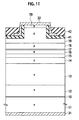
- the current vs. light output power characteristic indicated by a solid line in FIG. 2 is a result of a structure incorporating a ⁇ -doped layer 10 as shown in FIG. 11 on the GaN substrate 11 that has a surface orientation satisfying the relationship of Equations (1) and (2) in terms of off angles ⁇ 1-100 and ⁇ 11-20
- the average threshold current of the laser diode with ⁇ doped layer 10 is approximately 45 milliamperes.
- light output power characteristic indicated by a dashed-and - dotted line in FIG. 2 is a result of a structure without incorporating the ⁇ doped layer 10 as shown in FIG. 11 on the GaN substrate 11, but the GaN substrate 11 has a surface orientation satisfying the relationship of Equations (1) and (2) in terms of off angles ⁇ 1-100 and ⁇ 11-20 .
- the average threshold current of the laser diode without ⁇ -doped layer 10 is approximately 55 milliamperes.
- the average threshold current found from the current vs. light output power characteristics of the laser diode according to the comparative example is 106 milliamperes, and is higher than that for the semiconductor device according to the first embodiment.
- the higher average threshold current with the structure of the comparative example is due to occurrence of fluctuation of the flatness in the boundary surface through which light propagate. Therefore, it is understood that the structure of the comparative example establishes a wider gain distribution and increased energy loss than the structure of the first embodiment.
- FIGS. 3A and 3B show results of ⁇ /2 ⁇ scanning across (0002) plane.
- the peak at 0 arcsec shown on the right end of FIGS. 3A and 3B, corresponds to a diffraction from the GaN layer.
- the n-type cladding layer 13 is a superlattice made up of n-type Al 0.1 Ga 0.9 N layers and n-type GaN layers
- the p-type cladding layer 19 is a superlattice made up of p-type Al 0.1 Ga 0.9 N layers and p-type GaN layers
- two satellite peaks at a negative first order and a positive first order diffraction corresponding to the period of superlattice, for example, can be detected in addition to the peak at the zero order diffraction.
- the satellite peaks observed near -3200 arcsec in FIGS. 3A and 3B are the negative first order satellite peaks ascribable to the Al 0.1 Ga 0.9 N/ GaN superlattice.
- the full width at half maximum (FWHM) of the satellite peak for the wafer with the above-mentioned laser structure grown on the GaN substrate 11, which has a surface orientation satisfying the relationship of Equations (1) and (2) in terms of the off angles ⁇ 1-100 and ⁇ 11-20 is 145 arcsec.
- the FWHM of the satellite peak for the wafer with the above-mentioned laser structure grown on the ⁇ 0001 ⁇ -orientated GaN substrate 11 that does not satisfy the relationship of Equations (1) and (2) in terms of the off angles ⁇ 1-100 and ⁇ 11-20 is 367 arcsec, which is wide.
- the FWHM being wide means that the steepness at the superlattice interfaces and the surface flatness of the film, observing the entire area of the cladding layer, are poor.
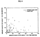
- FIG. 4 Results of observing the grown wafer through a Nomarski microscope are given in FIG. 4.
- absolute values of an off-angle ⁇ 1-100 of a surface from ⁇ 0001 ⁇ plane towards [1-100] direction are plotted along abscissa
- absolute values of an off-angle ⁇ 11-20 of the surface from ⁇ 0001 ⁇ plane towards [11-20] direction are plotted along ordinate.
- favorable flatness with which there is no giant step is observed within the range of the absolute values of the respective off-angles ⁇ 1-100 between 0.12 degree and 0.35 degree and within range of absolute values of the respective off-angles ⁇ 11-20 between 0.00 degree and 0.06 degree, as represented by symbols of open circle (O), open triangle ( ⁇ ) and open square ( ⁇ ).
- the absolute values of the respective off-angles ⁇ 1-100 lie within range of 0.12 degree and 0.30 degree and within range of absolute values of the respective off-angles ⁇ 11-20 between 0.00 degree and 0.06 degree, as represented by open triangle symbols and open circle symbols, because the FWHM of x-ray diffraction-rocking curve lie in a range of 200 to 250 arcsec and a flat surface can be obtained.
- the absolute values of the respective off ⁇ angles ⁇ 1-100 lie within range of 0.14 to and 0.28 degree and within range of absolute values of the respective off-angles ⁇ 11-20 between 0.00 degree and 0.06 degree, as represented by open circle symbols, because the FWHM of x-ray diffraction-rocking curve becomes approximately 150 arcsec and a mirror surface can be obtained without no presence of giant step.
- the GaN substrate 11 having the orientation of crystal plane satisfying the relationship of Equations (1) and (2) in terms of off angles ⁇ 1-100 and ⁇ 11-20 , achieves a very smooth mirror surface required for device dimensions, the surface morphology of the wafer, in which the laser structure is grown on the ⁇ 0001 ⁇ orientated GaN substrate 11 that do not satisfy the relationship of Equations (1) and (2) in terms of off angles ⁇ 1-100 and ⁇ 11-20 , establishes giant steps in the order of several ten to several hundred micrometer so as to form an uneven surface.
- the semiconductor substrate (epitaxial substrate) according to the first embodiment is grown on the GaN substrate 11, there are essentially few problems of defects such as threading dislocation and cracks in the epitaxially grown layer, the defects are ascribable to the lattice mismatch with the substrate. Also, since the orientation of crystal plane of the GaN substrate 11 is optimized, an epitaxially grown layer of a III-V nitride compound semiconductor with favorable surface morphology and surface flatness is obtained. Furthermore, the semiconductor device (laser diode) according to the first embodiment using the semiconductor substrate (epitaxial substrate) with excellent surface flatness facilitates fabrication of a waveguide with little optical loss, and provision of a reduced threshold current, an increased operating life, and improved reliability. In addition, according to the semiconductor device (laser diode) associated with the first embodiment, spatial expansion of gain distribution is prevented, thereby providing a high efficiency device.
- a fabrication method for the semiconductor device (laser diode), according to the first embodiment of the present invention is described with reference to FIGS. 5 through 11.
- the fabrication method for the semiconductor device described forthwith is merely an example, and the present invention may naturally be implemented using other various fabrication methods including various modifications.
- a crystal-growth furnace used in the semiconductor device (laser diode) fabrication method according to the first embodiment is described as an MOCVD furnace, but it may be fabricated by another method using another crystal-growth furnace such as a molecular beam epitaxy (MBE) furnace.
- MBE molecular beam epitaxy
- a semiconductor device (laser diode), according to a modification of the first embodiment of the present invention, is different from the semiconductor device according to the first embodiment of the present invention shown in FIG. 1 in that a stacked structure (11, 10, 12) of the n-type GaN layer 12 further encompasses a ⁇ -doped layer (delta-doped layer) 10.
- the ⁇ -doped layer 10 is grown on a GaN substrate 11 having a surface, an orientation of which is satisfying the relationship of Equations (1) and (2) in terms of off angles ⁇ 1-100 and ⁇ 11-20 .
- an n-type GaN layer 12 is grown on the GaN substrate 11 through the ⁇ -doped layer 10.
- the device-structure portion of a laser diode which is implemented by a stacked structure with the n-type cladding layer 13, the n-type GaN light-guiding layer 14, the active layer (light-emitting layer) 15, the first p-type GaN light-guiding layer 16, the overflow preventing layer 17, the second p-type GaN light-guiding layer 18, the p-type cladding layer 19, and the p-type GaN contact layer 20 in order
- the stacked structure is formed on the n-type GaN layer 12
- the structures of the ridge structure, an electrode and the like are similar to the structure and materials already explained in the first embodiment, with reference to FIG. 1, and overlapping or redundant description may be omitted in the modification of the first embodiment.
- the ⁇ doped layer 10 is a GaN layer approximately 200 nm thick or less doped with n-type impurity atoms such as Si atoms with a concentration of at least about 5 x 10 17 cm -3 and no greater than about 2 x 10 19 cm -3 , preferably at least about 1 x 10 18 cm -3 and no greater than about 2 x 10 19 cm -3 , even more preferably at least about 4 x 10 18 cm -3 and no greater than about 2 x 10 19 cm -3 .
- the thickness lower limit of the ⁇ -doped layer 10 is equivalent to an atomic layer thickness or approximately 0.3 nm.
- the thickness of the ⁇ -doped layer 10 should preferably fall within the range of an atomic layer thickness and about 150 nm, more preferably between about 5 nm and about 150 nm.
- the impurity concentration of the ⁇ -doped layer 10 exceeds about 2 x 10 19 cm -3 , the top surface of the n-type GaN layer 12 grown on the ⁇ -doped layer 10 becomes rough.
- the ⁇ -doped layer 10 doped with at least about 4 x 10 18 cm -3 and no greater than about 2 x 10 19 cm -3 of n-type impurity atoms such as Si atoms is formed to have a thickness ranging between an atomic layer thickness and about 200 nm as a favorable form
- the lateral crystal growth speed inward the substrate surface can be accelerated, improving flatness of the top surface of the epitaxially grown layer.
- the effects of the lateral crystal growth are not prominent when the impurity concentration falls below about 4 x 10 18 cm -3 .
- the effectiveness further decreases as the impurity concentration falls below about 1 x 10 18 cm -3 , and when the impurity concentration falls below about 5 x 10 17 cm -3 , acceleration of the lateral crystal growth speed and improvement in surface flatness are more difficult to achieve.
- the ⁇ -doped layer 10 is provided between the n-type GaN layer 12 and the n-type GaN substrate 11, thereby accelerating the lateral crystal growth speed along inward the n-type GaN substrate 11 surface.
- the acceleration of the lateral crystal growth facilitates improved flatness in the surface morphology of the resulting grown wafer compared to the semiconductor device without having the ⁇ -doped layer 10 according to the first embodiment shown in FIG. 1.
- the average threshold current of the semiconductor device (laser diode) according to the modification of the first embodiment, as shown in FIG. 2 is reduced to 45 milliamperes, the operating life is extended, and reliability is further improved.
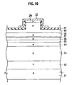
- the semiconductor device (laser diode) fabrication method according to the modification of the first embodiment, as shown in FIG. 12, when the n-type GaN layer 12 is deposited via the ⁇ -doped layer 10, on the GaN substrate 11 that has a surface orientation satisfying the relationship of Equations (1) and (2) in terms of off angles ⁇ 1-100 and ⁇ 11-20 , and the n-type cladding layer 13, the n-type GaN light-guiding layer 14, the active layer (light-emitting layer) 15, the first p-type GaN light-guiding layer 16, the overflow preventing layer 17, the second p-type GaN light-guiding layer 18, the p-type cladding layer 19, and the p-type GaN contact layer 20 are then epitaxially grown successively, the steps thereafter are substantially the same as the procedures shown in FIGS. 7 through 10, and repetitive descriptions thereof are omitted.
- a semiconductor device, according to the second embodiment of the present invention, as shown in FIG. 13, is the same as the semiconductor device already explained in the first embodiment in that the semiconductor device is formed on a first stacked structure (11, 12), which is implemented by a method such that growing an n-type GaN layer 12 on a GaN substrate 11, the GaN substrate 11 satisfies the relationship of Equations (1) and (2) in terms of off angles ⁇ 1-100 and ⁇ 11-20 .
- a device-structure portion implementing a light-emitting diode is formed upon the first stacked structure (11, 12).
- the n-type GaN layer 12 is merely an example. More generally, it may naturally be an n-type single-crystal layer of another III-V nitride compound semiconductor such as an In x Ga 1-x-y Al y N layer.
- an n-type cladding layer 13 made of a Si-doped Al 0.05 Ga 0.95 N layer is epitaxially grown directly on the n-type GaN layer 12 or the top layer of the first stacked structure (11, 12), and an active layer (light-emitting layer) 21 made of an In x Ga 1-x N layer, a p-type cladding layer 19 made of a Mg-doped Al 0.05 Ga 0.95 N layer, and a p-type GaN contact layer 20 made of a Mg-doped GaN layer are successively stacked in order upon the n-type cladding layer 13. Furthermore, on the p-type GaN contact layer 2, a transparent electrode implementing a p-side electrode (anode electrode) 33 is formed.
- a "device-structure portion” means a principal structure that bears the main operations of the LED, which is implemented by the second stacked structure (13, 21, 19, 20) shown in FIG. 13 as a base structure, and does not include the first stacked structure (11, 12) that serves as an n-type contact layer under the device-structure portion.
- the "device-structure portion” does not necessarily mean the entire device structure of an optical semiconductor as long as the device-structure portion includes a principal structure that bears the main operations of the semiconductor optical device, which is the same as those of the semiconductor device already explained in the first embodiment.
- the n-type cladding layer 13, the In x Ga 1-x N active layer 21, the p-type cladding layer 19, and the p-type GaN contact layer 20 forming the device-structure portion are merely an example, and the present invention is not limited to these materials.
- a single-crystal layer of another III-V nitride compound semiconductor such as an In x Ga 1-x-y Al y N layer is available for each layer forming the device-structure portion.
- the semiconductor substrate (epitaxial substrate) according to the second embodiment has the GaN substrate 11, there are essentially few problems of defects such as threading dislocation and cracks ascribable to the lattice mismatch between the epitaxially grown layer and the GaN substrate 11. Also, since the orientation of crystal plane of the GaN substrate 11 is optimized, an epitaxially grown layer of a III-V nitride compound semiconductor with favorable surface morphology and surface flatness is obtained. Furthermore, the semiconductor device (LED) according to the second embodiment uses a semiconductor substrate having excellent surface flatness, and therefore characteristic improvements such as use of a low operating voltage, high brightness, high luminous efficiency and the like may be achieved.
- the ⁇ -doped layer 10 is a GaN layer less than about 200 nm thick doped with n-type impurity atoms with a concentration of at least about 5 x 10 17 cm -3 and no greater than about 2 x 10 19 cm -3 , preferably at least about 1 x 10 18 cm -3 and no greater than about 2 x 10 19 cm -3 , even more preferably at least about 4 x 10 18 cm -3 and no greater than about 2 x 10 19 cm -3 .
- the thickness of the ⁇ -doped layer 10 should preferably fall within the range of an atomic layer thickness and about 150 nm, more preferably between about 5 nm and about 150 nm.
- the top surface of the n-type GaN layer 12 grown thereupon becomes rough, and is therefore unfavorable.
- the layer doped with at least about 4 x 10 18 cm -3 and no greater than about 2 x 10 19 cm -3 of n-type impurity atoms is formed to have a thickness ranging between an atomic layer thickness and about 200 nm, the lateral crystal growth speed along inward the substrate surface may be accelerated, improving flatness of the top surface of the epitaxially grown layer. Effects of the acceleration of the lateral crystal growth speed are not prominent when the impurity concentration falls below about 4 x 10 18 cm -3 .
- Effects of the acceleration of the lateral crystal growth speed further decreases when the impurity concentration falls below about 1 x 10 18 cm -3 , and when the impurity concentration falls below about 5 x 10 17 cm -3 , the effects of the acceleration of the lateral crystal growth speed and improvement in surface flatness are almost impossible to achieve.
- Inserting the ⁇ -doped layer 10 between the n-type GaN layer 12 and the n-type GaN substrate 11 facilitates further improvement in surface morphology and surface flatness, providing further characteristic improvement such as the operation at a low operating voltage, high brightness, high luminous efficiency and the like of the semiconductor device (LED) according to the second embodiment.
- a semiconductor device fabrication method, according to the second embodiment of the present invention is basically the same as the semiconductor device fabrication method already explained in the first embodiment shown in FIGS. 5A-5C, 6, 7, 8, 9 and 10, but is simplified.
- the GaN substrate 11 is used according to the semiconductor device fabrication method, according to the second embodiment of the present invention, there are essentially few problems of defects such as threading dislocation and cracks, which are ascribable to the lattice mismatch between the epitaxially grown layer and the GaN substrate 11. Also, since the orientation of crystal plane of the GaN substrate 11 is optimized, surface morphology and surface flatness are favorable. Accordingly, a high crystallographic quality III-V nitride compound semiconductor epitaxial layer is grown uniformly on the n-type GaN substrate 11. Therefore, a high-performance III-V nitride compound semiconductor device is provided with excellent yield and at low cost.
- a semiconductor device implements a hetero-junction bipolar transistor (HBT) by a device-structure portion (26, 25, 24), the device-structure portion (26, 25, 24) is formed by successively stacking an n-type drift layer 24 made of a Si-doped GaN layer, a p-type base layer 25 made of a Mg-doped In x Ga 1-x N layer, and an n-type emitter layer 26 made of a Si-doped layer on a GaN substrate 11, the GaN substrate 11 satisfies the relationship of Equations (1) and (2) in terms of off angles ⁇ 1-100 and ⁇ 11-20 .
- the n-type GaN substrate 11 serves as a collector layer (collector contact layer).
- the n-type drift layer 24 is a single-crystal layer of a III-V nitride compound semiconductor about 0.3 to 1. 5 micrometer thick and doped with Si atoms with a concentration of about 1 x 10 14 to 5 x 10 16 cm -3 . While the Mg concentration and thickness of the p-type base layer 25 may be determined with consideration of operating frequency and the breakdown voltage of the HBT, the Mg concentration should be selected to fall between about 5 x 10 18 to 7 ⁇ 10 19 cm -3 , and the thickness to fall between about five to 80 nm.
- the n-type emitter layer 26 is a single-crystal layer of a III-V nitride compound semiconductor having about 0.2 to 0.5 micrometer thickness and doped with Si with a concentration of about 3 x 10 18 to 6 x 10 18 cm -3 .
- an emitter electrode 45 made of a titanium-platinum- gold (Ti/ Pt/ Au) composite film is provided on the n-type emitter layer 26.
- the emitter electrode 45 may be formed of about 0.04 ⁇ micrometer ⁇ thick Ti film, about 0.04 ⁇ micrometer ⁇ thick Pt film, and about 0.5-micrometer-thick Au film.
- a base electrode-extracting groove is formed passing through the n-type emitter layer 26 and exposing a part of the top surface of the p-type base layer 25.
- a base electrode 44 makes ohmic contact with the p-type base layer 25 at the bottom of the base electrode-extracting groove.
- the base electrode 44 is made of palladium-platinum-gold (Pd/ Pt/ Au) composite film, where about 0.05-micrometer-thick Pd film, about 0.05-micrometer-thick Pt film, and about 0.2-micrometer-thick Au film may be used.
- a collector electrode 43 made of a titanium- platinum-gold (Ti/ Pt/ Au) composite film is deposited on the bottom surface of the n-type GaN substrate 11.
- the collector electrode 43, as with the emitter electrode 45, may be formed of a combination of about 0.04-micrometer-thick Ti film, about 0.04-micrometer-thick Pt film, and about 0.5-micrometer-thick Au film.
- the semiconductor substrate (epitaxial substrate) according to the third embodiment has the GaN substrate 11, there are essentially few problems of defects such as threading dislocation and cracks associated with the lattice mismatch between the epitaxially grown layer and the GaN substrate 11. Also, since the orientation of crystal plane of the GaN substrate 11 is optimized, epitaxially grown layers of a III-V nitride compound semiconductor with favorable surface morphology and surface flatness may be provided.
- the semiconductor device (HBT) according to the third embodiment is implemented by the semiconductor substrate (epitaxial substrate) with excellent surface flatness, the current gain ⁇ is increased, the high-frequency characteristics is improved, and current cut-off frequency f T is improved.
- respective materials of the n-type drift layer 24, the p-type base layer 25, and the n-type emitter layer 26 are merely examples. More generally, a single-crystal layer of another III-V nitride compound semiconductor such as an In x Ga 1-x-y Al y N layer may be selected, so as to satisfy a forbidden bandgap relationship required for the HBT. In other words, if the bandgap of the n-type emitter layer 26 is selected to satisfy conditions for a wider "wide bandgap emitter" than the bandgap of the p-type base layer 25, single-crystal layers of various III-V nitride compound semiconductors may be selected for the respective layers 24, 25, and 26.
- another III-V nitride compound semiconductor such as an In x Ga 1-x-y Al y N layer
- an n-type drift layer 24 made of a GaN layer, a p-type base layer 25 made of a GaN layer, and an n-type emitter layer 26 made of an Al y Ga 1-y N layer may be provided upon the n-type GaN substrate 11.
- a "device-structure portion” means the n-type drift layer 24, the p-type base layer 25, and the n-type emitter layer 26, and does not include the n-type GaN substrate 11 that serves as a collector layer (collector contact layer).
- the "device-structure portion" of the semiconductor device does not necessarily mean the entire device structure of the semiconductor device as long as it includes a principal structure that bears the main operations of the semiconductor electronic device, which is the same as described with the semiconductor devices according to the first and second embodiments.
- the ⁇ -doped layer 10 is a GaN layer less than about 200 nm thick doped with n-type impurity atoms with a concentration of at least about 5 x 10 17 cm -3 and no greater than about 2 x 10 19 cm -3 , preferably at least about 1 x 10 18 cm -3 and no greater than about 2 x 10 19 cm -3 , even more preferably at least about 4 x 10 18 cm -3 and no greater than about 2 x 10 19 cm -3 .
- the thickness of the ⁇ -doped layer 10 should preferably fall within the range of an atomic layer thickness and about 150 nm, more preferably between about five nm and 150 nm.
- Use of the ⁇ -doped layer 10 allows further favorable surface morphology and surface flatness, and therefore current gain ⁇ of the semiconductor device (HBT) according to the third embodiment is further increased and high-frequency characteristics are also further improved.
- a fabrication method for the semiconductor device, according to the third embodiment of the present invention is basically the same as the semiconductor device fabrication methods according to the first and second embodiments.
- the GaN substrate 11 is used according to the semiconductor device fabrication method according to the third embodiment of the present invention, there are essentially few problems of defects such as threading dislocation and cracks associated with lattice mismatch between the epitaxially grown layer and the GaN substrate 11. Also, since the orientation of crystal plane of the GaN substrate 11 is optimized, surface morphology and surface flatness are favorable. Accordingly, a high crystallographic quality III-V nitride compound semiconductor epitaxial layer is grown uniformly on the n-type GaN substrate 11. Therefore, a high-performance III-V nitride compound semiconductor device is provided with excellent yield and at low cost.
- the present invention is not limited to a laser diode, an LED, or an HBT as described with the first, second and third embodiments, and is alternatively applicable to various semiconductor devices including various semiconductor electronic devices such as a high electron mobility transistor (HEMT), a junction field effect transistor (FET), a Schottky gate FET (MESFET), or a static induction transistor (SIT), or a semiconductor optical device such as a semiconductor photodetector.
- HEMT high electron mobility transistor
- FET junction field effect transistor
- MESFET Schottky gate FET
- SIT static induction transistor
- semiconductor optical device such as a semiconductor photodetector.
- FIG. 17 shows a schematic configuration of a HEMT, implemented by a device-structure portion (62, 63, 64, 65, 66).
- the device-structure portion (62, 63, 64, 65, 66) is formed by successively stacking an unintentionally doped GaN layer (first single-crystal layer) 62, and an unintentionally doped Al x Ga 1-x N layer (second single-crystal layer) 63 on a GaN substrate 61, the GaN substrate 61 is a high resistivity substrate or a semi-insulating substrate which satisfies the relationship of Equations (1) and (2) in terms of off angles ⁇ 1-100 and ⁇ 11-20 .
- the unintentionally doped GaN layer 62 is a single-crystal layer having a thickness of about 0.8 to 4. 5 micrometer and being not intentionally doped with impurity atoms.
- the unintentionally doped Al x Ga 1-x N layer 63 is a single-crystal layer having a thickness of about 60 to 150 nanometers and being not intentionally doped with impurity atoms.
- a two-dimensional electron gas 64 is formed at the top surface of and in the unintentionally doped GaN layer 62 due to the grater electron affinity of the doped GaN layer 62.
- n-type source region 65 and n n-type drain region 66 are formed penetrating the unintentionally doped Al x Ga 1-x N layer 63 into the unintentionally doped GaN layer 62.
- the source region 65 and the drain region 66 are heavily doped with n-type impurity atoms such as Si atoms with a concentration of at least about 1 x 10 17 cm -3 and no greater than about 1 x 10 19 cm -3 , for example.
- a source electrode 71 and a drain electrode 72 made of titanium- aluminum (Ti/ Al) composite films are formed on the n-type source region 65 and the n-type drain region 66, respectively.
- a T-shaped gate electrode 73 made of platinum-gold (Pt/ Au) composite films is formed so as to implement a Schottky barrier gate on the unintentionally doped Al x Ga 1-x N layer 63 between the n-type source region 65 and the n-type drain region 66.
- the unintentionally doped Al x Ga 1-x N layer 63 is fully depleted of mobile charge near the heterojunction interface and act as if the gate oxide of a MOSFET.
- a depletion layer is formed beneath the Pt/ Au Schottky barrier gate 73.
- Application of negative bias to the Schottky barrier gate 73 will extend the gate depletion region to the heterojunction interface raising the barrier to electron flow and thereby pinching off the drain-source current (main current).
- the semiconductor substrate (63, 62, 61) since the semiconductor substrate (63, 62, 61) according to the other embodiment has the GaN substrate 61, there are essentially few problems of defects such as threading dislocation and cracks associated with the lattice mismatch between the epitaxially grown layers 62, 63 and the GaN substrate 61. Also, since the orientation of crystal plane of the GaN substrate 61 is optimized, epitaxially grown unintentionally doped GaN layer 62 and unintentionally doped Al x Ga 1-x N layer 63 with favorable surface morphology and surface flatness are provided.
- the HEMT according to the other embodiment is implemented by the semiconductor substrate (63, 62, 61) with excellent surface flatness, the transconductance g m is increased, the high-frequency characteristic is improved, and current cut-off frequency f T is improved.
- respective materials of the first single-crystal layer (unintentionally doped GaN layer) 62, the second single-crystal layer (unintentionally doped Al x Ga 1-x N layer) 63 are merely examples.
- a composite film made of an AlN film with a thickness of 6 nanometers and a GaN film with a thickness of 100-250 nanometers may be employed instead of the Al x Ga 1-x N layer 63.
- first and second single-crystal layers of another III-V nitride compound semiconductor such as an In x Ga 1-x-y Al y N layer may be selected in view of the forbidden bandgap relationship, so as to implement a hetero junction between first and second single-crystal layers, which is required for the HEMT.
- a "device-structure portion” means the unintentionally doped GaN layer (first single-crystal layer) 62, the unintentionally doped Al x Ga 1-x N layer (second single-crystal layer) 63, the n-type source region 65 and the drain region 66, and does not include the n-type GaN substrate 61.
- the "device-structure portion" of the semiconductor device does not necessarily mean the entire device structure of the semiconductor device as long as it includes a principal structure that bears the main operations of the semiconductor electronic device, which is the same as described with the semiconductor devices according to the first to third embodiments.
- a fabrication method for the HEMT is basically the same as the fabrication methods already explained in the first to third embodiments. That is, firstly, an n-type GaN substrate 61 is inserted in a MOCVD furnace, and an unintentionally doped GaN layer (first single-crystal layer) 62 and a unintentionally doped Al x Ga 1-x N layer (second single-crystal layer) 63 are epitaxially grown successively in order on the n-type GaN substrate 61, as shown in FIG. 18.
- the stacked structure (61, 62) encompassing the n-type GaN substrate 61 and the unintentionally doped GaN layer 62 grown on the n-type GaN substrate 61 may correspond to the semiconductor substrate (11, 12) of the first to third embodiments.
- the entire stacked structure (61, 62, 63) made of the n-type GaN substrate 61, the unintentionally doped GaN layer 62, may be called as a "semiconductor substrate".
- the successive epitaxial growth is basically the same as the fabrication method according to the first to third embodiments, and repetitive description thereof is omitted.
- n-type impurity ions such as Si ions are selectively implanted using a pattern of photoresist film as implantation mask.
- the stacked structure (61, 62, 63) is annealed so as to form the n-type source region 65 and the drain region 66.
- a source electrode 71 and a drain electrode 72 made of titanium- aluminum (Ti/ Al) composite films are selectively deposited on the n-type source region 65 and the drain region 66, using a lift-off method. Then, after heat treatment (sintering), contact resistances of both the source electrode 71 and the drain electrode 72 decrease.
- a T-shaped gate electrode 73 made of platinum-gold (Pt/ Au) composite films is formed on the unintentionally doped Al x Ga 1-x N layer 63 between the n-type source region 65 and the n-type drain region 66 using the lift-off method, as shown in FIG. 17.
- the semiconductor electronic device is not limited to the simple configurations shown in FIGS. 15 and 17, but a plurality of unit devices might be arranged in the form of an interdigitated, grid or meandering gate geometry, or alternatively a multi-channel geometry as is commonly known in the power semiconductor device so as to achieve a high current capability.
- the semiconductor electronic device is not only applicable to discrete devices, but also to an integrated circuit.
- various logic circuits such as an integrated injection logic (IIL) circuit or various memories may be integrated on a single n-type GaN substrate 11, as long as the n-type GaN substrate 11 satisfies the relationship of Equations (1) and (2) in terms of off angles ⁇ 1-100 and ⁇ 11-20 .
- IIL integrated injection logic
Landscapes
- Chemical & Material Sciences (AREA)
- Organic Chemistry (AREA)
- Engineering & Computer Science (AREA)
- Crystallography & Structural Chemistry (AREA)
- Materials Engineering (AREA)
- Metallurgy (AREA)
- General Chemical & Material Sciences (AREA)
- Chemical Kinetics & Catalysis (AREA)
- Inorganic Chemistry (AREA)
- Semiconductor Lasers (AREA)
- Led Devices (AREA)
- Junction Field-Effect Transistors (AREA)
- Bipolar Transistors (AREA)
- Crystals, And After-Treatments Of Crystals (AREA)
- Recrystallisation Techniques (AREA)
Applications Claiming Priority (1)
| Application Number | Priority Date | Filing Date | Title |
|---|---|---|---|
| JP2004244072 | 2004-08-24 |
Publications (3)
| Publication Number | Publication Date |
|---|---|
| EP1630878A2 true EP1630878A2 (de) | 2006-03-01 |
| EP1630878A3 EP1630878A3 (de) | 2011-05-04 |
| EP1630878B1 EP1630878B1 (de) | 2017-10-18 |
Family
ID=34981680
Family Applications (1)
| Application Number | Title | Priority Date | Filing Date |
|---|---|---|---|
| EP05255182.7A Expired - Lifetime EP1630878B1 (de) | 2004-08-24 | 2005-08-23 | GaN-Substrat und Halbleitervorrichtung hergestellt durch epitaktisches Wachstum auf das GaN-Substrat |
Country Status (6)
| Country | Link |
|---|---|
| US (2) | US7339255B2 (de) |
| EP (1) | EP1630878B1 (de) |
| JP (5) | JP4892103B2 (de) |
| KR (1) | KR100813756B1 (de) |
| CN (1) | CN100449800C (de) |
| TW (1) | TWI287256B (de) |
Cited By (3)
| Publication number | Priority date | Publication date | Assignee | Title |
|---|---|---|---|---|
| EP2003696A1 (de) * | 2007-06-14 | 2008-12-17 | Sumitomo Electric Industries, Ltd. | GaN-Substrat, Substrat mit Epitaxialschicht, Halbleiterbauelement sowie Verfahren zur Herstellung eines GaN-Substrats |
| EP2053668A3 (de) * | 2007-06-21 | 2010-04-07 | Sumitomo Electric Industries, Ltd. | Lichtemittierende Gruppe III Nitrid-Halbleitervorrichtung |
| CN108808446A (zh) * | 2018-06-27 | 2018-11-13 | 潍坊华光光电子有限公司 | 一种具有位错折断结构的GaN基激光器外延结构及其生长方法 |
Families Citing this family (41)
| Publication number | Priority date | Publication date | Assignee | Title |
|---|---|---|---|---|
| JPH0826801B2 (ja) | 1987-11-13 | 1996-03-21 | 澤藤電機株式会社 | 回転制御装置 |
| US8368183B2 (en) * | 2004-11-02 | 2013-02-05 | Sharp Kabushiki Kaisha | Nitride semiconductor device |
| CN101147303B (zh) * | 2005-03-31 | 2010-05-19 | 三洋电机株式会社 | 氮化镓系化合物半导体激光元件的制造方法及氮化镓系化合物半导体激光元件 |
| JP2007012729A (ja) * | 2005-06-29 | 2007-01-18 | Toshiba Corp | 窒化ガリウム系半導体レーザ装置 |
| TWI256157B (en) * | 2005-09-22 | 2006-06-01 | Epitech Technology Corp | Method for manufacturing light-emitting diode |
| JP2007095858A (ja) * | 2005-09-28 | 2007-04-12 | Toshiba Ceramics Co Ltd | 化合物半導体デバイス用基板およびそれを用いた化合物半導体デバイス |
| JP5265090B2 (ja) * | 2006-04-14 | 2013-08-14 | 豊田合成株式会社 | 半導体発光素子およびランプ |
| CN100472829C (zh) * | 2006-05-12 | 2009-03-25 | 晶元光电股份有限公司 | 半导体发光元件及其制造方法 |
| JP2008042131A (ja) * | 2006-08-10 | 2008-02-21 | Opnext Japan Inc | 半導体光素子およびその製造方法 |
| JP2009123718A (ja) * | 2007-01-16 | 2009-06-04 | Showa Denko Kk | Iii族窒化物化合物半導体素子及びその製造方法、iii族窒化物化合物半導体発光素子及びその製造方法、並びにランプ |
| JP2008182069A (ja) * | 2007-01-25 | 2008-08-07 | Toshiba Corp | 半導体発光素子 |
| JP5032171B2 (ja) * | 2007-03-26 | 2012-09-26 | 株式会社東芝 | 半導体発光素子およびその製造方法ならびに発光装置 |
| US7711212B2 (en) * | 2007-09-21 | 2010-05-04 | International Business Machines Corporation | Junction field effect transistor geometry for optical modulators |
| JP5392885B2 (ja) * | 2007-11-22 | 2014-01-22 | ローム株式会社 | ZnO系半導体素子 |
| JP4539752B2 (ja) * | 2008-04-09 | 2010-09-08 | 住友電気工業株式会社 | 量子井戸構造の形成方法および半導体発光素子の製造方法 |
| JP5628681B2 (ja) | 2008-10-21 | 2014-11-19 | ルネサスエレクトロニクス株式会社 | バイポーラトランジスタ |
| US8395237B2 (en) * | 2008-10-21 | 2013-03-12 | Nec Corporation | Group nitride bipolar transistor |
| JP2010135733A (ja) * | 2008-11-07 | 2010-06-17 | Panasonic Corp | 窒化物半導体レーザ装置及びその製造方法 |
| TW201036203A (en) * | 2009-03-25 | 2010-10-01 | Genesis Photonics Inc | GaN-series LED containing Mg-doped layer |
| KR20100122998A (ko) * | 2009-05-14 | 2010-11-24 | 엘지이노텍 주식회사 | 발광소자 및 그 제조방법 |
| JP5707772B2 (ja) * | 2010-08-06 | 2015-04-30 | 日亜化学工業株式会社 | 窒化物半導体レーザ素子及びその製造方法 |
| TWI513038B (zh) * | 2011-01-12 | 2015-12-11 | Epistar Corp | 發光裝置 |
| CN102299218B (zh) * | 2011-08-24 | 2015-04-01 | 上海蓝光科技有限公司 | 发光二极管及其制作方法 |
| US8669585B1 (en) | 2011-09-03 | 2014-03-11 | Toshiba Techno Center Inc. | LED that has bounding silicon-doped regions on either side of a strain release layer |
| CN103959437B (zh) * | 2011-09-30 | 2017-08-01 | 圣戈班晶体及检测公司 | 具有特定结晶特征的iii‑v族衬底材料及其制备方法 |
| CN102664197B (zh) * | 2012-06-05 | 2014-08-06 | 长安大学 | Jfet及其制造方法以及使用该jfet的微型逆变器 |
| WO2014050740A1 (ja) * | 2012-09-28 | 2014-04-03 | シャープ株式会社 | スイッチング素子 |
| TWI529964B (zh) | 2012-12-31 | 2016-04-11 | 聖戈班晶體探測器公司 | 具有薄緩衝層的iii-v族基材及其製備方法 |
| JP2016511934A (ja) * | 2013-01-16 | 2016-04-21 | キューマット インコーポレイテッドQmat, Inc. | 光電子デバイスを形成する技術 |
| WO2014152617A1 (en) * | 2013-03-15 | 2014-09-25 | Semprius, Inc. | Engineered substrates for semiconductor epitaxy and methods of fabricating the same |
| JP2015226045A (ja) * | 2014-05-30 | 2015-12-14 | ルネサスエレクトロニクス株式会社 | 半導体装置および半導体装置の製造方法 |
| JP6363403B2 (ja) | 2014-06-10 | 2018-07-25 | 住友化学株式会社 | 半導体積層構造およびその製造方法 |
| US9793430B1 (en) * | 2016-05-09 | 2017-10-17 | Qatar University | Heterojunction schottky gate bipolar transistor |
| DE102017109804A1 (de) * | 2017-05-08 | 2018-11-08 | Osram Opto Semiconductors Gmbh | Halbleiterlaser |
| WO2019003627A1 (ja) * | 2017-06-28 | 2019-01-03 | ソニー株式会社 | 発光素子及びその製造方法 |
| CN109326955A (zh) * | 2018-09-25 | 2019-02-12 | 中国科学院半导体研究所 | 半导体激光器件高频电极装置及制作方法 |
| JP7175727B2 (ja) * | 2018-11-30 | 2022-11-21 | ローム株式会社 | 窒化物半導体装置 |
| CN110289343B (zh) * | 2018-12-03 | 2020-05-29 | 东莞理工学院 | 一种非极性面氮化镓衬底外延结构及其制备方法与应用 |
| CN112242441A (zh) * | 2019-07-16 | 2021-01-19 | 联华电子股份有限公司 | 高电子迁移率晶体管 |
| JP7354029B2 (ja) * | 2020-03-13 | 2023-10-02 | 株式会社東芝 | 半導体装置、半導体装置の製造方法、電源回路、及び、コンピュータ |
| FR3120473B1 (fr) * | 2021-03-05 | 2023-12-22 | 3Sp Tech | Dispositif opto-électronique à semi-conducteurs |
Family Cites Families (25)
| Publication number | Priority date | Publication date | Assignee | Title |
|---|---|---|---|---|
| JP2812375B2 (ja) * | 1992-01-24 | 1998-10-22 | 日亜化学工業株式会社 | 窒化ガリウム系化合物半導体の成長方法 |
| JPH08316582A (ja) * | 1995-05-19 | 1996-11-29 | Nec Corp | 半導体レーザ |
| JP3060973B2 (ja) * | 1996-12-24 | 2000-07-10 | 日本電気株式会社 | 選択成長法を用いた窒化ガリウム系半導体レーザの製造方法及び窒化ガリウム系半導体レーザ |
| JPH11191657A (ja) | 1997-04-11 | 1999-07-13 | Nichia Chem Ind Ltd | 窒化物半導体の成長方法及び窒化物半導体素子 |
| US6144045A (en) * | 1998-04-03 | 2000-11-07 | California Institute Of Technology | High power devices based on gallium nitride and aluminum gallium nitride semiconductor heterostructures |
| JP4337132B2 (ja) | 1998-09-16 | 2009-09-30 | 日亜化学工業株式会社 | 窒化物半導体基板及びそれを用いた窒化物半導体素子 |
| JP2000286451A (ja) * | 1998-11-17 | 2000-10-13 | Nichia Chem Ind Ltd | 窒化物半導体素子 |
| JP3525773B2 (ja) * | 1998-12-02 | 2004-05-10 | 日亜化学工業株式会社 | 窒化物半導体基板およびそれを用いた窒化物半導体素子 |
| JP3668031B2 (ja) * | 1999-01-29 | 2005-07-06 | 三洋電機株式会社 | 窒化物系半導体発光素子の製造方法 |
| CN1347581A (zh) | 1999-03-26 | 2002-05-01 | 松下电器产业株式会社 | 带有应变补偿层的半导体结构及其制备方法 |
| JP3656456B2 (ja) * | 1999-04-21 | 2005-06-08 | 日亜化学工業株式会社 | 窒化物半導体素子 |
| JP4412827B2 (ja) * | 1999-08-20 | 2010-02-10 | シャープ株式会社 | 窒化物半導体厚膜基板 |
| US6455877B1 (en) * | 1999-09-08 | 2002-09-24 | Sharp Kabushiki Kaisha | III-N compound semiconductor device |
| JP2001119105A (ja) * | 1999-10-21 | 2001-04-27 | Matsushita Electric Ind Co Ltd | 半導体発光素子 |
| JP3929008B2 (ja) * | 2000-01-14 | 2007-06-13 | シャープ株式会社 | 窒化物系化合物半導体発光素子およびその製造方法 |
| JP3836697B2 (ja) * | 2000-12-07 | 2006-10-25 | 日本碍子株式会社 | 半導体素子 |
| US6576932B2 (en) * | 2001-03-01 | 2003-06-10 | Lumileds Lighting, U.S., Llc | Increasing the brightness of III-nitride light emitting devices |
| US6734530B2 (en) * | 2001-06-06 | 2004-05-11 | Matsushita Electric Industries Co., Ltd. | GaN-based compound semiconductor EPI-wafer and semiconductor element using the same |
| JP3696182B2 (ja) | 2001-06-06 | 2005-09-14 | 松下電器産業株式会社 | 半導体レーザ素子 |
| JP4948720B2 (ja) * | 2001-08-29 | 2012-06-06 | シャープ株式会社 | 窒素化合物半導体積層物、発光素子、光ピックアップシステム、および窒素化合物半導体積層物の製造方法。 |
| JP2004047764A (ja) * | 2002-07-12 | 2004-02-12 | Hitachi Cable Ltd | 窒化物半導体の製造方法および半導体ウェハならびに半導体デバイス |
| JP5159023B2 (ja) * | 2002-12-27 | 2013-03-06 | モーメンティブ・パフォーマンス・マテリアルズ・インク | 窒化ガリウム結晶、ホモエピタキシャル窒化ガリウムを基材とするデバイス、及びその製造方法 |
| JP2004327655A (ja) | 2003-04-24 | 2004-11-18 | Sharp Corp | 窒化物半導体レーザ素子、その製造方法および半導体光学装置 |
| JP2006066869A (ja) * | 2004-04-02 | 2006-03-09 | Nichia Chem Ind Ltd | 窒化物半導体レーザ素子及び窒化物半導体素子 |
| JP4693547B2 (ja) * | 2004-08-24 | 2011-06-01 | 株式会社東芝 | 半導体基板、半導体素子、及び半導体発光素子 |
-
2005
- 2005-07-21 US US11/185,768 patent/US7339255B2/en not_active Expired - Lifetime
- 2005-08-16 TW TW094127887A patent/TWI287256B/zh not_active IP Right Cessation
- 2005-08-23 EP EP05255182.7A patent/EP1630878B1/de not_active Expired - Lifetime
- 2005-08-23 KR KR1020050077134A patent/KR100813756B1/ko not_active Expired - Fee Related
- 2005-08-24 CN CNB2005100977489A patent/CN100449800C/zh not_active Expired - Lifetime
-
2008
- 2008-01-03 US US11/969,079 patent/US7531397B2/en not_active Expired - Lifetime
-
2011
- 2011-01-14 JP JP2011006382A patent/JP4892103B2/ja not_active Expired - Fee Related
- 2011-10-24 JP JP2011233241A patent/JP5050123B2/ja not_active Expired - Fee Related
-
2012
- 2012-03-05 JP JP2012047996A patent/JP5100900B2/ja not_active Expired - Fee Related
- 2012-06-04 JP JP2012127236A patent/JP5514260B2/ja not_active Expired - Fee Related
-
2013
- 2013-11-05 JP JP2013229652A patent/JP5717825B2/ja not_active Expired - Fee Related
Non-Patent Citations (1)
| Title |
|---|
| S. NAKAMURA: "Continuous-wave operation of InGaN/GaN/AlGaN-based laser diodes grown on GaN substrates", APPLIED PHYSICS LETTERS, vol. 72, no. 2, 20 April 1998 (1998-04-20), pages 2014 - 2016 |
Cited By (5)
| Publication number | Priority date | Publication date | Assignee | Title |
|---|---|---|---|---|
| EP2003696A1 (de) * | 2007-06-14 | 2008-12-17 | Sumitomo Electric Industries, Ltd. | GaN-Substrat, Substrat mit Epitaxialschicht, Halbleiterbauelement sowie Verfahren zur Herstellung eines GaN-Substrats |
| US7816238B2 (en) | 2007-06-14 | 2010-10-19 | Sumitomo Electric Industries, Ltd. | GaN substrate, substrate with epitaxial layer, semiconductor device, and method of manufacturing GaN substrate |
| EP2053668A3 (de) * | 2007-06-21 | 2010-04-07 | Sumitomo Electric Industries, Ltd. | Lichtemittierende Gruppe III Nitrid-Halbleitervorrichtung |
| US8829545B2 (en) | 2007-06-21 | 2014-09-09 | Sumitomo Electric Industries, Ltd. | Group III nitride semiconductor light-emitting device |
| CN108808446A (zh) * | 2018-06-27 | 2018-11-13 | 潍坊华光光电子有限公司 | 一种具有位错折断结构的GaN基激光器外延结构及其生长方法 |
Also Published As
| Publication number | Publication date |
|---|---|
| JP5050123B2 (ja) | 2012-10-17 |
| TWI287256B (en) | 2007-09-21 |
| JP5100900B2 (ja) | 2012-12-19 |
| EP1630878A3 (de) | 2011-05-04 |
| EP1630878B1 (de) | 2017-10-18 |
| JP2012064956A (ja) | 2012-03-29 |
| JP5514260B2 (ja) | 2014-06-04 |
| CN100449800C (zh) | 2009-01-07 |
| JP2012209561A (ja) | 2012-10-25 |
| US7531397B2 (en) | 2009-05-12 |
| CN1741296A (zh) | 2006-03-01 |
| KR20060050558A (ko) | 2006-05-19 |
| US7339255B2 (en) | 2008-03-04 |
| US20080113497A1 (en) | 2008-05-15 |
| JP4892103B2 (ja) | 2012-03-07 |
| TW200620423A (en) | 2006-06-16 |
| JP2011124589A (ja) | 2011-06-23 |
| JP2012114461A (ja) | 2012-06-14 |
| JP5717825B2 (ja) | 2015-05-13 |
| KR100813756B1 (ko) | 2008-03-13 |
| JP2014027315A (ja) | 2014-02-06 |
| US20060043419A1 (en) | 2006-03-02 |
Similar Documents
| Publication | Publication Date | Title |
|---|---|---|
| US7531397B2 (en) | Method for manufacturing a semiconductor device on GAN substrate having surface bidirectionally inclined toward <1-100> and <11-20> directions relative to {0001} crystal planes | |
| US6046464A (en) | Integrated heterostructures of group III-V nitride semiconductor materials including epitaxial ohmic contact comprising multiple quantum well | |
| JP4693547B2 (ja) | 半導体基板、半導体素子、及び半導体発光素子 | |
| EP0993048B1 (de) | Nitrid-Halbleitervorrichtung und ihr Herstellungsverfahren | |
| KR100735934B1 (ko) | 선택적으로 도핑된 ⅲ-ⅴ 질화물층을 갖는 디바이스 및 발광 디바이스 | |
| US7760785B2 (en) | Group-III nitride semiconductor device | |
| US5729029A (en) | Maximizing electrical doping while reducing material cracking in III-V nitride semiconductor devices | |
| US20090261362A1 (en) | 4h-polytype gallium nitride-based semiconductor device on a 4h-polytype substrate | |
| EP1196971B1 (de) | Nitrid-halbleiterschichtenstruktur und deren anwendung in halbleiterlasern | |
| EP1393352B1 (de) | Halbleiterbauelement, halbleiterschicht und herstellungsverfahren dafür | |
| US20160079370A1 (en) | Semiconductor device, semiconductor wafer, and semiconductor device manufacturing method | |
| US7417258B2 (en) | Semiconductor light-emitting device, and a method of manufacture of a semiconductor device | |
| US5786603A (en) | Multilayer structured semiconductor devices | |
| JP2004235473A (ja) | 化合物半導体素子及びその製造方法 | |
| US8222639B2 (en) | Nitride based semiconductor device and method of manufacturing the same | |
| WO2007103419A2 (en) | Structures and designs for improved efficiency and reduced strain iii-nitride heterostructure semiconductor devices | |
| JP3547320B2 (ja) | GaN系化合物半導体装置 | |
| US20070290203A1 (en) | Semiconductor element and method of manufacturing the same | |
| Zhang | Gallium nitride-based electronic devices |
Legal Events
| Date | Code | Title | Description |
|---|---|---|---|
| PUAI | Public reference made under article 153(3) epc to a published international application that has entered the european phase |
Free format text: ORIGINAL CODE: 0009012 |
|
| 17P | Request for examination filed |
Effective date: 20050901 |
|
| AK | Designated contracting states |
Kind code of ref document: A2 Designated state(s): AT BE BG CH CY CZ DE DK EE ES FI FR GB GR HU IE IS IT LI LT LU LV MC NL PL PT RO SE SI SK TR |
|
| AX | Request for extension of the european patent |
Extension state: AL BA HR MK YU |
|
| PUAL | Search report despatched |
Free format text: ORIGINAL CODE: 0009013 |
|
| AK | Designated contracting states |
Kind code of ref document: A3 Designated state(s): AT BE BG CH CY CZ DE DK EE ES FI FR GB GR HU IE IS IT LI LT LU LV MC NL PL PT RO SE SI SK TR |
|
| AX | Request for extension of the european patent |
Extension state: AL BA HR MK YU |
|
| RIC1 | Information provided on ipc code assigned before grant |
Ipc: C30B 25/20 20060101ALI20110331BHEP Ipc: H01S 5/323 20060101ALI20110331BHEP Ipc: H01L 21/205 20060101ALI20110331BHEP Ipc: H01L 33/32 20100101ALI20110331BHEP Ipc: C30B 25/18 20060101ALI20110331BHEP Ipc: H01L 29/205 20060101AFI20110331BHEP Ipc: C30B 29/40 20060101ALI20110331BHEP |
|
| AKX | Designation fees paid |
Designated state(s): DE FR GB |
|
| 17Q | First examination report despatched |
Effective date: 20151102 |
|
| REG | Reference to a national code |
Ref country code: DE Ref legal event code: R079 Ref document number: 602005052902 Country of ref document: DE Free format text: PREVIOUS MAIN CLASS: H01L0033000000 Ipc: C30B0025180000 |
|
| GRAP | Despatch of communication of intention to grant a patent |
Free format text: ORIGINAL CODE: EPIDOSNIGR1 |
|
| STAA | Information on the status of an ep patent application or granted ep patent |
Free format text: STATUS: GRANT OF PATENT IS INTENDED |
|
| RIC1 | Information provided on ipc code assigned before grant |
Ipc: H01S 5/32 20060101ALN20170317BHEP Ipc: H01S 5/323 20060101ALN20170317BHEP Ipc: H01L 21/205 20060101ALN20170317BHEP Ipc: H01L 29/205 20060101ALN20170317BHEP Ipc: C30B 25/18 20060101AFI20170317BHEP Ipc: H01L 21/02 20060101ALN20170317BHEP Ipc: C30B 29/40 20060101ALI20170317BHEP Ipc: H01L 33/00 20100101ALN20170317BHEP Ipc: H01L 33/32 20100101ALN20170317BHEP Ipc: C30B 25/20 20060101ALI20170317BHEP Ipc: H01L 33/16 20100101ALN20170317BHEP |
|
| INTG | Intention to grant announced |
Effective date: 20170425 |
|
| GRAS | Grant fee paid |
Free format text: ORIGINAL CODE: EPIDOSNIGR3 |
|
| GRAA | (expected) grant |
Free format text: ORIGINAL CODE: 0009210 |
|
| STAA | Information on the status of an ep patent application or granted ep patent |
Free format text: STATUS: THE PATENT HAS BEEN GRANTED |
|
| AK | Designated contracting states |
Kind code of ref document: B1 Designated state(s): DE FR GB |
|
| REG | Reference to a national code |
Ref country code: DE Ref legal event code: R081 Ref document number: 602005052902 Country of ref document: DE Owner name: TOSHIBA ELECTRONIC DEVICES STORAGE CORPORATI, JP Free format text: FORMER OWNER: KABUSHIKI KAISHA TOSHIBA, TOKIO/TOKYO, JP Ref country code: GB Ref legal event code: FG4D Ref country code: DE Ref legal event code: R081 Ref document number: 602005052902 Country of ref document: DE Owner name: TOSHIBA ELECTRONIC DEVICES & STORAGE CORPORATI, JP Free format text: FORMER OWNER: KABUSHIKI KAISHA TOSHIBA, TOKIO/TOKYO, JP Ref country code: DE Ref legal event code: R081 Ref document number: 602005052902 Country of ref document: DE Owner name: SAMSUNG ELECTRONICS CO., LTD., SUWON-SI, KR Free format text: FORMER OWNER: KABUSHIKI KAISHA TOSHIBA, TOKIO/TOKYO, JP |
|
| REG | Reference to a national code |
Ref country code: DE Ref legal event code: R096 Ref document number: 602005052902 Country of ref document: DE |
|
| REG | Reference to a national code |
Ref country code: FR Ref legal event code: PLFP Year of fee payment: 14 |
|
| REG | Reference to a national code |
Ref country code: DE Ref legal event code: R097 Ref document number: 602005052902 Country of ref document: DE |
|
| RAP2 | Party data changed (patent owner data changed or rights of a patent transferred) |
Owner name: TOSHIBA ELECTRONIC DEVICES & STORAGE CORPORATION |
|
| REG | Reference to a national code |
Ref country code: GB Ref legal event code: 732E Free format text: REGISTERED BETWEEN 20180628 AND 20180706 |
|
| REG | Reference to a national code |
Ref country code: DE Ref legal event code: R081 Ref document number: 602005052902 Country of ref document: DE Owner name: TOSHIBA ELECTRONIC DEVICES STORAGE CORPORATI, JP Free format text: FORMER OWNER: KABUSHIKI KAISHA TOSHIBA, TOKYO, JP Ref country code: DE Ref legal event code: R082 Ref document number: 602005052902 Country of ref document: DE Representative=s name: HOFFMANN - EITLE PATENT- UND RECHTSANWAELTE PA, DE Ref country code: DE Ref legal event code: R081 Ref document number: 602005052902 Country of ref document: DE Owner name: TOSHIBA ELECTRONIC DEVICES & STORAGE CORPORATI, JP Free format text: FORMER OWNER: KABUSHIKI KAISHA TOSHIBA, TOKYO, JP Ref country code: DE Ref legal event code: R081 Ref document number: 602005052902 Country of ref document: DE Owner name: SAMSUNG ELECTRONICS CO., LTD., SUWON-SI, KR Free format text: FORMER OWNER: KABUSHIKI KAISHA TOSHIBA, TOKYO, JP Ref country code: DE Ref legal event code: R082 Ref document number: 602005052902 Country of ref document: DE Representative=s name: KUHNEN & WACKER PATENT- UND RECHTSANWALTSBUERO, DE |
|
| PLBE | No opposition filed within time limit |
Free format text: ORIGINAL CODE: 0009261 |
|
| STAA | Information on the status of an ep patent application or granted ep patent |
Free format text: STATUS: NO OPPOSITION FILED WITHIN TIME LIMIT |
|
| REG | Reference to a national code |
Ref country code: DE Ref legal event code: R081 Ref document number: 602005052902 Country of ref document: DE Owner name: SAMSUNG ELECTRONICS CO., LTD., SUWON-SI, KR Free format text: FORMER OWNER: TOSHIBA ELECTRONIC DEVICES & STORAGE CORPORATION, TOKYO, JP Ref country code: DE Ref legal event code: R082 Ref document number: 602005052902 Country of ref document: DE Representative=s name: KUHNEN & WACKER PATENT- UND RECHTSANWALTSBUERO, DE Ref country code: DE Ref legal event code: R081 Ref document number: 602005052902 Country of ref document: DE Owner name: SAMSUNG ELECTRONICS CO., LTD., SUWON-SI, KR Free format text: FORMER OWNER: TOSHIBA ELECTRONIC DEVICES & STORAGE CORP., TOKYO, JP |
|
| 26N | No opposition filed |
Effective date: 20180719 |
|
| REG | Reference to a national code |
Ref country code: GB Ref legal event code: 732E Free format text: REGISTERED BETWEEN 20190124 AND 20190130 |
|
| P01 | Opt-out of the competence of the unified patent court (upc) registered |
Effective date: 20230524 |
|
| PGFP | Annual fee paid to national office [announced via postgrant information from national office to epo] |
Ref country code: DE Payment date: 20240625 Year of fee payment: 20 |
|
| PGFP | Annual fee paid to national office [announced via postgrant information from national office to epo] |
Ref country code: GB Payment date: 20240701 Year of fee payment: 20 |
|
| PGFP | Annual fee paid to national office [announced via postgrant information from national office to epo] |
Ref country code: FR Payment date: 20240702 Year of fee payment: 20 |
|
| REG | Reference to a national code |
Ref country code: DE Ref legal event code: R071 Ref document number: 602005052902 Country of ref document: DE |
|
| REG | Reference to a national code |
Ref country code: GB Ref legal event code: PE20 Expiry date: 20250822 |