EP1632103B1 - Paketschnittstellensystem - Google Patents
Paketschnittstellensystem Download PDFInfo
- Publication number
- EP1632103B1 EP1632103B1 EP04755185A EP04755185A EP1632103B1 EP 1632103 B1 EP1632103 B1 EP 1632103B1 EP 04755185 A EP04755185 A EP 04755185A EP 04755185 A EP04755185 A EP 04755185A EP 1632103 B1 EP1632103 B1 EP 1632103B1
- Authority
- EP
- European Patent Office
- Prior art keywords
- data
- control information
- transmission lines
- transferring
- packetized
- Prior art date
- Legal status (The legal status is an assumption and is not a legal conclusion. Google has not performed a legal analysis and makes no representation as to the accuracy of the status listed.)
- Expired - Lifetime
Links
- 238000012546 transfer Methods 0.000 claims abstract description 59
- 230000005540 biological transmission Effects 0.000 claims abstract description 36
- 230000007704 transition Effects 0.000 claims abstract description 35
- 238000012549 training Methods 0.000 claims description 55
- 238000000034 method Methods 0.000 claims description 26
- 230000003111 delayed effect Effects 0.000 claims description 5
- 230000000630 rising effect Effects 0.000 claims description 5
- 238000005070 sampling Methods 0.000 claims 2
- 230000009172 bursting Effects 0.000 claims 1
- 230000008878 coupling Effects 0.000 abstract description 2
- 238000010168 coupling process Methods 0.000 abstract description 2
- 238000005859 coupling reaction Methods 0.000 abstract description 2
- 238000010586 diagram Methods 0.000 description 18
- 101000885321 Homo sapiens Serine/threonine-protein kinase DCLK1 Proteins 0.000 description 11
- 102100039758 Serine/threonine-protein kinase DCLK1 Human genes 0.000 description 11
- 101000885387 Homo sapiens Serine/threonine-protein kinase DCLK2 Proteins 0.000 description 9
- 102100039775 Serine/threonine-protein kinase DCLK2 Human genes 0.000 description 9
- 238000004891 communication Methods 0.000 description 8
- 102100040862 Dual specificity protein kinase CLK1 Human genes 0.000 description 7
- 239000004744 fabric Substances 0.000 description 7
- 101000749294 Homo sapiens Dual specificity protein kinase CLK1 Proteins 0.000 description 6
- 238000009432 framing Methods 0.000 description 6
- 230000003068 static effect Effects 0.000 description 6
- 230000003287 optical effect Effects 0.000 description 5
- 230000008901 benefit Effects 0.000 description 4
- 102100040844 Dual specificity protein kinase CLK2 Human genes 0.000 description 3
- 101000749291 Homo sapiens Dual specificity protein kinase CLK2 Proteins 0.000 description 3
- 235000003642 hunger Nutrition 0.000 description 3
- 238000012545 processing Methods 0.000 description 3
- 230000002776 aggregation Effects 0.000 description 2
- 238000004220 aggregation Methods 0.000 description 2
- 238000013461 design Methods 0.000 description 2
- 238000001514 detection method Methods 0.000 description 2
- 238000000375 direct analysis in real time Methods 0.000 description 2
- 238000012063 dual-affinity re-targeting Methods 0.000 description 2
- 238000012986 modification Methods 0.000 description 2
- 230000004048 modification Effects 0.000 description 2
- 230000000737 periodic effect Effects 0.000 description 2
- 230000008569 process Effects 0.000 description 2
- 230000011664 signaling Effects 0.000 description 2
- 230000002411 adverse Effects 0.000 description 1
- 230000009286 beneficial effect Effects 0.000 description 1
- 230000001419 dependent effect Effects 0.000 description 1
- 238000005516 engineering process Methods 0.000 description 1
- RGNPBRKPHBKNKX-UHFFFAOYSA-N hexaflumuron Chemical compound C1=C(Cl)C(OC(F)(F)C(F)F)=C(Cl)C=C1NC(=O)NC(=O)C1=C(F)C=CC=C1F RGNPBRKPHBKNKX-UHFFFAOYSA-N 0.000 description 1
- 230000002045 lasting effect Effects 0.000 description 1
Images


Classifications
-
- H—ELECTRICITY
- H04—ELECTRIC COMMUNICATION TECHNIQUE
- H04L—TRANSMISSION OF DIGITAL INFORMATION, e.g. TELEGRAPHIC COMMUNICATION
- H04L49/00—Packet switching elements
- H04L49/30—Peripheral units, e.g. input or output ports
Definitions
- the present invention relates to communications devices, and particularly to interfacing at least two integrated circuits of a communications device.
- network devices receive data at one of a set of input interfaces and forward the data to one or more of a set of output interfaces. Users typically require that such network devices operate as quickly as possible in order to maintain a high data rate.
- Switches one type of network device, are typically data link layer devices that enable multiple physical networks (e.g. , local area network (LAN) or wide area network (WAN) segments) to be interconnected into a single larger network. In the most general sense, these types of networks transport data in the form of packets.
- a packet is a logical grouping of information sent as a data unit over a transmission medium. Packets typically include header and/or trailer information used, for example, for routing, synchronization, and error control.
- the header and/or trailer information surrounds payload data contained in the packet.
- cell, datagram, message, frame, and segment are also used to describe logical information groupings at various layers of the Reference Model for Open Systems Interconnection (OSI reference model).
- OSI reference model Reference Model for Open Systems Interconnection
- packet should be understood in its broadest sense, and can encompass other terms including cell, datagram, message, frame, and segment, and the like.
- the board-level system interconnect interface is the interface by which board level devices such as application specific integrated circuits (ASICs), network processing chips (NPUs), packet processing engines, queuing devices, fabric devices, and other board level devices directly communicate with each other.
- ASICs application specific integrated circuits
- NPUs network processing chips
- Packet Processing engines queuing devices
- fabric devices fabric devices
- other board level devices directly communicate with each other.
- Devices coupled with a board-level system interconnect interface can be on the same board, or on different boards.
- a network device may be unable to efficiently transfer packets at a high data rate through the network device. This can adversely impact the over all data rate of the network device.
- SPI-4.2 System Packet Interface Level 4 (SPI-4) Phase 2 : OC-192 System Interface for Physical and Link Layer Devices, Optical Internetworking Forum Implementation Agreement, January 2001"
- SPI-4.2 interface specification is a system packet interface for OC192 physical and link layer devices designed to provide a data rate of approximately 10Gbps between devices.
- the SPI-4.2 is not without limitations.
- the SPI-4.2 interface does not provide a practical solution for many network device configurations which desire to operate at data rates substantially higher than 10Gpbs. Accordingly, it is desirable to have an interface similar to the SPI-4.2 interface, but yet provides a data rate higher than currently available with the SPI-4.2 interface.
- Examplementation Agreement OIF-SP14-02,0 Optical Internetworking Forum, XP002299896 discloses details of the specification for a System Packet Interface, which is a recommended interface for physical and link layer devices.
- SPI-4 Phase 2 Performance in Gigabit Ethernet Media Access Controllers Intel Corporation, XP002299897 summarises the characteristics of the SPI4-2 interface as implemented in an Intel Ethernet Media Access Controller.
- XP002299898 discusses one implementation of an SPI interface.
- integrated circuits of a network device operable to transmit data film and to a network can use a Transmit and receive interface to transmit the data between other integrated circuits of the network device.
- the interface is capable of transferring data and buffer status between the integrated circuits at high data rates so that the interface does not significantly slow down network data transfers.
- aspects of the invention are set out in the independent claims and preferred features are set out in the dependent claims.
- aspects of the invention provide a method and apparatus including a first integrated circuit (IC), a second IC, and an interface coupling the first IC to the second IC.
- the interface transfers payload control information between the first IC and the second IC utilizing a number of data transmission lines.
- the interface transfers packetized data between the first IC and the second IC at a data rate of at least approximately 26Gbps utilizing the same transmission lines.
- a one-bit control signal is used by the interface to identify when payload control information is present an all of the data transmission lines.
- an apparatus including a transmit data bus, a transmit control signal, a receive data bus, and a receive control signal.
- the transmit data bus is configured to transmit payload control information, and on the clock cycle transition following a transfer of payload control information transmit packetized data at a data rate of at least approximately 20Gbps.
- the one bit transmit control signal is used to identify whether data on the transmit data bus is payload control information or packetized data.
- the receive data bus is configured to receive payload control information, and on the clock cycle transition following receipt of the payload control information, receive packetized data at a data rate of at least approximately 20Gbps.
- the receive data bus operates independently of the transmit data bus.
- the one bit receive control signal is used to identify whether data on the receive data bus is payload control information or packetized data.
- the present invention provides a high bandwidth interface for the transfer of data within a network device.
- Many networks operate at high bandwidths. Consequently, network devices must transfer network data (e.g. packets, frames, cells, etc.) internally at rates no slower than the data rate of the network.
- the interface between integrated circuits within a network device is one critical data path that affects the data rate. Such an interface should be capable of handling bandwidths at rates which are at least comparable to, if not greater than, the network bandwidth so as to not bottleneck network traffic.
- the present invention provides an interface that enables network data to be transferred between integrated circuits of a network device at high bandwidths (e.g ., 20Gbs), and can also be configured to interface with the SPI-4.2 interface.
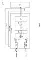
- FIG. 1 is a block diagram of a system 100 employing the present invention.
- system 100 is a router, although the present invention can be employed in any network device utilized in the transfer of data in a network (e.g ., a switch, a network storage processing device, etc).
- System 100 includes a number of ( e.g ., N) line cards 102, each having similar circuitry and each coupled to a switch fabric 104.
- line card 102 refers to any of line cards 102(1) - 102(N), unless otherwise specified.
- Various hardware and software components associated with system 100 are not shown in order to aid clarity.
- variable identifier "N" is used in Figure 1 (and in other parts of this application) to more simply designate the final element (e.g ., line card 102 (N)) of a series of related or similar elements.
- the repeated use of such variable identifiers is not meant to imply a correlation between the sizes of such series of elements, although such correlation may exist.
- the use of such variable identifiers does not require that each series of elements has the same number of elements as another series delimited by the same variable identifier. Rather, in each instance of use, the variable identified by "N" may hold the same or a different value than other instances of the same variable identifier.
- line card 102 transmits and receives data streams to and from clients (not shown) of a local network (not shown) over communication lines 106.
- communication lines 106 carry packets in accordance with the 10 Gigabit Ethernet (GbE) protocol.
- the incoming packets provided on communication lines 106 are received by ports 108 of line card 102. From ports 108, the packets are transferred to a link aggregation device 110 via an interface 112. From link aggregation device 110, packets are transferred to a network processor 114 and a fabric interface 116 via interfaces 118 and 120 respectively. Generally, fabric interface 116 converts a stream of data from one format (e.g. , packets) to another (e.g ., common switch interface cells). From fabric interface 116 the packets are transferred to switch fabric 104. In similar fashion, the packets are transferred from switch fabric 104 to client devices along an opposite path through system 100.
- a link aggregation device 110 From link aggregation device 110, packets are transferred to a network processor 114 and a fabric interface 116 via interfaces 118 and 120 respectively.
- fabric interface 116 converts a stream of data from one format (e.g. , packets) to another (e.g ., common switch interface cells). From
- interfaces 112, 118, and 120 should provide high data transfer rates for the packets transferred between the respective integrated circuits. Accordingly, in one embodiment of the present invention, interfaces 112, 118, and 120 enable packets to be transferred between integrated circuits at a data rate of approximately 20Gbs ( e.g ., between 19Gbps and 38Gbps).
- interfaces 112, 118, 120 are compatible with existing interfaces, for example the System Packet Interface Level 4 Phase 2 (SPI-4.2) interface. Devices configured to operate in accordance with the interface of the present invention are compatible with, and may transfer data between, devices configured with the SPI-4.2 interface and interfaces similar thereto. It is noted that the system and integrated circuits of Figure 1 provide only an exemplary context in which to describe the present invention. The present invention is not limited to interfacing the integrated circuits of Figure 1 , but can be used to interface other devices which are utilized in the transfer of network data.
- SPI-4.2 System Packet Interface Level 4 Phase 2
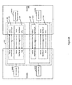
- FIG. 2A is a block diagram illustrating an interface according to one embodiment of the present invention.
- interface 200 enables data to be transferred between a device A 202 and a device B 204 at high data rates (e.g ., approximately equal to 20 Gbps).
- device 202 and device 204 operate at different layers of the OSI reference model.
- device 202 may be a physical layer device (e.g ., SONET framer, Ethernet MAC, and the like) and device 204 may be a network layer device (e.g ., network processors, and other such devices).
- Interface 200 includes a transmit interface 206 and a receive interface 208.
- Transmit interface 206 includes a transmit data bus 210 and a transmit status bus 212.
- Receive interface 208 includes a receive data bus 214 and a receive status bus 216.
- Transmit data bus 210 and receive data bus 214 are unidirectional data busses configured to transfer data in opposite directions from each other.
- Transmit interface 206 and receive interface 208 include out-of-band status information for each respective device 202 and 204 so that the FIFOs of the each receiving device may be more efficiently utilized.
- a receiving device (or a sink) is used to refer to a device configured to receive data on a data bus in accordance with the present invention
- a transmitting device (or a source) is used to refer to a device configured to transmit data on a data bus in accordance with the present invention
- a single device can be both a receiving device and a transmitting device
- device 202 is a receiving device with respect to transmit interface 206, but is a transmitting device with respect to receiving interface 208.
- device 204 is a receiving device with respect to receive interface 208, but is a transmitting device with respect to transmit interface 206.
- transmit data bus 210, transmit status bus 212, receive data bus 214 and receive status bus 216 use low-voltage differential signaling (LVDS) as defined in IEEE 1596.3-1996. However other comparable signaling techniques maybe used.
- LVDS low-voltage differential signaling
- Transmit data bus 210 includes two transmit data clock signals (TDCLK1 and TDCLK2), 32 data signals (TDAT[15:0] and TDAT[31:16]), and a single transmit control signal (TCTL).
- Transmit status bus 212 includes a transmit status clock signal (TSCLK) and two transmit status signals (TSTAT[1:0]).
- receive data bus 214 includes two transmit data clock signals (RDCLK1 and RDCLK2), 32 data signals (RDAT[15:0] and RDAT[31:16]) and a single control signal (RCTL).
- Receive status bus 216 includes receive status clock signal (RSCLK) and two receive status signals (RSTAT[1:0]).
- Transmit interface 206 and receive interface 208 are coupled to controllers 218 and 220, respectively. Controllers 218 and 220 contain configuration information for each interface and also operate to control each interface. Transmit interface 206 and receive interface 208 operate independently from each other. Both interfaces are equivalent to each other except that each transfers data and status in opposite directions. Accordingly, to aid clarity while providing brevity, reference will be made to the signals of each interface irrespective of whether they are part of transmit interface 206 or receive interface 208. For example, SCLK will be used to refer to both TSCLK and RSCLK, DAT[15:0] will refer to both TDAT[15:0] and RDAT[15:0], and so on.
- interface 200 utilizes clock-forwarding.
- clock-forwarding By using clock-forwarding, separate clock signals are provided on each bus rather than embedding the clock signals in other signals. This saves the receiving device the burden of having to recover the clock signal.
- DCLK1 and DCLK2 utilize source-synchronous, double-edge clocking at a rate of 311 MHz. Double-edge clocking at a rate of 311Mhz is equivalent to a data rate of 622 Mbps per signal. Since DAT[31:0] includes 32 data signals, an interface according to the present invention provides a data rate of 622 Mbps * 32 or approximately 20Gbs.
- data on DAT[31:0] can be aligned with a clock signal either statically or dynamically.
- static alignment the phase relationship between the data bits and their corresponding clock must be tightly controlled.
- dynamic alignment the receiver compensates for the phase difference between the clock and the individual data bits. It is preferable to use dynamic alignment when the signal path length and/or the frequency of operation create significant skew between the clock and the data.
- DCLK2 is used to sample DAT[31:16] and DCLK1 is used to sample DAT[15:0] and CTL.
- DCLK1 and DCLK2 are in phase with each other.
- dynamic alignment it is preferable that DCLK1 be used to sample DAT[31:0] and CTL.
- DCLK2 may be tri-stated.
- Data words and in-band control words are transferred between device 202 and 204 on DAT[31:0].
- an "in-band" signal describes a signal that is transferred over the same communication lines as another signal.
- a word is 32 bits.
- a data word refers to 32 bits of packet data (including some or all of header information, payload data, trailer information, padding, etc.)
- a control word refers to 32 bits of control information, parity information, and other information.
- a word (either a control word or a data word) is transferred on DAT [31:0] in two portions, an upper portion and a lower portion.
- DAT[15:0] is used to transfer the lower 16 bits of a word and DAT[31:16] is used to transfer the upper 16 bits of the word.
- the data transmit procedure and a description of exemplary control information is provided below.
- a single control signal, CTL is used to distinguish data words and control words on DAT[31:0].
- CTL accompanies each transfer on DAT[31:0].
- CTL is driven off of the rising and the falling edges of CLK1 because data is transferred on both the rising and falling edges of CLK1.
- CTL transitions high (e.g ., a logic 1) to signal that a control word is present on DAT[31:0].
- CTL remains low ( e.g ., a logic 0) otherwise.
- the use of a single control line provides compatibility between the interface of the present invention and other interfaces (e.g ., the data rate of control words transmitted on the present invention is compatible with the SPI-4.2 interface).
- the use of a single control line to identify control words on DAT[31:0] reduces the complexity of a receiving device. For example, with a single control line, a receiving device need only process a single control word in one bit time.
- interface 200 In addition to providing an interface to transfer data and control words at a rate of approximately 20Gbps, interface 200 also provides for the transfer of status information independently from the transfer of data and control words.
- transmit status bus 212 includes TSTAT[1:0] and TSCLK.
- receive status bus 216 includes RSTAT[1:0] and RSCLK.
- STAT[1:0] provides downstream queue information from a receiving device to a transmitting device.
- STAT[1:0] transfers first-in first-out queue (FIFO) status information, error detection and framing information and is clocked by SCLK.
- the data rate of the status is 1/8 th the data rate of the data bus.
- FIG. 2B illustrates an alternative embodiment of the present invention.
- Interface 250 is similar to interface 200 except that a single clock, DCLK, is provided for each interface.
- DCLK a single clock
- One advantage that the embodiment illustrated in Figure 2A provides over the embodiment illustrated in Figure 2B is that a bit-deskew circuit is not required. Because the embodiment shown in Figure 2A generally requires that data signal traces be closely matched, associating fewer signals with a clock signal makes it easier to align the signals. For example, by providing two clock signals, DCLK1 and DCLK2, for DAT[15:0] and DAT[31:16], respectively, DCLK1 and DCLK2 will be less affected by jitter, noise and other impacts associated with circuit design. Thus, the constraints on the routing of the signals between two devices interfaced with the present invention can be relaxed.
- Control word 300 is 32 bits wide and is used to identify, among other things, a start of packet, an end of packet, and a port address for packets transferred on DAT[31:0].
- control word 300 includes a parity field (DIP-4) 302, a port address field (ADR) 304, a start-of packet (SOP) field 306, an end-of-packet (EOP) status field 308, a type field 310, an extended parity field 312, a reserved field 314, and an extended EOP status field 316.
- DIP-4 parity field
- ADR port address field
- SOP start-of packet
- EOP end-of-packet
- type field 310 an extended parity field 312, a reserved field 314, and an extended EOP status field 316.
- Parity field 302 and extended parity field 312 provide parity over the control word and the immediately preceding data words.
- Parity field 302 is computed over the lower portion of the control word transferred on DAT[15:0] and also the immediately preceding 16 bits of the data words transferred on DAT[15:0] following the last control word.
- Extended parity field 312 is computed over the upper portion of the control word transferred on DAT[31:16] and also the immediately preceding 16 bits of the data words transferred on DAT[31:16] following the last control word.
- the parity is a 4-bit Diagonal Interleaved Parity (DIP-4) as described in "System Packet Interface Level 4 (SPI-4) Phase 2 : OC-192 System Interface for Physical and Link Layer Devices, Optical Internetworking Forum Implementation Agreement, January 2001".
- DIP-4 Diagonal Interleaved Parity
- Port address field 304 is the 8-bit port address of the data word immediately following the control word. While the presently described embodiment supports 256 port addresses, other embodiments can support more port addresses, by increasing the size port address field 304 and/or by use of address extension for example.
- Start-of-packet field 306 identifies whether the data immediately following the control word is the start of a packet.
- SOP field 306 is set to 1 to identify a start of packet.
- EOPS field 308 and EOPS_EX field 316 identify the status of the data immediately preceding the control word and are also used to locate the last byte of the packet. Table 1 below provides the values of EOP status field 308 and EOPS_EX field 316 along with the corresponding meaning for each.
- Data words, control words, and training sequences can be transferred on the data bus.
- the present invention utilizes a single control line, CTL, to signal when control words are present on DAT[31:0]. In one embodiment, when the control line is high, control words are present on DAT[31:0]. In one embodiment of the present invention, the upper portion of the control word (i.e ., bits 31- 16) is transferred on DAT[31:16] and, in the same cycle, the lower portion of the control word ( i.e ., bits 15 - 0) is transferred on DAT[15:0].
- Data is transferred on DAT[31:0] in bursts that have a programmable maximum length (referred to as MaxBurst1 or MaxBurst2). It is preferable that the burst length be a multiple of 32 bytes or, if not a multiple of 32 bytes, be terminated with an EOP control word.
- Complete packets can be transferred in a single burst, or broken up into multiple bursts with the transfer of other packets in between. Once a burst transfer has begun, data words are sent uninterrupted until an EOP control word is received or a multiple of 32 bytes has been reached.
- Table 2 identifies the order in which data words are transferred over DAT[31:0], according to one embodiment of the present invention.
- Figure 4 illustrates a state diagram 400 showing the various states of the present invention and the transitions there between.
- Figure 4 is described with reference to the signals illustrated in Figure 2 .
- the data bus of an interface in accordance with the present invention comprises five states: idle control state 402, data burst state 404, training data state 406, training control state 408, and payload control state 410.
- the data bus e.g ., DAT[31:0]
- DAT[31:0] is configured to transfer idle control words, payload control words, data words, training control words, or training data words.
- state diagram 400 will be described with the data bus initially in idle control state 402.
- a data bus in idle state 402 is configured to transfer an idle control word in the current cycle.
- the data bus can remain resident in idle control state 402 (represented by transition 436) and continue transferring idle control words. From idle control state 402, the data bus can transition to payload control state 410 (via transition 432) to begin a data burst or the data bus can transition to training control state 408 (via transition 430) to initiate a training sequence.
- Payload control state 410 signals the beginning of a data burst.
- a data burst refers to an uninterrupted transfer of data words on DAT[31:0].
- a data burst terminates when either MaxBurst1 or MaxBurst2 (described above with reference to Figure 3 ) have been satisfied or when the next control word is received.
- a data bus in payload control state 410 then transitions to data burst state 404 via transition 412. In one embodiment of the present invention, the transition occurs immediately on the clock cycle following the transfer of the SOP control word.
- data burst state 404 data words are transferred over DAT[31:0] in bursts (uninterrupted transfers). As noted above, a data burst occurs on the next immediate clock cycle following the control word. Once a data burst transfer has begun, residence in data burst state 404 is maintained and data words continue to be sent over DAT[31:0] (represented by transition 416) until either an EOP control word is sent or an allowed number of 32-byte blocks has been reached. It is preferable that the maximum configured payload data transfer size be a multiple of 32 bytes or otherwise be terminated by and EOP control word.
- the data bus can transition to idle control state 402 (via transition 434) or the data bus can return to payload control state 410 (via transition 414) to send a new SOP control word to begin another data burst, or any other control word can be sent (e.g ., an SOP for another channel).
- successive SOP control words should occur not less than 8 clock cycles apart.
- a cycle as used herein, is defined as one control or data word (and because embodiments of the present invention utilize DDR, clock cycles as used herein can refer to DDR clock cycles and non-DDR clock cycles). Consequently, a data burst lasting less than 8 cycles could be filled with enough idle control words so that 8 cycles have passed since an SOP control word was last sent. For example, this can be accomplished by transitioning from data burst state 404 to idle control state 402 via transition 434 and sending at least enough idle control words to reach 8 cycles since the last SOP control word.
- a short data burst i.e ., an EOP burst
- another short data burst i.e ., an EOP burst
- the data path can transition to payload control state 410 to send a new SOP control word to initiate the new data burst.
- a payload control word that separates two adjacent burst transfers contains status information pertaining to the previous transfer and the subsequent transfer.
- a training sequence can be used by a receiving device for deskewing bit arrival times on DAT[31:0], and also deskewing the CTL signal with DAT[31:0].
- the training sequence is intended to allow the receiving device to correct relative skew differences up to +/- 1 bit time.
- the training sequence consists of 1 idle control word followed by one or more repetitions of a 20-word training pattern.
- a training pattern consists of 10 repeated training control words followed by 10 repeated data words.
- the initial idle control word is sent prior to the initial training control word in order to remove dependencies of the parity in the training control words from any preceding data words.
- the training control word is orthogonal to the training data word.
- the training sequence be provided every DATA_MAX_T cycles, where DATA_MAX_T cycles is a programmable value. Additionally, it is preferable that the training pattern be repeated alpha ( ⁇ ) times every DATA_MAX_T cycles.
- Table 3 illustrates a training pattern utilized by one embodiment of the present invention.
- X, efgh, Y and abcd depend on the contents of the interval after the last preceding control word. For example, X and Y reflect whether the preceding data burst was an end of packet or the start of the next packet.
- the values of a, b, c, d, e, f, g, h depend on the parity of the preceding data.
- training control state 408 is entered into from idle control state 402 by sending a training control word. After having transitioned to training control state 408, nine additional training control words are provided on DAT[31:0] making for a total of 10 training control words sent. Following the transfer of 10 training control words, the data bus transitions to training data state 406 to provide 10 repeated training data words. The transition between training control state 408 and training data state 406 is repeated until the bits transferred to the receiving device have been sufficiently deskewed.
- a training sequence is first initiated (e.g ., at startup of a receiving and transmitting device), the training sequence should be repeated until the receiving device stops transmitting a framing pattern via the status bus.
- synchronization of the signals can be determined by the detection of consecutive sequences having matching parity (i.e ., consecutive DIP-4) matches.
- alpha ( ⁇ ) determines the number of repetitions.
- the transmitting device When periodic training is performed (as opposed to training at startup), the transmitting device should schedule the training sequence at least every DATA_MAX_T clock cycles. In addition, the training pattern should then be repeated alpha ( ⁇ ) times.
- DATA_MAX_T and ⁇ are both configurable values, and training sequences for each interface, receiving and transmitting, may be scheduled independently. It is preferable for the transmitting device to wait for the completion of the current data burst before starting the transmission of the training sequence and not interrupt a data burst with a training sequence.
- Figure 5 illustrates a timing diagram in which data can be aligned using static alignment. Because static alignment generally requires that data signal traces be closely matched, associating fewer signals with a clock signal makes it easier to align the signals. Thus, by using two clock signals rather than one clock signal for 32 bits of data, the number of data signals matched to each clock is limited to 16. In static alignment, the data and the clock are transmitted to the receiver in a fixed phase relationship utilizing both DCLK1 and DCLK2. The lower 16 bits (bits 15-0) of control and data words are transferred on DAT[15:0] while the upper 16 bits (bits 31:15) of control and data words are transferred on DAT[31:15].
- DAT[15:0] and CTL be matched within +/-2 bit times to DAT[31:16].
- DAT[15:0] and DAT[31:16] "match" when the variation in the propagation time between the transmitting device and the receiving device, and between DAT[15:0] and DAT[31:16] is less than two bit times.
- DCLK1 is used to sample DAT[15:0] and CTL while DCLK2 is used to sample DAT[31:16].
- the receiving device should re-align DAT[31:16] and DAT[15:0] to a single clock.
- the alignment by the receiving device is done using the training sequence at start-up and the word alignment circuit of Figure 6 (where start-up is defined as the point at which the devices are powered on and initialized).
- Figure 6A illustrates an example word alignment circuit which can be utilized to deskew a number of communication lines with respect to each other.
- a source 600 provides CLK1 and CLK2 to a sink 602.
- Sink 602 includes front end circuits 604 and 606.
- Front end circuit 604 receives CTL, DAT[15:0] and CLK1 and samples CTL and DAT[15:0] with CLK1.
- front end circuit 606 receives CLK2 and DAT[31:16] and samples DAT[31:16] with CLK2. Because DAT[15:0] can be skewed from DAT[31:16], it is necessary to deskew the groups of signals with respect to each other.
- the present invention provides word alignment circuit 608 which receives DAT[15:0], CTL, and DAT[31:16] and deskews these signals with respect to each other.
- Figure 6B illustrates one embodiment of a word alignment circuit 608.
- Word alignment circuit 608 includes data registers 610 multiplexers 612 and 614, a control circuit 616 and a data register 618.
- Data registers 610 provide delayed "versions" of DAT[31:0] and CTL to multiplexers 612 and 614. For example, DART[15:0] and CTL are provided to multiplexer 612 on signal 620(a) without any delay. DAT[15:0] and CTL are delayed by data register 610(a) and provided to multiplexer 612 on signal 620(b). DAT[15:0] and CTL are delayed by both data registers 610(a) and 610(b) and provided to multiplexer 612 on signal 620(c).
- Control 616 is coupled to the select lines of multiplexer 612 and 614 and is configured to a version of DAT[15:0] and CLT from multiplexer 612 that matches with a version of DAT[31:16] from multiplexer 614. For example, if a middle phase of DAT[15:0] and CTL (provided on data signal 620(b)) matches a late phase of DAT[31:16] (provided on signal 622(c)), control 616 selects signal 620(b) from multiplexer 612 and signal 622(c) from multiplexer 614. So that control 616 selects the signals at the appropriate time to align the outputs from each multiplexer 612 and 614 with each other, control 616 is set during the training sequence provided at start-up.
- Figure 7 illustrates a timing diagram in which data is aligned using dynamic alignment.
- bits DAT[31:0] and CTL are not aligned with respect to DCLK1. It is preferable to use dynamic alignment when the signal path length and/or the frequency of operation create significant skew between clock and data.
- the source device tri-states the additional clock signal (e.g ., DCLK2). As shown in Figure 7 , control words and data words are transferred on DAT[31:0] with every rising and falling edge of CLK1.
- the upper portion (i.e ., bits 31:16) of the data words and control words are provided on DAT[31:16] and the lower portion (i.e., bits 15:0) re provided on DAT[15:0].
- a single control line is used to distinguish data words from control words on DAT[31:0].
- CTL is high when a control word is on DAT[31:0].
- Figure 8 illustrates clocking with dynamic alignment for an interface in accordance with one embodiment of the present invention.
- a source 802 provides CTL, DAT[31:0], and DCLK1 signals to sink 804.
- Sink 804 provides STAT[1:0] and SCLK signals to source 802.
- Sink 804 includes a bit deskew circuit 806 and a word alignment circuit 808.
- bit deskew circuit samples DAT[31:0] and CLK with respect to the clock signal to locate a window in which data transitions of the signals are occurring and then determines a sample point centered in the window.
- Word alignment circuit 808 detects the training pattern provided by source 802 and uses a known version of the training pattern to adjust alignment of the bits of data so they are aligned within the word.
- An interface in accordance with the present invention enables a receiving device storing the data words in queues (not shown) to transmit queue status to the transmitting device.
- the transfer of fifo status allows for, among other advantages, the efficient transfer of data words over the interface of the present invention.
- Figure 9 is a state diagram 900 illustrating how status is provided from a receiving device to a transmitting device over a status bus in accordance with the present invention (e.g ., transmit status bus 212 or receive status bus 216).
- the status bus is in disable state 902 and configured to send a "1 1" over STAT[1:0] ( i.e ., transmits a 1 on STAT[1] and a 1 on STAT[0]).
- the status bus transitions to sync state 906 via transition 908.
- FIFO status transmission can be enabled by a control processor (not shown) that is initializing a receiving device and a transmitting device.
- a receiving device transfers a framing pattern over STAT[1:0].
- a "11" is transferred over STAT[1:0] as the framing pattern.
- the transfer of a framing pattern transitions the status bus from sync state 906 to fifo status state 910 via transition 912.
- fifo status state 910 the receiving device sends the fifo status to the transmitting device.
- the fifo status may be one of three values: "SATISFIED", "HUNGRY”, and "STARVING".
- a status of "SATISFIED” is indicated by the presence of"1 0" on STAT[1:0]
- "HUNGRY” is indicated by the presence of” 0 1" on STAT[1:0]
- "STARVING" is indicated by "0 0" on STAT[1:0].
- the status of "HUNGRY” indicates to a transmitting device that the transmitting device can transfer up to MaxBurst2 32-byte blocks to the corresponding port until the next status update is provided.
- the corresponding port was previously granted a value larger than 32-byte blocks (e.g ., MaxBurst1) which have not been used, the greater value of 32-byte blocks can be transferred to the HUNGRY port.
- the status of "STARVING" signals that the transmitting device can transfer up to MaxBurst1 32-byte blocks to the corresponding port until the next status update.
- the status of "SATISFIED” signals that a transmitting device can only transfer the remaining number of 32-byte blocks previously granted to that port until the next status update. Partial 32-byte transfers are treated as a full 32-byte transfer.
- One embodiment of the present invention utilizes a programmable calendar sequence to indicate which status on the status bus corresponds to which port.
- the first status following the framing pattern corresponds to port(1)
- the second status corresponds to port(2)
- the last status corresponding to port(CALENDAR_LEN).
- the sending of the status for calendar entries 1 to CALENDAR_LEN equals one iteration. Sending of the fifo status is complete when a programmable number of iterations have been transferred.
- the status bus transitions to DIP-2 state 914 via transition 916 to send the parity information for the preceding fifo status.
- the parity is a 2-bit Diagonal Interleaved Parity (DIP-2) as described in "System Packet Interface Level 4 (SPI-4) Phase 2 : OC-192 System Interface for Physical and Link Layer Devices, Optical Internetworking Forum Implementation Agreement, January 2001".
- DIP-2 Diagonal Interleaved Parity
- SPI-4 System Packet Interface Level 4
- Figure 10 is a timing diagram showing the sequence of SCLK, STAT[1], and STAT[0] signals.
- the present interface is compatible with the interface described in "System Packet Interface Level 4 (SPI-4) Phase 2: OC-192 System Interface for Physical and Link Layer Devices, January 2001" (the SPI-4.2 interface).
- SPI-4.2 interface System Packet Interface Level 4
- a device employing the present invention can interface directly with a device employing the SPI-4.2 interface, as described below.
- Figure 11 illustrates a device 1100 coupled to a device 1102.
- Device 1102 is configured to support only the SPI-4.2 interface while device 1100 is configured to support an interface according to the present invention (e.g ., interface 200 of Figure 2 ) and in addition is configured to support the SPI-4.2 interface.
- device 1102 can communicate with device 1100 over the SPI-4.2 interface.
- devices 1100 and 1102 are integrated circuits utilized for the transfer of packets within a network device.
- device 1102 can be configured, via controllers 1118(a) and 1120(b), to operate in one of two modes, a normal mode and an enhanced mode.
- controller 1118(a) contains a mode select bit that, when set ( i.e ., set to "1"), configures device 1102 to operate in an enhanced mode, and when cleared ( i.e ., cleared to "0") configures device 1102 to operate in normal mode.
- a normal mode of operation device 1102 functions in compliance with the SPI-4.2 interface. In normal mode, device 1102 tri-states TDAT[31:16], RDAT[31:16], TDCLK2, and RDCLK2. By tri-stating these signals, they are not sent to device 1100.
- device 1102 when in normal mode, device 1102 does not report parity errors for the extended 4-bit diagonal interleaved parity.
- Device 1102 can also be configured to operate in extended mode, via controller 1118(a) and 1120(b).
- the enhanced mode of operation, described above with respect to Figures 1-11 enables device 1102 to transfer data at significantly greater data rates (e.g ., 20Gbs).
Landscapes
- Engineering & Computer Science (AREA)
- Computer Networks & Wireless Communication (AREA)
- Signal Processing (AREA)
- Communication Control (AREA)
- Information Transfer Systems (AREA)
- Data Exchanges In Wide-Area Networks (AREA)
Claims (25)
- Verfahren, das umfasst:Übertragen von Payload-Steuerinformationen (410) zwischen einer ersten integrierten Schaltung (202) und einer zweiten integrierten Schaltung (204) mittels einer Vielzahl von Datenübertragungsleitungen (16);bei dem Taktzyklusübergang, der auf das Übertragen der Payload-Steuerinformationen (410) folgt, Übertragen gepackter Daten (404) zwischen der ersten integrierten Schaltung (202) und der zweiten integrierten Schaltung (204) mittels der Vielzahl von Datenübertragungsleitungen (16), wobei das Übertragen der gepackten Daten mit einer Datenrate zwischen 19 Gbps und 38 Gbps durchgeführt wird; undÜbertragen eines 1-Bit Steuersignals, um zu identifizieren, wann Payload-Steuerinformationen (410) auf allen der Vielzahl von Übertragungsleitungen (16) vorhanden sind.
- Verfahren nach Anspruch 1, das des Weiteren umfasst:Konfigurieren wenigstens einer der ersten integrierten Schaltung (202) und der zweiten integrierten Schaltung (204), um in einem verbesserten Modus zu arbeiten.
- Verfahren nach Anspruch 1, das des Weiteren umfasst:Konfigurieren wenigstens einer der ersten integrierten Schaltung (202) und der zweiten integrierten Schaltung (204), um in wenigstens einem eines normalen Modus und eines verbesserten Modus zu arbeiten, wobei das Übertragen der gepackten Daten (404) in Übereinstimmung mit dem 10 Gigabit Ethernet, GbE, - Protokoll in dem normalen Modus und mit einer Rate zwischen 19 Gbps und 38 Gbps in dem verbesserten Modus durchgeführt wird.
- Verfahren nach Anspruch 1, wobei das Übertragen der Payload-Steuerinformationen (410) umfasst:Übertragen einer Parität für die gepackten Daten (404) und/oder Übertragen einer Portadresse für die gepackten Daten (404) und/oder Übertragen eines erweiterten Endes des Paketstatus und/oder Übertragen einer erweiterten Parität.
- Verfahren nach einem der vorhergehenden Ansprüche, das des Weiteren umfasst:Übertragen des FIFO-Status zwischen der ersten integrierten Schaltung (202) und der zweiten integrierten Schaltung (204) über eine Vielzahl von FIFO-Statusleitungen.
- Verfahren nach Anspruch 5, wobei der FIFO-Status gleichzeitig mit wenigstens einem des Bereitstellens der Payload-Steuerinformationen (410) und des Bursting der gepackten Daten (404) übertragen wird.
- Verfahren nach Anspruch 5 oder 6, das des Weiteren umfasst:Bereitstellen eines Datentaktsignals von der ersten integrierten Schaltung (202) zu der zweiten integrierten Schaltung (204); undBereitstellen eines FIFO-Status-Taktsignals von der ersten integrierten Schaltung (202) zu der zweiten integrierten Schaltung (204).
- Verfahren nach einem der vorhergehenden Ansprüche, das des Weiteren umfasst:Bereitstellen eines Datentaktsignals zwischen der ersten integrierten Schaltung (202) und der zweiten integrierten Schaltung (204), um die Payload-Steuerinformationen (410) und die gepackten Daten (404) zu takten, wobei der Datentakt eine Minimalfrequenz von 311 MHz hat; undTakten der Payload-Steuerinformationen (410) und der gepackten Daten (404) sowohl an einer steigenden Flanke als auch an einer fallenden Flanke des Datentaktsignals.
- Verfahren nach einem der vorhergehenden Ansprüche, das des Weiteren umfasst:dynamisches Angleichen der gepackten Daten (404) oder statisches Angleichen der gepackten Daten (404).
- Verfahren nach einem der vorhergehenden Ansprüche, das des Weiteren umfasst:Unterweisen der ersten integrierten Schaltung, um die gepackten Daten (404), die auf den Datenübertragungsleitungen (16) übertragen wurden, zu entzerren.
- Verfahren nach Anspruch 10, das des Weiteren umfasst:Übertragen von Unterweisungs-Steuerinformationen (408) zwischen der ersten integrierten Schaltung (202) und der zweiten integrierten Schaltung (204) mittels einer Vielzahl von Datenübertragungsleitungen (16); undbei dem Taktzyklusübergang, der auf das Übertragen der Unterweisungs-Steuerinformationen (408) folgt, Übertragen der Unterweisungsdaten zwischen der ersten integrierten Schaltung (202) und der zweiten integrierten Schaltung (204) mittels der Vielzahl von Datenübertragungsleitungen (16)
- Verfahren nach einem der vorhergehenden Ansprüche, wobei die Payload-Steuerinformationen (410) auf der Vielzahl von Datenübertragungsleitungen (16) vorhanden sind, wenn das 1-Bit Steuersignal eine logische 1 ist.
- Verfahren nach Anspruch 1, das des Weiteren umfasst:Bereitstellen eines ersten Datentaktsignals und eines zweiten Datentaktsignals zwischen der ersten integrierten Schaltung (202) und der zweiten integrierten Schaltung (204), wobei das erste Datentaktsignal den ersten sechzehn Datenübertragungsleitungen der Vielzahl von Datenübertragungsleitungen (16) und das zweite Datentaktsignal den zweiten sechzehn Datenübertragungsleitungen der Vielzahl von Datenübertragungsleitungen (16) entspricht, und wobei die ersten und zweiten Datentaktsignale eine Minimalfrequenz von 311 MHz haben;Takten der Payload-Steuerinformationen (410) und der gepackten Daten (404) sowohl an der steigenden Flanke als auch an der fallenden Flanke der Datentaktsignale.
- Verfahren nach Anspruch 13, das des Weiteren das Neuangleichen der ersten sechzehn Datenübertragungsleitungen der Vielzahl von Datenübertragungsleitungen (16) mit den zweiten sechzehn Datenübertragungsleitungen der Vielzahl von Datenübertragungsleitungen (16) umfasst.
- Verfahren nach Anspruch 9, wobei das statistische Angleichen umfasst:Fordern, dass die ersten sechzehn Datenübertragungsleitungen der Vielzahl von Datenübertragungsleitungen (16) und die zweiten sechzehn Datenübertragungsleitungen der Vielzahl von Datenübertragungsleitungen (16) innerhalb von 2 Bitzeiten angepasst werden.
- Verfahren nach Anspruch 1, das des Weiteren umfasst:Bereitstellen von drei Phasen von Daten, die auf den ersten 16 getragen werden, wobei jede der drei Phasen um einen unterschiedlichen Betrag verzögert ist;Bereitstellen von drei Phasen von Daten, die auf den zweiten 16 getragen werden, wobei jede der drei Phasen um einen unterschiedlichen Betrag verzögert ist;Bereitstellen eines Steuersignals, um eine der drei Phasen der ersten 16 an eine der drei Phasen der zweiten 16 anzupassen.
- Verfahren nach Anspruch 9, wobei das dynamische Angleichen des Weiteren umfasst:Abtasten der Vielzahl von Datenübertragungsleitungen (16), wobei das Abtasten das Bestimmen umfasst, welche der Vielzahl von Datenübertragungsleitungen während eines Zeitfensters einen Übergang vollzieht;Auswählen eines Abtastpunkts innerhalb des Zeitfensters;Ermitteln eines Unterweisungsmusters, wobei das Ermitteln mittels einer Bitentzerrungsschaltung durchgeführt wird; undVerwenden des Unterweisungsmusters, um die Vielzahl von Datenübertragungsleitungen auszurichten.
- Vorrichtung, die aufweist:eine Einrichtung zum Bereitstellen von Payload-Steuerinformationen (410);bei dem Taktzyklusübergang, der auf das Übertragen der Payload-Steuerinformationen (410) folgt, eine Einrichtung zum Bereitstellen gepackter Daten (404) mit einer Datenrate zwischen 19 Gbps und 38 Gbps;eine Einrichtung zum Identifizierten, ob die Daten Payload-Steuerinformationen (410) oder gepackte Daten (404) sind;eine Einrichtung zum Empfangen von Payload-Steuerinformationen (410); undbei dem Taktzyklusübergang, der auf das Empfangen der Payload-Steuerinformationen (410) folgt, eine Einrichtung zum Empfangen gepackter Daten (404) mit einer Datenrate zwischen 19 Gbps und 38 Gbps, und wobei die Einrichtung zum Empfangen gepackter Daten (404) unabhängig von der Einrichtung zum Bereitstellen der gepackten Daten (404) arbeitet.
- Vorrichtung nach Anspruch 18, die aufweist:einen Übertragungsdatenbus, der so konfiguriert ist, dass er
die Payload-Steuerinformationen (410) überträgt; und
bei dem Taktzyklusübergang, der auf das Übertragen der Payload-Steuerinformationen (410) folgt, gepackte Daten (404) überträgt, wobei die Übertragung der gepackten Daten (404) mit einer Datenrate zwischen 19 Gbps und 38 Gbps erfolgt;ein 1-Bit Übertragungssteuersignal, um zu identifizieren, ob Daten auf dem Übertragungsdatenbus Payload-Steuerinformationen (410) oder gepackte Daten (404) sind;einen Empfangsdatenbus, der so konfiguriert ist, dass er
die Payload-Steuerinformationen (410) empfängt; und
bei dem Taktzyklusübergang, der auf das Empfangen der Payload-Steuerinformationen (410) folgt, gepackte Daten (404) empfängt, wobei die gepackten Daten (404) mit einer Datenrate zwischen 19 Gbps und 38 Gbps empfangen werden, und wobei der Empfangsdatenbus unabhängig von dem Übertragungsdatenbus arbeitet; undein 1-Bit Empfangssteuersignal, um zu identifizieren, ob Daten auf dem Empfangsdatenbus Payload-Steuerinformationen (410) oder gepackte Daten (404) sind. - Vorrichtung nach Anspruch 18 oder 19, wobei die Einrichtung zum Bereitstellen der gepackten Daten (404) aufweist:ein erstes und ein zweites Übertragungsdatentaktsignal; undwenigstens 32 Übertragungsdatensignale.
- Vorrichtung nach einem der Ansprüche 18 bis 20, die des Weiteren aufweist:eine Einrichtung zum Betreiben der Einrichtung zum Bereitstellen der gepackten Daten (404) und der Einrichtung zum Empfangen der gepackten Daten (404) in einem verbesserten Modus und einem normalen Modus, wobei die Datenrate der Schnittstelle in dem verbesserten Modus annähernd gleich dem Zweifachen der Datenrate der Schnittstelle in dem normalen Modus ist.
- Vorrichtung nach einem der Ansprüche 18 bis 21, wobei
die Einrichtung zum Bereitstellen von Payload-Steuerinformationen (410) und gepackter Daten eine erste integrierte Schaltung aufweist, und die Einrichtung zum Empfangen von Payload-Steuerinformationen (410) und gepackter Daten eine zweite integrierte Schaltung (204) aufweist;
wobei die Vorrichtung des Weiteren aufweist:eine Einrichtung zum Übertragen von Payload-Steuerinformationen (404) zwischen der ersten integrierten Schaltung (202) und der zweiten integrierten Schaltung (204);eine Einrichtung zum Übertragen gepackter Daten (404) zwischen der ersten integrierten Schaltung (202) und der zweiten integrierten Schaltung (204) mittels einer Vielzahl von Datenübertragungsleitungen (16), wobei die Einrichtung zum Übertragen der gepackten Daten (404) mit einer Datenrate zwischen 19 Gbps und 38 Gbps betreibbar ist; undeine Einrichtung zum Übertragen eines 1-Bit Steuersignals, um zu identifizieren, wann Payload-Steuerinformationen (410) auf allen der Vielzahl von Datenübertragungsleitungen (16) vorhanden sind. - Vorrichtung nach Anspruch 22, die des Weiteren aufweist:eine Einrichtung zum Konfigurieren wenigstens einer der ersten integrierten Schaltung (202) und der zweiten integrierten Schaltung (204), um in wenigstens einem eines normalen Modus und eines verbesserten Modus zu arbeiten, wobei die Einrichtung zum Übertragen der gepackten Daten (404) in Übereinstimmung mit dem 10 Gigabit Ethernet, GbE, - Protokoll in dem normalen Modus und zwischen 19 Gbps und 38 Gbps in dem verbesserten Modus betrieben wird.
- Vorrichtung nach Anspruch 22 oder 23, die des Weiteren aufweist:eine Einrichtung zum Übertragen des FIFO-Status zwischen der ersten integrierten Schaltung (202) und der zweiten integrierten Schaltung (204) über eine Vielzahl von FIFO-Statusleitungen.
- Vorrichtung nach einem der Ansprüche 20 bis 24, die des Weiteren aufweist:eine Einrichtung zum dynamischen Angleichen der gepackten Daten (404) oder eine Einrichtung zum statischen Angleichen der gepackten Daten (404).
Applications Claiming Priority (2)
| Application Number | Priority Date | Filing Date | Title |
|---|---|---|---|
| US10/458,357 US7408878B2 (en) | 2003-06-10 | 2003-06-10 | System packet interface |
| PCT/US2004/018871 WO2004112421A1 (en) | 2003-06-10 | 2004-06-10 | System packet interface |
Publications (2)
| Publication Number | Publication Date |
|---|---|
| EP1632103A1 EP1632103A1 (de) | 2006-03-08 |
| EP1632103B1 true EP1632103B1 (de) | 2009-02-11 |
Family
ID=33510566
Family Applications (1)
| Application Number | Title | Priority Date | Filing Date |
|---|---|---|---|
| EP04755185A Expired - Lifetime EP1632103B1 (de) | 2003-06-10 | 2004-06-10 | Paketschnittstellensystem |
Country Status (8)
| Country | Link |
|---|---|
| US (1) | US7408878B2 (de) |
| EP (1) | EP1632103B1 (de) |
| CN (1) | CN1781333B (de) |
| AT (1) | ATE422787T1 (de) |
| AU (1) | AU2004247254B2 (de) |
| CA (1) | CA2521659C (de) |
| DE (1) | DE602004019409D1 (de) |
| WO (1) | WO2004112421A1 (de) |
Families Citing this family (30)
| Publication number | Priority date | Publication date | Assignee | Title |
|---|---|---|---|---|
| US7573896B2 (en) * | 2004-10-15 | 2009-08-11 | Integrated Device Technology, Inc. | Method and apparatus for generic interface, packet cut-through, overbooking, queue concatenation, and logical identification priority for a system packet interface device |
| EP1684164A1 (de) * | 2005-01-13 | 2006-07-26 | Thomson Licensing | Datenübertragungssystem |
| US7401246B2 (en) | 2005-06-30 | 2008-07-15 | Intel Corporation | Nibble de-skew method, apparatus, and system |
| US20070073932A1 (en) * | 2005-09-13 | 2007-03-29 | Alcatel | Method and apparatus for a configurable data path interface |
| JP4651555B2 (ja) * | 2006-02-13 | 2011-03-16 | 富士通株式会社 | フレームバッファ監視方法及び装置 |
| US8165025B2 (en) * | 2006-12-08 | 2012-04-24 | Ixia | Method and apparatus for generating a unique packet identifier |
| US7467056B2 (en) * | 2007-03-09 | 2008-12-16 | Nortel Networks Limited | Method and apparatus for aligning multiple outputs of an FPGA |
| US7865753B2 (en) * | 2007-03-28 | 2011-01-04 | Intel Corporation | Resource power controller to return a resource to an up state based on an estimate of a size of a gap in data traffic |
| US8060681B2 (en) | 2007-11-27 | 2011-11-15 | Microsoft Corporation | Interface protocol and API for a wireless transceiver |
| US8958460B2 (en) | 2008-03-18 | 2015-02-17 | On-Ramp Wireless, Inc. | Forward error correction media access control system |
| US8477830B2 (en) | 2008-03-18 | 2013-07-02 | On-Ramp Wireless, Inc. | Light monitoring system using a random phase multiple access system |
| US20090239550A1 (en) * | 2008-03-18 | 2009-09-24 | Myers Theodore J | Random phase multiple access system with location tracking |
| US7593452B1 (en) | 2008-03-18 | 2009-09-22 | On-Ramp Wireless, Inc. | Despreading spread spectrum data |
| US8520721B2 (en) | 2008-03-18 | 2013-08-27 | On-Ramp Wireless, Inc. | RSSI measurement mechanism in the presence of pulsed jammers |
| US7773664B2 (en) | 2008-03-18 | 2010-08-10 | On-Ramp Wireless, Inc. | Random phase multiple access system with meshing |
| US7733945B2 (en) | 2008-03-18 | 2010-06-08 | On-Ramp Wireless, Inc. | Spread spectrum with doppler optimization |
| US8363699B2 (en) | 2009-03-20 | 2013-01-29 | On-Ramp Wireless, Inc. | Random timing offset determination |
| US7639726B1 (en) | 2009-03-20 | 2009-12-29 | On-Ramp Wireless, Inc. | Downlink communication |
| US7702290B1 (en) | 2009-04-08 | 2010-04-20 | On-Ramp Wirless, Inc. | Dynamic energy control |
| US8565811B2 (en) * | 2009-08-04 | 2013-10-22 | Microsoft Corporation | Software-defined radio using multi-core processor |
| US9753884B2 (en) * | 2009-09-30 | 2017-09-05 | Microsoft Technology Licensing, Llc | Radio-control board for software-defined radio platform |
| US8627189B2 (en) | 2009-12-03 | 2014-01-07 | Microsoft Corporation | High performance digital signal processing in software radios |
| US20110136439A1 (en) * | 2009-12-04 | 2011-06-09 | Microsoft Corporation | Analyzing Wireless Technologies Based On Software-Defined Radio |
| CN103503375B (zh) | 2011-05-04 | 2017-05-03 | 微软技术许可有限责任公司 | 基站频谱分配 |
| US9130711B2 (en) | 2011-11-10 | 2015-09-08 | Microsoft Technology Licensing, Llc | Mapping signals from a virtual frequency band to physical frequency bands |
| US8989286B2 (en) | 2011-11-10 | 2015-03-24 | Microsoft Corporation | Mapping a transmission stream in a virtual baseband to a physical baseband with equalization |
| JP6236945B2 (ja) * | 2013-07-11 | 2017-11-29 | 富士通株式会社 | 伝送装置、伝送システム、及び伝送方法 |
| US9489009B2 (en) * | 2014-02-20 | 2016-11-08 | Samsung Electronics Co., Ltd. | System on chip, bus interface and method of operating the same |
| CN106341340B (zh) * | 2015-07-17 | 2019-10-18 | 深圳市中兴微电子技术有限公司 | 一种报文切片方法及装置 |
| US11558120B1 (en) * | 2021-09-30 | 2023-01-17 | United States Of America As Represented By The Administrator Of Nasa | Method for deskewing FPGA transmitter channels directly driving an optical QPSK modulator |
Family Cites Families (2)
| Publication number | Priority date | Publication date | Assignee | Title |
|---|---|---|---|---|
| GB2259377B (en) * | 1991-08-08 | 1995-06-21 | British Aerospace Space & Comm | Multi-function application specific integrated circuit for controlling spacecraft thrusters |
| WO1998026509A2 (en) * | 1996-11-27 | 1998-06-18 | Dsc Telecom L.P. | Method and apparatus for high-speed data transfer that minimizes conductors |
-
2003
- 2003-06-10 US US10/458,357 patent/US7408878B2/en not_active Expired - Fee Related
-
2004
- 2004-06-10 CN CN2004800111009A patent/CN1781333B/zh not_active Expired - Fee Related
- 2004-06-10 WO PCT/US2004/018871 patent/WO2004112421A1/en not_active Ceased
- 2004-06-10 CA CA2521659A patent/CA2521659C/en not_active Expired - Fee Related
- 2004-06-10 AT AT04755185T patent/ATE422787T1/de not_active IP Right Cessation
- 2004-06-10 EP EP04755185A patent/EP1632103B1/de not_active Expired - Lifetime
- 2004-06-10 DE DE602004019409T patent/DE602004019409D1/de not_active Expired - Lifetime
- 2004-06-10 AU AU2004247254A patent/AU2004247254B2/en not_active Ceased
Also Published As
| Publication number | Publication date |
|---|---|
| US7408878B2 (en) | 2008-08-05 |
| CA2521659C (en) | 2011-01-04 |
| ATE422787T1 (de) | 2009-02-15 |
| EP1632103A1 (de) | 2006-03-08 |
| CA2521659A1 (en) | 2004-12-23 |
| CN1781333B (zh) | 2011-03-30 |
| AU2004247254A1 (en) | 2004-12-23 |
| DE602004019409D1 (de) | 2009-03-26 |
| US20040252684A1 (en) | 2004-12-16 |
| CN1781333A (zh) | 2006-05-31 |
| AU2004247254B2 (en) | 2009-09-10 |
| WO2004112421A1 (en) | 2004-12-23 |
Similar Documents
| Publication | Publication Date | Title |
|---|---|---|
| EP1632103B1 (de) | Paketschnittstellensystem | |
| US6385208B1 (en) | Serial media independent interface | |
| EP1080561B1 (de) | Weiterleitung von paketen mit variabler länge in einem multiport-switch | |
| US8385374B1 (en) | Multilane communication device | |
| US8619781B2 (en) | Backplane interface adapter with error control and redundant fabric | |
| US6798784B2 (en) | Concurrent switching of synchronous and asynchronous traffic | |
| US7519747B1 (en) | Variable latency buffer and method of operation | |
| CN110620809B (zh) | 用于针对有损协议执行包间间隙修复的系统和方法 | |
| US20050207436A1 (en) | Switching device based on aggregation of packets | |
| US6631138B1 (en) | Reduced pin-count 10Base-T MAC to transceiver interface | |
| US6128317A (en) | Transmitter and receiver supporting differing speed codecs over single links | |
| US20040078494A1 (en) | System and apparatus for implementing devices interfacing higher speed networks using lower speed network components | |
| EP1484874B1 (de) | System zum Anschluss eines Media-Access-Control (MAC) Moduls an ein Small-Form-Factor-Pluggable (SFP) Modul | |
| US7535844B1 (en) | Method and apparatus for digital signal communication | |
| US7728625B1 (en) | Serial interface for programmable logic devices | |
| US7149186B1 (en) | Apparatus and method for rate adaptation control | |
| WO2018196833A1 (zh) | 报文发送方法和报文接收方法及装置 | |
| US6611538B1 (en) | Data transmission synchronization system | |
| US6826187B1 (en) | Interfacing between a physical layer and a bus | |
| EP1315397B1 (de) | Sequenzierter Hochgeschwindigkeitsmehrkanalbus | |
| US20040015617A1 (en) | Flexible network interfaces and flexible data clocking | |
| EP1424871B1 (de) | Verfahren und Apparat zur Übertragung sehr hoher Datenraten über eine Zwischen- oder Rückwandleiterplatte | |
| US7519728B1 (en) | Merge systems and methods for transmit systems interfaces | |
| US9048889B1 (en) | High-speed data communications architecture | |
| US20070047579A1 (en) | Multipacket interface |
Legal Events
| Date | Code | Title | Description |
|---|---|---|---|
| PUAI | Public reference made under article 153(3) epc to a published international application that has entered the european phase |
Free format text: ORIGINAL CODE: 0009012 |
|
| 17P | Request for examination filed |
Effective date: 20051130 |
|
| AK | Designated contracting states |
Kind code of ref document: A1 Designated state(s): AT BE BG CH CY CZ DE DK EE ES FI FR GB GR HU IE IT LI LU MC NL PL PT RO SE SI SK TR |
|
| DAX | Request for extension of the european patent (deleted) | ||
| GRAP | Despatch of communication of intention to grant a patent |
Free format text: ORIGINAL CODE: EPIDOSNIGR1 |
|
| GRAS | Grant fee paid |
Free format text: ORIGINAL CODE: EPIDOSNIGR3 |
|
| GRAA | (expected) grant |
Free format text: ORIGINAL CODE: 0009210 |
|
| AK | Designated contracting states |
Kind code of ref document: B1 Designated state(s): AT BE BG CH CY CZ DE DK EE ES FI FR GB GR HU IE IT LI LU MC NL PL PT RO SE SI SK TR |
|
| REG | Reference to a national code |
Ref country code: GB Ref legal event code: FG4D |
|
| REG | Reference to a national code |
Ref country code: CH Ref legal event code: EP |
|
| REG | Reference to a national code |
Ref country code: IE Ref legal event code: FG4D |
|
| REF | Corresponds to: |
Ref document number: 602004019409 Country of ref document: DE Date of ref document: 20090326 Kind code of ref document: P |
|
| PG25 | Lapsed in a contracting state [announced via postgrant information from national office to epo] |
Ref country code: FI Free format text: LAPSE BECAUSE OF FAILURE TO SUBMIT A TRANSLATION OF THE DESCRIPTION OR TO PAY THE FEE WITHIN THE PRESCRIBED TIME-LIMIT Effective date: 20090211 Ref country code: SI Free format text: LAPSE BECAUSE OF FAILURE TO SUBMIT A TRANSLATION OF THE DESCRIPTION OR TO PAY THE FEE WITHIN THE PRESCRIBED TIME-LIMIT Effective date: 20090211 Ref country code: ES Free format text: LAPSE BECAUSE OF FAILURE TO SUBMIT A TRANSLATION OF THE DESCRIPTION OR TO PAY THE FEE WITHIN THE PRESCRIBED TIME-LIMIT Effective date: 20090522 Ref country code: NL Free format text: LAPSE BECAUSE OF FAILURE TO SUBMIT A TRANSLATION OF THE DESCRIPTION OR TO PAY THE FEE WITHIN THE PRESCRIBED TIME-LIMIT Effective date: 20090211 |
|
| NLV1 | Nl: lapsed or annulled due to failure to fulfill the requirements of art. 29p and 29m of the patents act | ||
| PG25 | Lapsed in a contracting state [announced via postgrant information from national office to epo] |
Ref country code: SE Free format text: LAPSE BECAUSE OF FAILURE TO SUBMIT A TRANSLATION OF THE DESCRIPTION OR TO PAY THE FEE WITHIN THE PRESCRIBED TIME-LIMIT Effective date: 20090511 Ref country code: PL Free format text: LAPSE BECAUSE OF FAILURE TO SUBMIT A TRANSLATION OF THE DESCRIPTION OR TO PAY THE FEE WITHIN THE PRESCRIBED TIME-LIMIT Effective date: 20090211 Ref country code: AT Free format text: LAPSE BECAUSE OF FAILURE TO SUBMIT A TRANSLATION OF THE DESCRIPTION OR TO PAY THE FEE WITHIN THE PRESCRIBED TIME-LIMIT Effective date: 20090211 |
|
| PG25 | Lapsed in a contracting state [announced via postgrant information from national office to epo] |
Ref country code: BE Free format text: LAPSE BECAUSE OF FAILURE TO SUBMIT A TRANSLATION OF THE DESCRIPTION OR TO PAY THE FEE WITHIN THE PRESCRIBED TIME-LIMIT Effective date: 20090211 |
|
| PG25 | Lapsed in a contracting state [announced via postgrant information from national office to epo] |
Ref country code: DK Free format text: LAPSE BECAUSE OF FAILURE TO SUBMIT A TRANSLATION OF THE DESCRIPTION OR TO PAY THE FEE WITHIN THE PRESCRIBED TIME-LIMIT Effective date: 20090211 Ref country code: PT Free format text: LAPSE BECAUSE OF FAILURE TO SUBMIT A TRANSLATION OF THE DESCRIPTION OR TO PAY THE FEE WITHIN THE PRESCRIBED TIME-LIMIT Effective date: 20090713 Ref country code: CZ Free format text: LAPSE BECAUSE OF FAILURE TO SUBMIT A TRANSLATION OF THE DESCRIPTION OR TO PAY THE FEE WITHIN THE PRESCRIBED TIME-LIMIT Effective date: 20090211 Ref country code: EE Free format text: LAPSE BECAUSE OF FAILURE TO SUBMIT A TRANSLATION OF THE DESCRIPTION OR TO PAY THE FEE WITHIN THE PRESCRIBED TIME-LIMIT Effective date: 20090211 |
|
| PG25 | Lapsed in a contracting state [announced via postgrant information from national office to epo] |
Ref country code: RO Free format text: LAPSE BECAUSE OF FAILURE TO SUBMIT A TRANSLATION OF THE DESCRIPTION OR TO PAY THE FEE WITHIN THE PRESCRIBED TIME-LIMIT Effective date: 20090211 Ref country code: SK Free format text: LAPSE BECAUSE OF FAILURE TO SUBMIT A TRANSLATION OF THE DESCRIPTION OR TO PAY THE FEE WITHIN THE PRESCRIBED TIME-LIMIT Effective date: 20090211 |
|
| PLBE | No opposition filed within time limit |
Free format text: ORIGINAL CODE: 0009261 |
|
| STAA | Information on the status of an ep patent application or granted ep patent |
Free format text: STATUS: NO OPPOSITION FILED WITHIN TIME LIMIT |
|
| 26N | No opposition filed |
Effective date: 20091112 |
|
| PG25 | Lapsed in a contracting state [announced via postgrant information from national office to epo] |
Ref country code: MC Free format text: LAPSE BECAUSE OF NON-PAYMENT OF DUE FEES Effective date: 20090630 Ref country code: BG Free format text: LAPSE BECAUSE OF FAILURE TO SUBMIT A TRANSLATION OF THE DESCRIPTION OR TO PAY THE FEE WITHIN THE PRESCRIBED TIME-LIMIT Effective date: 20090511 |
|
| REG | Reference to a national code |
Ref country code: CH Ref legal event code: PL |
|
| PG25 | Lapsed in a contracting state [announced via postgrant information from national office to epo] |
Ref country code: IE Free format text: LAPSE BECAUSE OF NON-PAYMENT OF DUE FEES Effective date: 20090610 Ref country code: LI Free format text: LAPSE BECAUSE OF NON-PAYMENT OF DUE FEES Effective date: 20090630 Ref country code: CH Free format text: LAPSE BECAUSE OF NON-PAYMENT OF DUE FEES Effective date: 20090630 |
|
| PG25 | Lapsed in a contracting state [announced via postgrant information from national office to epo] |
Ref country code: GR Free format text: LAPSE BECAUSE OF FAILURE TO SUBMIT A TRANSLATION OF THE DESCRIPTION OR TO PAY THE FEE WITHIN THE PRESCRIBED TIME-LIMIT Effective date: 20090512 |
|
| PG25 | Lapsed in a contracting state [announced via postgrant information from national office to epo] |
Ref country code: IT Free format text: LAPSE BECAUSE OF FAILURE TO SUBMIT A TRANSLATION OF THE DESCRIPTION OR TO PAY THE FEE WITHIN THE PRESCRIBED TIME-LIMIT Effective date: 20090211 |
|
| PG25 | Lapsed in a contracting state [announced via postgrant information from national office to epo] |
Ref country code: LU Free format text: LAPSE BECAUSE OF NON-PAYMENT OF DUE FEES Effective date: 20090610 |
|
| PG25 | Lapsed in a contracting state [announced via postgrant information from national office to epo] |
Ref country code: HU Free format text: LAPSE BECAUSE OF FAILURE TO SUBMIT A TRANSLATION OF THE DESCRIPTION OR TO PAY THE FEE WITHIN THE PRESCRIBED TIME-LIMIT Effective date: 20090812 |
|
| PG25 | Lapsed in a contracting state [announced via postgrant information from national office to epo] |
Ref country code: TR Free format text: LAPSE BECAUSE OF FAILURE TO SUBMIT A TRANSLATION OF THE DESCRIPTION OR TO PAY THE FEE WITHIN THE PRESCRIBED TIME-LIMIT Effective date: 20090211 |
|
| PG25 | Lapsed in a contracting state [announced via postgrant information from national office to epo] |
Ref country code: CY Free format text: LAPSE BECAUSE OF FAILURE TO SUBMIT A TRANSLATION OF THE DESCRIPTION OR TO PAY THE FEE WITHIN THE PRESCRIBED TIME-LIMIT Effective date: 20090211 |
|
| REG | Reference to a national code |
Ref country code: FR Ref legal event code: PLFP Year of fee payment: 12 |
|
| REG | Reference to a national code |
Ref country code: FR Ref legal event code: PLFP Year of fee payment: 13 |
|
| REG | Reference to a national code |
Ref country code: FR Ref legal event code: PLFP Year of fee payment: 14 |
|
| REG | Reference to a national code |
Ref country code: FR Ref legal event code: PLFP Year of fee payment: 15 |
|
| PGFP | Annual fee paid to national office [announced via postgrant information from national office to epo] |
Ref country code: FR Payment date: 20190625 Year of fee payment: 16 |
|
| PGFP | Annual fee paid to national office [announced via postgrant information from national office to epo] |
Ref country code: GB Payment date: 20190627 Year of fee payment: 16 Ref country code: DE Payment date: 20190627 Year of fee payment: 16 |
|
| REG | Reference to a national code |
Ref country code: DE Ref legal event code: R119 Ref document number: 602004019409 Country of ref document: DE |
|
| GBPC | Gb: european patent ceased through non-payment of renewal fee |
Effective date: 20200610 |
|
| PG25 | Lapsed in a contracting state [announced via postgrant information from national office to epo] |
Ref country code: FR Free format text: LAPSE BECAUSE OF NON-PAYMENT OF DUE FEES Effective date: 20200630 Ref country code: GB Free format text: LAPSE BECAUSE OF NON-PAYMENT OF DUE FEES Effective date: 20200610 |
|
| PG25 | Lapsed in a contracting state [announced via postgrant information from national office to epo] |
Ref country code: DE Free format text: LAPSE BECAUSE OF NON-PAYMENT OF DUE FEES Effective date: 20210101 |
|
| P01 | Opt-out of the competence of the unified patent court (upc) registered |
Effective date: 20230525 |