EP1632827A1 - Circuit de commande pour convertisseur abaisseur en mode de courant - Google Patents
Circuit de commande pour convertisseur abaisseur en mode de courant Download PDFInfo
- Publication number
- EP1632827A1 EP1632827A1 EP04020456A EP04020456A EP1632827A1 EP 1632827 A1 EP1632827 A1 EP 1632827A1 EP 04020456 A EP04020456 A EP 04020456A EP 04020456 A EP04020456 A EP 04020456A EP 1632827 A1 EP1632827 A1 EP 1632827A1
- Authority
- EP
- European Patent Office
- Prior art keywords
- signal
- current
- regulating
- circuit
- output voltage
- Prior art date
- Legal status (The legal status is an assumption and is not a legal conclusion. Google has not performed a legal analysis and makes no representation as to the accuracy of the status listed.)
- Granted
Links
- 238000005259 measurement Methods 0.000 claims abstract description 85
- 230000001105 regulatory effect Effects 0.000 claims abstract description 80
- 230000001939 inductive effect Effects 0.000 claims abstract description 24
- 230000001419 dependent effect Effects 0.000 claims abstract description 19
- 238000007599 discharging Methods 0.000 claims description 20
- 238000000034 method Methods 0.000 claims description 7
- 238000004146 energy storage Methods 0.000 claims description 3
- 230000000295 complement effect Effects 0.000 claims description 2
- 230000006870 function Effects 0.000 description 21
- 238000005070 sampling Methods 0.000 description 14
- 239000004065 semiconductor Substances 0.000 description 8
- 239000003990 capacitor Substances 0.000 description 7
- 230000000694 effects Effects 0.000 description 5
- 230000000903 blocking effect Effects 0.000 description 3
- 230000000630 rising effect Effects 0.000 description 3
- 230000033228 biological regulation Effects 0.000 description 2
- 230000003321 amplification Effects 0.000 description 1
- 238000006243 chemical reaction Methods 0.000 description 1
- 230000001010 compromised effect Effects 0.000 description 1
- 230000001276 controlling effect Effects 0.000 description 1
- 230000007423 decrease Effects 0.000 description 1
- 230000003247 decreasing effect Effects 0.000 description 1
- 230000006698 induction Effects 0.000 description 1
- 230000003278 mimic effect Effects 0.000 description 1
- 238000003199 nucleic acid amplification method Methods 0.000 description 1
- 238000011084 recovery Methods 0.000 description 1
- 230000007363 regulatory process Effects 0.000 description 1
- 238000004904 shortening Methods 0.000 description 1
- 230000009131 signaling function Effects 0.000 description 1
Images


Classifications
-
- H—ELECTRICITY
- H02—GENERATION; CONVERSION OR DISTRIBUTION OF ELECTRIC POWER
- H02M—APPARATUS FOR CONVERSION BETWEEN AC AND AC, BETWEEN AC AND DC, OR BETWEEN DC AND DC, AND FOR USE WITH MAINS OR SIMILAR POWER SUPPLY SYSTEMS; CONVERSION OF DC OR AC INPUT POWER INTO SURGE OUTPUT POWER; CONTROL OR REGULATION THEREOF
- H02M3/00—Conversion of DC power input into DC power output
- H02M3/02—Conversion of DC power input into DC power output without intermediate conversion into AC
- H02M3/04—Conversion of DC power input into DC power output without intermediate conversion into AC by static converters
- H02M3/10—Conversion of DC power input into DC power output without intermediate conversion into AC by static converters using discharge tubes with control electrode or semiconductor devices with control electrode
- H02M3/145—Conversion of DC power input into DC power output without intermediate conversion into AC by static converters using discharge tubes with control electrode or semiconductor devices with control electrode using devices of a triode or transistor type requiring continuous application of a control signal
- H02M3/155—Conversion of DC power input into DC power output without intermediate conversion into AC by static converters using discharge tubes with control electrode or semiconductor devices with control electrode using devices of a triode or transistor type requiring continuous application of a control signal using semiconductor devices only
- H02M3/156—Conversion of DC power input into DC power output without intermediate conversion into AC by static converters using discharge tubes with control electrode or semiconductor devices with control electrode using devices of a triode or transistor type requiring continuous application of a control signal using semiconductor devices only with automatic control of output voltage or current, e.g. switching regulators
- H02M3/158—Conversion of DC power input into DC power output without intermediate conversion into AC by static converters using discharge tubes with control electrode or semiconductor devices with control electrode using devices of a triode or transistor type requiring continuous application of a control signal using semiconductor devices only with automatic control of output voltage or current, e.g. switching regulators including plural semiconductor devices as final control devices for a single load
- H02M3/1588—Conversion of DC power input into DC power output without intermediate conversion into AC by static converters using discharge tubes with control electrode or semiconductor devices with control electrode using devices of a triode or transistor type requiring continuous application of a control signal using semiconductor devices only with automatic control of output voltage or current, e.g. switching regulators including plural semiconductor devices as final control devices for a single load comprising at least one synchronous rectifier element
-
- Y—GENERAL TAGGING OF NEW TECHNOLOGICAL DEVELOPMENTS; GENERAL TAGGING OF CROSS-SECTIONAL TECHNOLOGIES SPANNING OVER SEVERAL SECTIONS OF THE IPC; TECHNICAL SUBJECTS COVERED BY FORMER USPC CROSS-REFERENCE ART COLLECTIONS [XRACs] AND DIGESTS
- Y02—TECHNOLOGIES OR APPLICATIONS FOR MITIGATION OR ADAPTATION AGAINST CLIMATE CHANGE
- Y02B—CLIMATE CHANGE MITIGATION TECHNOLOGIES RELATED TO BUILDINGS, e.g. HOUSING, HOUSE APPLIANCES OR RELATED END-USER APPLICATIONS
- Y02B70/00—Technologies for an efficient end-user side electric power management and consumption
- Y02B70/10—Technologies improving the efficiency by using switched-mode power supplies [SMPS], i.e. efficient power electronics conversion e.g. power factor correction or reduction of losses in power supplies or efficient standby modes
Definitions
- the present invention relates to an actuation circuit for a switch regulating the power consumption in a switching converter, especially in a switching converter configured as a buck converter.
- Buck converters are switching converters (switched-mode converters) used to convert an input voltage into an output voltage that is lower in comparison to the input voltage.
- the fundamental layout of such buck converters is described, for example, in Stengl, J. P.; Tihanyi, J.: “Power MOS-FET Practice", 2nd Edition, Pflaum Verlag, Kunststoff, page 176, or in Tarter, R. E.:”Solid-State Power Conversion Handbook", Wiley & Sons, New York, 1993, ISBN 0-471-57243-8, pages 350, 351.
- An important element in such a buck converter is an inductive storage element, which is connected to a supply voltage and timed by a pulse width modulated actuating signal.
- a regulating arrangement is present in such switching converters, which detects the output voltage or the changes in the output voltage. If the output voltage deviates from a given nominal value, the power consumption of the buck converter is changed by changing the on-period, in order to regulate the output voltage back to the nominal value once again.
- buck converters that work in so-called current mode control, in order to generate the pulse width modulated actuating signal, one uses the time course of the current across the inductance to generate the actuating signal.
- This time function which approximately corresponds to a triangular signal function, is compared to a regulating signal that depends on the output voltage in order to determine the time for the start or end of an on-period. Either the end or the start of the on-period will usually be assigned a fixed time.
- a buck converter with current mode operation is described, for example, in Tarter, op.cit., pages 492 to 495.
- CM buck converters current mode buck converters
- the measuring of the current across the inductance causes problems.
- the inductance To measure the current across the inductance, one can use a measuring resistor connected in series with the inductance, and pick off the voltage across the resistor.
- the voltage across the resistor is related to a potential which varies greatly according to the operating state of the switch, which makes it difficult to evaluate the voltage across the shunting resistor.
- the power dissipated by this sense resistor is proportional to the square of the load current, therefore the overall efficiency of the converter is severely compromised at high currents.
- the goal of the present invention is to provide an actuator circuit for a switch regulating the power consumption of an inductive storage element in a switching converter that has a current measuring arrangement which provides a current measurement signal that is at least approximately proportional to the current across the inductive storage element during an entire actuation period of the switch.
- the actuation circuit according to the invention for a switch element regulating the power consumption of an inductive energy storage element in a switching converter, which is used to convert an input voltage into an output voltage has the following features:
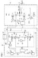
- the actuation circuit according to the invention for a first switch T1 regulating the power consumption of an inductive energy storage element in a switching converter has a signal generating circuit 40, which provides a pulse-width-modulated actuating signal S1, and a measuring and regulating arrangement 20.
- the measuring and regulating arrangement 20 is configured so as to simulate a current measurement signal Vc, which is at least approximately proportional to a current across the inductive storage element, from a single sampled value of an actually measured current signal Vs during an actuation period of the first switch T1 and from other known parameters.
- the current measurement signal Vc generated by the measuring and regulating arrangement 20 is therefore designated hereinbelow as the simulated current measurement signal Vc, while the signal Vs which is sampled in order to generate the single sampled value is designated the actual measurement signal.
- FIG. 1 shows moreover the converter stage of a switching converter, which will be briefly explained hereinbelow.
- the converter stage configured in the example as a buck converter stage, comprises the first switch T1, actuated by the actuating signal S1 of the actuator circuit, and in series with the switch T1 the inductive storage element Lout, for example, a storage induction coil.
- the inductive storage element L forms, together with an output capacitor Cout connected in series with it, a low-pass filter, to furnish an output voltage Vout for a load which can be connected to the converter stage. Connection terminals of the output capacitor Cout form the output terminals of the converter stage.
- a freewheeling element T2 Connected in parallel to the series circuit with the inductive storage element Lout and the output capacitor Cout is a freewheeling element T2.
- the freewheeling element which serves to take over the current across the inductance Lout after the blocking of the first switch T1
- the example uses a second semiconductor switch T2, which is actuated in complementary fashion to the first semiconductor switch T1.
- a first driver circuit 12 is provided, which converts the level of the actuating signal S1 to a level suitable for actuating the first semiconductor switch T1.
- the two semiconductor switches in the example are configured as n-channel MOSFETs. During operation, one must ensure that the two semiconductor switches T1, T2 are not simultaneously conducting.
- the actuating of the second semiconductor switch T2 likewise occurs in accordance with the actuating signal S1, which is inverted by means of an inverter 15 for the actuating of the second semiconductor switch.
- the output signal of the inverter is furnished to a second driver circuit, which converts the level of the signal at the output of the inverter to a level suitable for actuating the second switch T2.
- An input voltage Vin is imposed on the converter stage across the series circuit, which comprises the first switch T1 and the parallel circuit with the filter Lout, Cout, and the freewheeling element.
- the represented converter stage functions as is briefly explained hereinbelow: Under pulse-width-modulated actuation of the first switch T1, a rectangular voltage relative to the reference potential GND is present at the junction node N between the first switch T1 and the inductance, whose amplitude varies between the value of the input voltage Vin and zero. This rectangular voltage is converted by the low-pass filter with the inductance Lout and the capacitor Cout into the approximately uniform output voltage Vout.
- the value of this output voltage Vout for identical input voltage, can be adjusted via the keying ratio of the pulse-width-modulated signal S1. Given identical load and identical input voltage, the output voltage Vout will be larger according as the keying ratio (duty cycle) is larger.
- the duty cycle is defined in terms of the quotient of the on-period of the first switch T1 and the period duration of one actuation period.
- the current Iout flowing through the inductive storage element Lout has a triangular-shaped curve, as is represented by means of Figure 4a for one actuation period.
- the current Iout rises when the first switch T1 is conducting during an on-period of duration Ton and decreases when the first switch is blocked during an off-period of duration Toff.
- a voltage is present across the inductance Lout - disregarding switching losses in the first switch T1 - corresponding to the difference between the input voltage Vin and the output voltage Vout.
- a regulator 14 In order to regulate the output voltage Vout to a given nominal/reference voltage Vref, a regulator 14 is present, which compares the output voltage Vout to the nominal value Vref and produces a regulating signal S14.
- the regulator 14 is configured, for example, as a regulator with integrating behavior (I-regulator), a regulator with proportional-integral behavior (PI-regulator), or a regulator with proportional behavior (P-regulator).
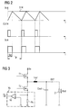
- the pulse width modulator 40 generates the actuating signal S1 (referring to Figure 2) in such a way that the actuating signal S1 assumes an on-level during the pulse of a clock signal CLK, by which the first switch T1 is switched on.
- the first switch T1 is switched on, the current through the inductance Lout, and accordingly the current measurement signal Vc, increase.
- the actuating signal switches from the on-level, or the high level in the example, to an off-level, or a low level in the example, when the current measurement signal Vc reaches the level of the regulating signal S14.
- the on-period Ton and, thus, the duty cycle of the actuating signal S1 varies with the regulating signal S14. If the regulating signal rises, other parameters being equal, then the on-period per actuation period is longer and the power consumption increases. Furthermore, by making use of the measurement signal Vc, proportional to the current Iout through the inductance Lout, the regulating process can take into account changes in the input voltage Vin. If the input voltage Vin increases, shorter on-periods are sufficient to achieve a given power consumption - dictated by the load and the nominal value of the output voltage. Since the inductance current Iout according to (1a) rises with increasing input voltage Vin, the measurement signal reaches the value of the regulating signal S14 more quickly when the input voltage Vin is greater, which automatically produces a shortening of the on-period Ton.
- this current Iout has a triangular-shaped function, in which the slope of rising edges when the first switch T1 is switched on depends according to (1a) on the difference between the input and the output voltage Vin, Vout, and where the slope of falling edges when the first switch T1 is switched off depends according to (1b) on the output voltage Vout.
- the current measuring arrangement 20 forms the current measurement signal Vc from the input voltage Vin, the output voltage Vout, and at least one sampled value of the current across the inductance or one sampled value of an actual current measurement signal.
- the input voltage Vin and the output voltage Vout can be easily measured in a switching converter. It is also easily possible to determine a sampled value of the current Iout across the inductance Lout during an actuation period as compared to determining the current Iout during the entire period.
- the current across the inductance Iout can be easily determined during the on-period or during the off-period, whereas a measurement during the entire period is significantly more difficult.
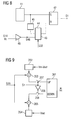
- the current across the inductance Lout is detected during an off-period of the first switch T1, i.e., during the freewheeling time, during which a current is flowing through the freewheeling element T2.
- the current is detected by a current measurement arrangement 11 connected in series to the freewheeling element T2, which produces a current measurement signal Vs proportional to the current across the inductance during the off-period.
- This current measuring arrangement 11 (referring to Figure 3) comprises, for example, a measuring resistor Rs switched in series with the freewheeling element T2 and a measuring amplifier 16 connected to the measuring resistor, which produces, from a voltage drop across the measuring resistor Rs, the measurement signal Vs, which is sent to the measuring and regulating arrangement 20.
- the first exemplary embodiment of the measuring and regulating arrangement depicted in Figure 1 has, for the purpose of simulating the inductance current Iout and producing the simulated current measurement signal Vc, a capacitive storage element C, from which the simulated current measurement signal Vc can be picked off.
- This capacitive storage element is connected to a regulated charging and discharging circuit, which provides a charging current Ic or a discharging current Id for the capacitive storage element C depending on the actuating signal S1.
- This charging and discharging circuit has a first voltage-controlled current source 21, which provides a current I21 proportional to the difference between the input voltage Vin and the output voltage Vout, and the charging and discharging circuit has a second voltage-controlled current source 22, which provides a current I22 proportional to the output voltage Vout.
- Voltage-controlled current sources are sufficiently well known for a detailed discussion as to their layout and functioning to be unnecessary here.
- the first voltage-controlled current source 21 is part of a charging circuit, which is actuated by the pulse-width-modulated actuating signal S1 and charges the capacitive storage element when the first switch T1 is gated in conducting mode.
- the charging circuit is connected between a terminal for power supply potential Vcc and the capacitive storage element C and it has a switch 25 actuated by the actuating signal S1, which enables a current to flow to the capacitive storage element C when the actuating signal S1 adopts a level at which the first switch T1 is gated in conducting mode.
- the charging circuit furthermore, comprises a current amplifier 23, which amplifies the current delivered by the first voltage-controlled current source with a regulating signal value S29 produced by a regulating circuit 29.
- this current amplifier 23 is depicted as a multiplier, which is connected in the current path between the current source 21 and the capacitive storage element.
- a multiplication of the current I21 provided by the voltage-controlled current source 21 with the regulating signal value S29 is of course tantamount to a multiplication of the control signal furnished to the current source 21, being proportional to the difference between input voltage Vin and output voltage Vout, with the regulating signal value S29.
- a multiplier is not connected in the current path between the current source 21 and the capacitive storage element C, but instead is connected ahead of the control input of the current source 21 (not shown).
- a charging current provided by the explained charging circuit is designated in Figure 1 by the reference symbol Ic.
- the second voltage-controlled current source 22 is part of a discharge circuit, which is activated by the pulse-width-modulated actuating signal S1 and discharges the capacitive storage element C when the first switch T1 is gated in blocking mode.
- the discharge circuit is connected between the capacitive storage element C and a terminal for reference potential GND and it has a switch 26, which allows a current to flow to the capacitive storage element C when the actuating signal S1 assumes a level at which the first switch T1 is gated in blocking mode. For this, this switch 26 is activated across an inverter by the actuating signal S1.
- the discharge circuit furthermore, contains a current amplifier 24, which amplifies the current I22 produced by the second voltage-controlled current source 22 with the regulating signal value S29 produced by a regulating circuit 29.
- this current amplifier is shown as a multiplier, which is connected in the current path between the second current source 22 and the capacitive storage element C.
- a multiplication of the current I22 delivered by the voltage-controlled current source 22 with the regulating signal value S29 is of course tantamount to a multiplication of the control signal furnished to the current source 22, which is proportional to the output voltage Vout, with the regulating signal value S29.
- a multiplier is not connected in the current path between the current path 22 and the capacitive storage element C, but instead is connected in series with the control input of the current source 22 (not shown).
- a discharging current produced by the explained discharge circuit is designated as Id in Figure 1.
- V c ( t ) V 0 ⁇ ⁇ V / 2 + m C 1 ⁇ t for 0 ⁇ t ⁇ T on
- V c ( t ) V 0 ⁇ ⁇ V / 2 ⁇ m C 2 ⁇ ( t ⁇ T on ) for T on ⁇ t ⁇ T off
- V0 is the instantaneous mean value of the voltage across the capacitive storage element C and ⁇ V is the amplitude of the triangular function during the actuation period.
- k designates the proportionality factor between the charging current Ic and the difference between the input voltage and output voltage Vin-Vout and the proportionality factor between the discharging current Id and the output voltage Vout.
- the proportionality factor k corresponds in magnitude to the instantaneous value of the regulating signal value S29.
- the proportionality factors between the current I21 of the first current source 21 and the input voltage/output voltage difference Vin-Vout and between the current I22 of the second current source 22 and the output voltage Vout are then equal 1 ampere/volt.
- the time plot of the simulated current measurement signal Vc during an actuation period of the actuating signal is illustrated in Figure 4b.
- the purpose of the measuring and regulating arrangement is to adjust this time function so that it is proportional to the time function of the current across the inductance Iout.
- I out ( t ) I 0 ⁇ ⁇ I / 2 + m L 1 ⁇ t for 0 ⁇ t ⁇ T on
- I out ( t ) I 0 + ⁇ I / 2 ⁇ m L 2 ⁇ ( t ⁇ T on ) for T on ⁇ t ⁇ T on
- m L 1 ( V in ⁇ V out ) / L
- m L 2 V out / L
- I0 here is the instantaneous mean value of the current and ⁇ I is the amplitude of the triangular-shaped function of the current Iout during the actuation period under consideration.
- the value of the externally connected inductance Lout in the current measuring arrangement 20 is not known - unlike the capacitance value of the capacitive storage element C, which can be adjusted exactly when designing the circuit.
- the current measuring arrangement 20 has a loop with the regulating signal circuit 29.
- the purpose of this regulating arrangement is to control the gain of the amplification arrangements 23, 24 of the charging and discharging circuits so that the proportionality factor between the simulated current measurement signal Vc and the inductance current Iout corresponds to the proportionality factor between the actually measured current measurement signal Vs and the inductance current Iout.
- V c ( t ) A i ⁇ R s ⁇ I out ( t )
- Ai the gain of the amplifier 16
- Rs the value of the measuring resistor
- the regulating signal circuit 29, which establishes, via the regulating signal S29, the proportionality factor between the charging current Ic and the input voltage/output voltage difference Vin-Vout and the proportionality factor between the discharging current Id and the output voltage, receives a first sampled signal Vs(k) and a second sampled signal Vc(k).
- the first sampled signal Vs(k) corresponds to a sampled value of the current measurement signal Vs at a given time during a period of the actuating signal S1
- the second sampled signal corresponds to a sampled value of the simulated current measurement signal Vc during the same sampling time of the actuation period.
- a first sampling device 27 which produces the first sampled signal Vs(k), and for the sampling of the simulated current measurement signal Vc there is provided a second sampling device 28, which produces the second sampled signal Vc(k).
- the sampling is done in accordance with the actuating signal S1 each time at a given moment within an actuation period, for example, a given interval after the start of the on-period or after the start of the off-period.
- the regulating signal circuit 29 is configured so as to update the regulating signal S29 at the start of each actuation period of the actuating signal, by multiplying a regulating signal value S29(k) present during a k-th actuation period with the quotient of the first and second sampled value, in order to form a regulating signal value S29 (k+1) for the following k+1-th actuation period.
- S 29 ( k + 1 ) S 29 ( k ) ⁇ ( V s ( k ) / V c ( k ) )
- the regulating signal circuit 29 comprises a divider 291, which receives the first and second sampled value Vs(k), Vc(k), and outputs the quotient Vs(k)/Vc(k) of these two sampled values.
- the regulating signal circuit 29, furthermore, comprises a storage, which outputs the instantaneous regulating signal value S29(k). This instantaneous regulating signal value is fed back to an input of a multiplier 292, the other input of which receives the quotient Vs(k)/Vc(k).
- the signal value Vs(k)/Vc(k) ⁇ S29(k) present at the output of the multiplier is furnished to an input of the storage, in order to update the stored value once per actuation period.
- the updating of this value in the storage 293 occurs, for example, in accordance with the actuating signal S1 at the start of each actuation period.
- a clock signal dictating the cycle of the actuating signal S1 such as a clock signal CLK explained in connection with Figure 2, could of course also be used to update the storage.
- the signal Vs(t) in Figure 6 represents a signal proportional to the inductance current Iout according to relation (7), which corresponds for a segment - during the off-period Toff in the example - to the signal produced by the measurement arrangement 11.
- the slope of the two signals Vc(t), Vs(t) is proportional during the on-period Ton to the input voltage/output voltage difference Vin-Vout, while the slope during the off-period Toff is proportional to the output voltage Vout.
- the simulated regulating signal Vc(t) in the example at first rises more steeply than the actual measurement signal Vs(t) and accordingly drops more steeply, i.e., the proportionality factor between the input/output voltage difference Vin-Vout and the charging current Ic and between the output voltage Vout and the discharging current Id is not adjusted to the desired value.
- sampled values of the simulated signal Vc(t) and the measurement signal Vs(t) are determined at any given time t0 during the actuation period.
- V s ( k ) / V c ( k ) A i ⁇ R s ⁇ C / ( L out ⁇ S 29 ( k ) )
- sampling of the time functions of the two signals Vs(t), Vc(t) can occur at any given time during an actuation period.
- a sampling occurs during the falling edge, because the measurement arrangement 11 according to Figure 11 is configured to generate the measurement signal Vs only during the falling edge, so that only during the falling edge is a comparison value available for the simulated measurement signal Vc.
- the simulated measurement signal Vc in the above-explained example is generated such that its time function follows a measurement signal Vs obtained by multiplying the inductance current Iout with the factor Ai ⁇ Rs.
- a measurement signal is furnished by the measurement arrangement 11 during the off-period in the example of Figure 1.
- This proportionality factor is dependent on the parameters of the measurement arrangement. If a different proportionality factor should be desired, the possibility exists of connecting an amplifier between the regulating arrangement 29 and the charging and discharging circuit.
- the current measurement arrangement has a calibration arrangement, which is configured so as to supply a calibration current Iadj to the capacitive storage element.
- Figure 7 shows the time functions of a signal Vs proportional to the inductance current, the simulated measurement signal Vc before, during, and after the calibration process, and the time function of a calibration current during the calibration process.
- the time functions of the signal Vs proportional to the inductance current, which corresponds for a segment to the signal generated by the measurement arrangement 11, and the simulated signal Vc have different d.c. signal components, which make it difficult or impossible to adapt the time function of the simulated signal Vc to the time function of the signal Vs by merely changing the charging and discharging currents.
- the calibration current Iadj flowing during the calibration is used to adapt the d.c. signal component of the simulated signal Vc to the d.c. signal component of the signal Vs.
- I adj C / T 1 ⁇ ( V s ( i ) ⁇ V c ( i ) )
- the calibration current Iadj is thus dependent on the difference between the sampled values Vs(i), Vc(i) and is generated in the layout according to Figure 1 by a transconductance amplifier (OTA) 31, whose input receives the two sampled values, and which has the desired gain factor, which according to (15) is dependent on the known capacitance value of the capacitive storage element C and the known time position of the sampling time within the actuation period.
- OTA transconductance amplifier
- the calibration phase will comprise at least the period before the actual calibration, during which the sampled values Vs(i), Vc(i) are determined (which corresponds to the period before time t1 in Figure 7), and the actuation period during which the calibration current Iadj flows (corresponding to the period after the time t1 in Figure 7).
- the sampled values Vc(i) and Vc(i) obtained by sampling Vs and Vc signal are stored, for example in the sampling units 27, 28 of figure 1. These sampling values are used for calculating the difference Vs(i)-Vc(i) which is required for calculating the adjustment current Iadj in the OTA.
- the charge and discharge currents are not updated, i.e. there is a fixed proportional factor between the charge current Ic and the input-output voltage difference Vin-Vout and the same fixed proportional factor between the discharge current and the output voltage starting with the time, when the voltage across the capacitor is zero and the current through the inductor is zero.
- the d.c. offset between Vc and Vs is the same during the period when Vs(i) and Vc(i) are obtained and at the beginning of the period when the calibration current is applied.
- the controlling of the calibration process occurs (see Figure 1) via a control circuit 32, which enables the generating of the calibration current Iadj by the amplifier 31 via an enabling signal EN, which is likewise represented in Figure 7.
- This control circuit 32 also controls the pulse width modulator 40 via another control signal S32, so as to bring about the generating of an actuating signal S1 with a constant duty cycle during the calibration phase.
- the pulse width modulator 40 has, for example, a clock generator 41, which produces a clock signal CLK, specifying the start of the on-periods of the actuating signal S1 and, thus, the cycle of the actuating signal S1.
- This clock signal CLK is furnished to the set input of a RS flip-flop, whose output Q produces the actuating signal S1.
- a resetting of the flip-flop 42, and thus the generating of an off-level, occurs during normal operation after the calibration is complete, dependent on a comparing of the simulated measurement signal Vc and the regulating signal S14.
- a comparator 56 for the comparing of these two signals, there is a comparator 56, whose output signal S46 resets the flip-flop 42 during normal operation.
- a multiplexer 44 For switching between calibration mode and normal operation, there is a multiplexer 44, which is actuated by the control signal S32 of the control circuit 32 and which furnishes the comparator signal S46 to the reset input of the flip-flop 42 during normal operation.
- a delay element 45 is provided, which receives the clock signal CLK and whose output signal is furnished to the reset input of the flip-flop 42 during calibration mode. The length of the delay of this delay element determines a constant on-period Ton during calibration mode and, thus, a constant duty cycle.
- this simulated signal can also be produced as a digital signal (see Figure 9).
- the capacitive storage element according to Figure 1 is replaced here by a digital counter 201, which outputs the simulated measurement Vc in the form of a digital numerical value.
- the counter has a first clock input for incrementing the count and a second input for decrementing the count.
- the current sources according to Figure 1 are replaced in this embodiment by a first and second voltage-controlled oscillator (VCO) 202, 204, which have first and second clock signals for incrementing and decrementing the count.
- the clock signals of the voltage-controlled oscillators are furnished to frequency multipliers, which multiply the clock frequency with the preferably likewise digitally produced regulating signal S29.
- the frequency-multiplied clock signal of the first oscillator 202 whose frequency is proportional to the input voltage/output voltage difference Vin-Vout, is furnished to the increment input during the on-period of the actuating signal S1 via a first switch 207, activated by the actuating signal S1.
- the frequency-multiplied clock signal of the second oscillator 204 whose frequency is proportional to the output voltage Vout, is furnished to the decrement input during the off-period of the actuating signal S1 via a second switch 208, activated by the inverted actuating signal S1.
- Both the counter 201 and the previously explained capacitive storage element are part of a triangular signal generating circuit, which simulates the triangular current across the inductance Lout.
Landscapes
- Engineering & Computer Science (AREA)
- Power Engineering (AREA)
- Dc-Dc Converters (AREA)
Priority Applications (3)
| Application Number | Priority Date | Filing Date | Title |
|---|---|---|---|
| EP04020456A EP1632827B1 (fr) | 2004-08-27 | 2004-08-27 | Circuit de commande pour convertisseur abaisseur en mode de courant |
| DE602004006623T DE602004006623T2 (de) | 2004-08-27 | 2004-08-27 | Steuerschaltung für Strombetriebsarten-Abwärtswandler |
| US11/211,381 US7298122B2 (en) | 2004-08-27 | 2005-08-25 | Actuation circuit for a switch regulating the power consumption in a switching converter |
Applications Claiming Priority (1)
| Application Number | Priority Date | Filing Date | Title |
|---|---|---|---|
| EP04020456A EP1632827B1 (fr) | 2004-08-27 | 2004-08-27 | Circuit de commande pour convertisseur abaisseur en mode de courant |
Publications (2)
| Publication Number | Publication Date |
|---|---|
| EP1632827A1 true EP1632827A1 (fr) | 2006-03-08 |
| EP1632827B1 EP1632827B1 (fr) | 2007-05-23 |
Family
ID=34926338
Family Applications (1)
| Application Number | Title | Priority Date | Filing Date |
|---|---|---|---|
| EP04020456A Expired - Lifetime EP1632827B1 (fr) | 2004-08-27 | 2004-08-27 | Circuit de commande pour convertisseur abaisseur en mode de courant |
Country Status (3)
| Country | Link |
|---|---|
| US (1) | US7298122B2 (fr) |
| EP (1) | EP1632827B1 (fr) |
| DE (1) | DE602004006623T2 (fr) |
Cited By (2)
| Publication number | Priority date | Publication date | Assignee | Title |
|---|---|---|---|---|
| US8860393B2 (en) | 2012-12-28 | 2014-10-14 | Dialog Semiconductor Gmbh | Phase lock loop controlled current mode buck converter |
| EP2882085A1 (fr) * | 2013-12-03 | 2015-06-10 | EM Microelectronic-Marin SA | Convertisseur DC-DC à fonctionnement en mode discontinu |
Families Citing this family (25)
| Publication number | Priority date | Publication date | Assignee | Title |
|---|---|---|---|---|
| JP3916163B2 (ja) * | 2004-02-19 | 2007-05-16 | ローム株式会社 | 電流方向検出回路及びそれを備えたスイッチングレギュレータ |
| US8395365B2 (en) * | 2005-11-11 | 2013-03-12 | Maxim Integrated Products, Inc. | Non-linear PWM controller |
| US7816900B2 (en) | 2006-04-05 | 2010-10-19 | International Rectifier Corporation | Correction circuit for improved load transient response |
| JP2007327804A (ja) * | 2006-06-07 | 2007-12-20 | Nec Electronics Corp | 電圧降下測定回路 |
| US20100162024A1 (en) * | 2008-12-24 | 2010-06-24 | Benjamin Kuris | Enabling a Charge Limited Device to Operate for a Desired Period of Time |
| US8674727B2 (en) * | 2010-08-31 | 2014-03-18 | Infineon Technologies Austria Ag | Circuit and method for driving a transistor component based on a load condition |
| US8736363B2 (en) * | 2010-09-13 | 2014-05-27 | Cadence Ams Design India Private Limited | Circuit for optimizing a power management system during varying load conditions |
| US9588532B2 (en) * | 2012-03-26 | 2017-03-07 | Infineon Technologies Americas Corp. | Voltage regulator having an emulated ripple generator |
| US9285399B2 (en) | 2012-06-29 | 2016-03-15 | Infineon Technologies Austria Ag | Switching regulator cycle-by-cycle current estimation |
| US9065337B2 (en) * | 2013-02-25 | 2015-06-23 | Analog Devices Global | Inductor current emulation circuit for a switching converter |
| US9048734B2 (en) * | 2013-03-01 | 2015-06-02 | Analog Devices Global | Negative current protection system for low side switching converter FET |
| US9455631B2 (en) | 2013-09-06 | 2016-09-27 | Infineon Technologies Austria Ag | Current estimation for a converter |
| US9219414B2 (en) * | 2013-10-28 | 2015-12-22 | Analog Devices Global | Load current readback and average estimation |
| US9379615B2 (en) | 2014-09-17 | 2016-06-28 | Stmicroelectronics S.R.L. | High-efficiency energy harvesting interface and corresponding energy harvesting system |
| US10193442B2 (en) | 2016-02-09 | 2019-01-29 | Faraday Semi, LLC | Chip embedded power converters |
| DE102017127263B4 (de) * | 2017-11-20 | 2021-02-18 | Infineon Technologies Ag | Schaltwandler, der pulsweitenmodulation und currentmode-steuerung verwendet |
| US10797579B2 (en) * | 2018-11-02 | 2020-10-06 | Texas Instruments Incorporated | Dual supply low-side gate driver |
| US10504848B1 (en) | 2019-02-19 | 2019-12-10 | Faraday Semi, Inc. | Chip embedded integrated voltage regulator |
| US11069624B2 (en) | 2019-04-17 | 2021-07-20 | Faraday Semi, Inc. | Electrical devices and methods of manufacture |
| US11063516B1 (en) | 2020-07-29 | 2021-07-13 | Faraday Semi, Inc. | Power converters with bootstrap |
| CN112782633A (zh) * | 2020-12-24 | 2021-05-11 | 深圳市优优绿能电气有限公司 | 一种电感电流采样校准方法、系统和计算机可读存储介质 |
| US12339303B2 (en) | 2022-06-08 | 2025-06-24 | Texas Instruments Incorporated | Inductance detection for power converters |
| WO2023239850A1 (fr) * | 2022-06-08 | 2023-12-14 | Texas Instruments Incorporated | Détection d'inductance de convertisseurs de puissance |
| US11990839B2 (en) | 2022-06-21 | 2024-05-21 | Faraday Semi, Inc. | Power converters with large duty cycles |
| CN116578154B (zh) * | 2023-06-13 | 2023-11-21 | 陕西四方华能电气设备有限公司 | 一种调压器的电压自动追踪方法及系统 |
Citations (3)
| Publication number | Priority date | Publication date | Assignee | Title |
|---|---|---|---|---|
| US6166528A (en) * | 1999-11-02 | 2000-12-26 | Fairchild Semiconductor Corporation | Lossless current sensing in buck converters working with low duty cycles and high clock frequencies |
| US6246220B1 (en) * | 1999-09-01 | 2001-06-12 | Intersil Corporation | Synchronous-rectified DC to DC converter with improved current sensing |
| US6381159B2 (en) * | 2000-03-21 | 2002-04-30 | International Rectifier Corp. | Inductor current synthesizer for switching power supplies |
Family Cites Families (8)
| Publication number | Priority date | Publication date | Assignee | Title |
|---|---|---|---|---|
| US5481178A (en) * | 1993-03-23 | 1996-01-02 | Linear Technology Corporation | Control circuit and method for maintaining high efficiency over broad current ranges in a switching regulator circuit |
| JPH09140126A (ja) * | 1995-05-30 | 1997-05-27 | Linear Technol Corp | 適応スイッチ回路、適応出力回路、制御回路およびスイッチング電圧レギュレータを動作させる方法 |
| US5705919A (en) * | 1996-09-30 | 1998-01-06 | Linear Technology Corporation | Low drop-out switching regulator architecture |
| US5912552A (en) * | 1997-02-12 | 1999-06-15 | Kabushiki Kaisha Toyoda Jidoshokki Seisakusho | DC to DC converter with high efficiency for light loads |
| US5847554A (en) * | 1997-06-13 | 1998-12-08 | Linear Technology Corporation | Synchronous switching regulator which employs switch voltage-drop for current sensing |
| US6215290B1 (en) * | 1999-11-15 | 2001-04-10 | Semtech Corporation | Multi-phase and multi-module power supplies with balanced current between phases and modules |
| US6400126B1 (en) * | 1999-12-30 | 2002-06-04 | Volterra Semiconductor Corporation | Switching regulator with multiple power transistor driving voltages |
| US6377034B1 (en) * | 2000-12-11 | 2002-04-23 | Texas Instruments Incorporated | Method and circuits for inductor current measurement in MOS switching regulators |
-
2004
- 2004-08-27 DE DE602004006623T patent/DE602004006623T2/de not_active Expired - Lifetime
- 2004-08-27 EP EP04020456A patent/EP1632827B1/fr not_active Expired - Lifetime
-
2005
- 2005-08-25 US US11/211,381 patent/US7298122B2/en active Active
Patent Citations (3)
| Publication number | Priority date | Publication date | Assignee | Title |
|---|---|---|---|---|
| US6246220B1 (en) * | 1999-09-01 | 2001-06-12 | Intersil Corporation | Synchronous-rectified DC to DC converter with improved current sensing |
| US6166528A (en) * | 1999-11-02 | 2000-12-26 | Fairchild Semiconductor Corporation | Lossless current sensing in buck converters working with low duty cycles and high clock frequencies |
| US6381159B2 (en) * | 2000-03-21 | 2002-04-30 | International Rectifier Corp. | Inductor current synthesizer for switching power supplies |
Non-Patent Citations (1)
| Title |
|---|
| ZAOHONG YANG ET AL: "DC-to-DC buck converters with novel current mode control", POWER ELECTRONICS SPECIALISTS CONFERENCE, 1999. PESC 99. 30TH ANNUAL IEEE CHARLESTON, SC, USA 27 JUNE-1 JULY 1999, PISCATAWAY, NJ, USA,IEEE, US, 27 June 1999 (1999-06-27), pages 1158 - 1164, XP010346831, ISBN: 0-7803-5421-4 * |
Cited By (5)
| Publication number | Priority date | Publication date | Assignee | Title |
|---|---|---|---|---|
| US8860393B2 (en) | 2012-12-28 | 2014-10-14 | Dialog Semiconductor Gmbh | Phase lock loop controlled current mode buck converter |
| EP2882085A1 (fr) * | 2013-12-03 | 2015-06-10 | EM Microelectronic-Marin SA | Convertisseur DC-DC à fonctionnement en mode discontinu |
| EP2882087A1 (fr) * | 2013-12-03 | 2015-06-10 | EM Microelectronic-Marin SA | Convertisseur DC-DC à fonctionnement en mode discontinu |
| US9391520B2 (en) | 2013-12-03 | 2016-07-12 | Em Microelectronic-Marin Sa | Discontinuous mode DC-DC converter including a voltage-current conversion circuit for converting into current a difference between an output voltage and an input voltage of switches of the converter |
| TWI657652B (zh) * | 2013-12-03 | 2019-04-21 | 瑞士商艾姆微體電子 馬林公司 | 不連續模式直流對直流轉換器及其致動方法 |
Also Published As
| Publication number | Publication date |
|---|---|
| DE602004006623D1 (de) | 2007-07-05 |
| EP1632827B1 (fr) | 2007-05-23 |
| US7298122B2 (en) | 2007-11-20 |
| DE602004006623T2 (de) | 2008-01-17 |
| US20060061342A1 (en) | 2006-03-23 |
Similar Documents
| Publication | Publication Date | Title |
|---|---|---|
| EP1632827B1 (fr) | Circuit de commande pour convertisseur abaisseur en mode de courant | |
| US6225795B1 (en) | Discrete-time sampling of data for use in switching regulations | |
| US8194420B2 (en) | Method for controlling a switching regulator and related switching regulator | |
| US10181792B2 (en) | Sensor-less buck current regulator with average current mode control | |
| US7605573B2 (en) | Switching regulator providing slope compensation and voltage control method thereof | |
| US7126318B2 (en) | Higher order slope compensation for fixed frequency current mode switching regulators | |
| CN101828327B (zh) | Dc/dc变换装置和dc/dc变换方法 | |
| US6377032B1 (en) | Method and apparatus for virtual current sensing in DC-DC switched mode power supplies | |
| US6922044B2 (en) | Synchronization of multiphase synthetic ripple voltage regulator | |
| US8049474B2 (en) | Switching converter with plural converter stages having calibrated current uptake | |
| US6307361B1 (en) | Method and apparatus for regulating the input impedance of PWM converters | |
| US7239117B2 (en) | Programmable inductor current control for DC-DC converters | |
| US20090146634A1 (en) | Single integrator sensorless current mode control for a switching power converter | |
| US20070085523A1 (en) | Dc-dc converter | |
| EP2885861B1 (fr) | Contrôleur à mode de courant pour convertisseur abaisseur de tension (buck) | |
| CN110957894B (zh) | 电感型开关电源转换器的负载电流检测方法及电路 | |
| CN101398670B (zh) | 对具有积分响应的系统的基于时间的控制器和控制方法 | |
| KR100576373B1 (ko) | 디지털 모듈레이션 기법을 이용한 디지털 dc-dc 컨버터 | |
| US6992468B2 (en) | Boost regulator utilizing a digital controller | |
| US10044269B2 (en) | Switching converter with improved recovery time | |
| US20210099082A1 (en) | Peak current limit in a slope-compensated current mode dc-dc converter | |
| US6930526B1 (en) | Quasi-feedforward PWM modulator | |
| US6285174B1 (en) | Switching DC-to-Dc converter having on-time signal generation circuit and method for generating signal indicative of converter on-time | |
| US12301091B2 (en) | Artificial dual closed-loop full-time inductor current sensing | |
| EP4537447A1 (fr) | Détection d'inductance de convertisseurs de puissance |
Legal Events
| Date | Code | Title | Description |
|---|---|---|---|
| PUAI | Public reference made under article 153(3) epc to a published international application that has entered the european phase |
Free format text: ORIGINAL CODE: 0009012 |
|
| 17P | Request for examination filed |
Effective date: 20050309 |
|
| AK | Designated contracting states |
Kind code of ref document: A1 Designated state(s): AT BE BG CH CY CZ DE DK EE ES FI FR GB GR HU IE IT LI LU MC NL PL PT RO SE SI SK TR |
|
| AX | Request for extension of the european patent |
Extension state: AL HR LT LV MK |
|
| AKX | Designation fees paid |
Designated state(s): DE GB |
|
| GRAP | Despatch of communication of intention to grant a patent |
Free format text: ORIGINAL CODE: EPIDOSNIGR1 |
|
| GRAS | Grant fee paid |
Free format text: ORIGINAL CODE: EPIDOSNIGR3 |
|
| GRAA | (expected) grant |
Free format text: ORIGINAL CODE: 0009210 |
|
| AK | Designated contracting states |
Kind code of ref document: B1 Designated state(s): DE GB |
|
| REG | Reference to a national code |
Ref country code: GB Ref legal event code: FG4D |
|
| REF | Corresponds to: |
Ref document number: 602004006623 Country of ref document: DE Date of ref document: 20070705 Kind code of ref document: P |
|
| PLBE | No opposition filed within time limit |
Free format text: ORIGINAL CODE: 0009261 |
|
| STAA | Information on the status of an ep patent application or granted ep patent |
Free format text: STATUS: NO OPPOSITION FILED WITHIN TIME LIMIT |
|
| 26N | No opposition filed |
Effective date: 20080226 |
|
| PGFP | Annual fee paid to national office [announced via postgrant information from national office to epo] |
Ref country code: GB Payment date: 20190821 Year of fee payment: 16 |
|
| PGFP | Annual fee paid to national office [announced via postgrant information from national office to epo] |
Ref country code: DE Payment date: 20191015 Year of fee payment: 16 |
|
| REG | Reference to a national code |
Ref country code: DE Ref legal event code: R119 Ref document number: 602004006623 Country of ref document: DE |
|
| GBPC | Gb: european patent ceased through non-payment of renewal fee |
Effective date: 20200827 |
|
| PG25 | Lapsed in a contracting state [announced via postgrant information from national office to epo] |
Ref country code: DE Free format text: LAPSE BECAUSE OF NON-PAYMENT OF DUE FEES Effective date: 20210302 |
|
| PG25 | Lapsed in a contracting state [announced via postgrant information from national office to epo] |
Ref country code: GB Free format text: LAPSE BECAUSE OF NON-PAYMENT OF DUE FEES Effective date: 20200827 |