EP1635183A1 - Vorrichtung zur Überwachung des Ruhestroms einer elektronischen Vorrichtung - Google Patents
Vorrichtung zur Überwachung des Ruhestroms einer elektronischen Vorrichtung Download PDFInfo
- Publication number
- EP1635183A1 EP1635183A1 EP05077673A EP05077673A EP1635183A1 EP 1635183 A1 EP1635183 A1 EP 1635183A1 EP 05077673 A EP05077673 A EP 05077673A EP 05077673 A EP05077673 A EP 05077673A EP 1635183 A1 EP1635183 A1 EP 1635183A1
- Authority
- EP
- European Patent Office
- Prior art keywords
- current
- ddq
- value
- measured
- measurement
- Prior art date
- Legal status (The legal status is an assumption and is not a legal conclusion. Google has not performed a legal analysis and makes no representation as to the accuracy of the status listed.)
- Granted
Links
- 238000012544 monitoring process Methods 0.000 title description 2
- 238000005259 measurement Methods 0.000 claims abstract description 48
- 238000012360 testing method Methods 0.000 claims abstract description 27
- 238000012545 processing Methods 0.000 claims description 16
- 239000013598 vector Substances 0.000 description 17
- 230000007547 defect Effects 0.000 description 8
- 238000000034 method Methods 0.000 description 6
- 230000001052 transient effect Effects 0.000 description 3
- 230000035945 sensitivity Effects 0.000 description 2
- 238000013459 approach Methods 0.000 description 1
- 230000003247 decreasing effect Effects 0.000 description 1
- 230000001419 dependent effect Effects 0.000 description 1
- 238000001514 detection method Methods 0.000 description 1
- 238000005516 engineering process Methods 0.000 description 1
- 238000000691 measurement method Methods 0.000 description 1
- 238000012806 monitoring device Methods 0.000 description 1
- 238000012546 transfer Methods 0.000 description 1
Images


Classifications
-
- G—PHYSICS
- G01—MEASURING; TESTING
- G01R—MEASURING ELECTRIC VARIABLES; MEASURING MAGNETIC VARIABLES
- G01R31/00—Arrangements for testing electric properties; Arrangements for locating electric faults; Arrangements for electrical testing characterised by what is being tested not provided for elsewhere
- G01R31/28—Testing of electronic circuits, e.g. by signal tracer
- G01R31/30—Marginal testing, e.g. by varying supply voltage
- G01R31/3004—Current or voltage test
- G01R31/3008—Quiescent current [IDDQ] test or leakage current test
-
- G—PHYSICS
- G01—MEASURING; TESTING
- G01R—MEASURING ELECTRIC VARIABLES; MEASURING MAGNETIC VARIABLES
- G01R31/00—Arrangements for testing electric properties; Arrangements for locating electric faults; Arrangements for electrical testing characterised by what is being tested not provided for elsewhere
- G01R31/28—Testing of electronic circuits, e.g. by signal tracer
- G01R31/317—Testing of digital circuits
- G01R31/3173—Marginal testing
Definitions
- the present invention is related to a device for measuring the quiescent current (I DDQ ) drawn by an electronic device, such as a CMOS device or an Integrated Circuit, when the device is powered by a supply voltage (V DD ).
- I DDQ The current drawn by a powered CMOS device or IC, when it is not in switching mode, is called the 'quiescent current', described by the symbol I DDQ . It is known that the value of this current is a very sensitive criterion for identifying possible malfunctioning of the IC.
- I Total Leakage ( ⁇ ) I Background Leakage ( ⁇ ) + I Defect Leakage ( ⁇ )
- the measurement resolution must be very high throughout the measurement range of the monitor. People skilled in the art know that increasing the measurement range is always done at the expense of measurement resolution. Yet the resolution should remain constant as the defect leakage current remains constant.
- Existing I DDQ monitors do not offer a solution to this problem.
- the present invention aims to provide a device for I DDQ monitoring of electronic devices, which has a high resolution for higher I DDQ levels.
- the device of the application is capable of being used both in on-chip and off-chip applications.
- the invention is related to a device for measuring the supply current (I DDQ ) to an electronic device under test, which is powered by a supply voltage (V DUT ), said measuring device being placed in a supply line between said supply voltage and said device under test, said measuring device comprising a current measuring unit or CMU, a current bypass unit or CBU in parallel to said CMU, characterized in that said measuring device further comprises an offset current device, said offset current device comprising a current source, for providing a constant offset current to said DUT.
- Said current source is preferably programmable. It may be coupled in parallel to said current measuring unit, or it may be powered by a supply voltage (V DD ) which is different from the DUT supply voltage (V DUT ).
- Any device according to the invention may further comprise a processing unit, which is in connection with said current measuring unit and with an output device and which is able to acquire an I DDQ measured value from the CMU, characterized in that the processing unit is able to perform processing actions on said measurement.
- Said processing actions are preferably chosen from the group consisting of :
- a device of the invention may be separate from said device under test, or it may be incorporated into said device under test.
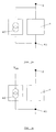
- Fig. 1 represents a schematic view of an I DDQ monitor according to the invention.
- Fig. 2a and 2b represent schematic views of two embodiments of the current offset unit according to the invention.
- Fig. 3 represents a graph, illustrating the application of a virtual measurement window to the leakage current, by using a monitor according to the invention.
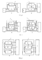
- Figures 4 to 7 illustrate different off-chip and on-chip embodiments of a device according to the invention.
- FIG. 1 illustrates a schematic view of an I DDQ monitoring device or simply named 'monitor' 1, according to the invention.
- the monitor is represented as a separate device, which can for example be incorporated into the test equipment, as a load-board application. It is emphasized that the same monitor can be designed as an on-chip device.
- the monitor 1 is connected by two terminals 2 and 3, between a supply voltage source 4, and the Device-Under-Test DUT 5.
- the supply voltage V DUT at the terminal 2 should be present also, with a minimum error, on the terminal 3, in order to create a maximum transparency of the monitor 1.
- the measurement of the I DDQ is performed by the current measuring unit CMU 6, during a non-switching state of the DUT.
- Test vectors 7 are applied to the DUT at a given clock frequency, by the test equipment 8.
- the CMU 6 may be a unit working according to the stabilized voltage source principle or any other prior art measurement method.
- a current bypass unit CBU 20 is placed parallel to the CMU 6.
- the CBU 20 preferably comprises a power MOSFET which can be closed prior to the occurrence of the transient peak resulting from the DUT's switching action. This transient peak occurs when a test vector is applied to the DUT or when the application of a clock cycle of the DUT's operational clock causes the DUT to change state. In between transient peaks and for the desired measurement states, the MOSFET is normally opened in order to send the quiescent current I DDQ through the current measuring unit CMU 6.
- the operation of the CBU 20 and the Offset Current Unit (OCU) 21, said OCU being characteristic to the invention and described further, is controlled by the processing unit 9, via control signals 10 and 11.
- the PU 9 controls the opening and closing of the MOSFET incorporated in the CBU 20, on the basis of a clock signal derived from the clock with which the DUT is operated.
- the clock applied to the CBU is dependent on the relevant measurement sequence : there is not necessarily a measurement during every clock cycle of the DUT.
- the current measuring unit When in measurement mode, the current measuring unit performs an I DDQ measurement, during a non-switching period of the DUT and delivers a signal 12 related to the I DDQ level, to the processing unit 9, which digitises the signal, and transmits it via the terminal 13, to the test equipment 8.
- the test equipment 8 controls the processing unit 9, and processes the monitor's output 12, so that the result of the I DDQ measurement is displayed on a screen.
- the source 4 is not separate, and the supply voltage V DUT is equally supplied by the test equipment 8.
- the displayed result is at least a pass/fail statement based on the comparison between the measured I DDQ value and a predefined reference, often completed by the measured value of I DDQ .
- Other measurement modes can be selected when using the preferred version of the processing unit 9. For example : the measurement of current signatures or a delta I DDQ measurement mode wherein subsequent measurements are subtracted and the delta-values obtained are memorized and compared to a reference.
- the PU 9 itself performs the processing of the incoming signals, for example the subtraction of two subsequent I DDQ measurement values, before a result is transferred to the test equipment 8.
- Block 21 shown in figure 1 is the characteristic element of the invention. This is the Offset Current Unit (OCU).
- OCU Offset Current Unit
- the background leakage current can be of the order of 100mA, while the defect-related leakage current I DDQdefect is typically between 0 and 10mA.
- the background leakage component can therefore be regarded as an offset current (IDDQ Offset ).
- the OCU 21 is actually a current source 40, delivering an essentially fixed offset current into the supply line to the DUT.
- the current source will deliver a given offset current level I DDQoffset to the summing node 41, so that only the I DDQ above this level is drawn from the current measuring unit 6. In that way a flexible virtual measurement window (VMW) 42 is created with a high measurement resolution (figure 3).
- the offset current source is preferably a programmable current source.
- the offset level 43 which is delivered as an offset current is programmable and variable during the measurement. It is basically controlled by the operator of the test equipment, through the processing unit 8. Two embodiments are considered, as shown in figures 2a and 2b. In figure 2a, the current source 40 is connected to the supply voltage V DUT , placing the OCU in parallel to the CMU. However, a parallel connection is not necessary.
- the offset current unit may for example be connected to the device supply voltage V DD (figure 2b). Autoranging sequences are preferably performed prior to applying a series of test vectors, in order to establish the optimal level of the applied offset current.
- a programmable current source 40 is preferably used.
- the programmable current source 21 can be implemented either as a stand-alone module (figure 4) or it can be part of the off-chip current monitor 100 (figure 5).
- the block 100 in figures 4 to 7 represents an I DDQ monitor with a CMU 6, and preferably with a CBU 20 according to EP application No. 02447125.2.
- the off-chip current monitor architecture is of no importance to the windowing concept.
- the offset current unit 21 can be an add-on core to the Built-In Current Sensor (BICS) (figure 6) or be part of the BICS itself (figure 7).
- BICS Built-In Current Sensor
- the BICS architecture is of no importance to the concept. In all embodiments shown in figures 4-7, the dotted line delineates what is to be understood as the device 1 of the invention.
- the (programmable) current source can be controlled by the ATE 8 (figures 4a, 5a, 6a, 7a) or by the on-chip/off-chip I DDQ monitor (figures 4b, 5b, 6b, 7b) and although it is not necessary, the offset current unit can be part of a auto-windowing procedure. Examples of measurement modes performed by the Processing Unit.
- the following measurement modes comprise calculations which are performed by the processing unit itself. Results of calculations (subtraction of I DDQ values, comparison results) are transferred to the ATE 8 which may further process them or display the results on a screen.
Landscapes
- Engineering & Computer Science (AREA)
- General Engineering & Computer Science (AREA)
- Physics & Mathematics (AREA)
- General Physics & Mathematics (AREA)
- Testing Of Individual Semiconductor Devices (AREA)
- Tests Of Electronic Circuits (AREA)
- Arrangements For Transmission Of Measured Signals (AREA)
Priority Applications (1)
| Application Number | Priority Date | Filing Date | Title |
|---|---|---|---|
| DE60223730T DE60223730T2 (de) | 2002-07-03 | 2002-07-03 | Vorrichtung zur Überwachung des Ruhestroms einer elektronischen Vorrichtung |
Applications Claiming Priority (1)
| Application Number | Priority Date | Filing Date | Title |
|---|---|---|---|
| EP02447125A EP1378758B1 (de) | 2002-07-03 | 2002-07-03 | Vorrichtung zum Messen des Ruhestromes einer elektronischen Vorrichtung |
Related Parent Applications (1)
| Application Number | Title | Priority Date | Filing Date |
|---|---|---|---|
| EP02447125A Division EP1378758B1 (de) | 2002-07-03 | 2002-07-03 | Vorrichtung zum Messen des Ruhestromes einer elektronischen Vorrichtung |
Publications (2)
| Publication Number | Publication Date |
|---|---|
| EP1635183A1 true EP1635183A1 (de) | 2006-03-15 |
| EP1635183B1 EP1635183B1 (de) | 2007-11-21 |
Family
ID=29719827
Family Applications (2)
| Application Number | Title | Priority Date | Filing Date |
|---|---|---|---|
| EP02447125A Expired - Lifetime EP1378758B1 (de) | 2002-07-03 | 2002-07-03 | Vorrichtung zum Messen des Ruhestromes einer elektronischen Vorrichtung |
| EP05077673A Expired - Lifetime EP1635183B1 (de) | 2002-07-03 | 2002-07-03 | Vorrichtung zur Überwachung des Ruhestroms einer elektronischen Vorrichtung |
Family Applications Before (1)
| Application Number | Title | Priority Date | Filing Date |
|---|---|---|---|
| EP02447125A Expired - Lifetime EP1378758B1 (de) | 2002-07-03 | 2002-07-03 | Vorrichtung zum Messen des Ruhestromes einer elektronischen Vorrichtung |
Country Status (4)
| Country | Link |
|---|---|
| US (2) | US6927592B2 (de) |
| EP (2) | EP1378758B1 (de) |
| AT (1) | ATE314658T1 (de) |
| DE (2) | DE60208357T2 (de) |
Families Citing this family (9)
| Publication number | Priority date | Publication date | Assignee | Title |
|---|---|---|---|---|
| CN100395817C (zh) * | 2001-11-14 | 2008-06-18 | 松下电器产业株式会社 | 编码设备、解码设备和解码方法 |
| US6941235B2 (en) * | 2003-10-28 | 2005-09-06 | International Business Machines Corporation | Method and system for analyzing quiescent power plane current (IDDQ) test data in very-large scale integrated (VLSI) circuits |
| GB2431739A (en) * | 2005-10-27 | 2007-05-02 | Wolfson Microelectronics Plc | Switch current sensing circuit |
| US8330483B2 (en) * | 2006-11-29 | 2012-12-11 | Nec Corporation | Semiconductor device to detect abnormal leakage current caused by a defect |
| US7812628B2 (en) * | 2006-12-13 | 2010-10-12 | Renesas Electronics Corporation | Method of on-chip current measurement and semiconductor IC |
| US9651596B2 (en) * | 2013-08-30 | 2017-05-16 | Keysight Technologies, Inc. | System and apparatus for measuring capacitance |
| EP3673276B1 (de) * | 2017-09-25 | 2023-06-07 | Siemens Mobility Pty Ltd. | Einbettung und detektion von codes in überwachungs-signaturen |
| US11668733B2 (en) * | 2018-11-09 | 2023-06-06 | Keithley Instruments, Llc | Multi-stage current measurement architecture |
| CN115357086B (zh) * | 2022-08-29 | 2024-03-08 | 上海壁仞智能科技有限公司 | 带隙基准电路及其操作方法、电子装置 |
Citations (4)
| Publication number | Priority date | Publication date | Assignee | Title |
|---|---|---|---|---|
| EP0386804A2 (de) * | 1989-01-10 | 1990-09-12 | Koninklijke Philips Electronics N.V. | Anordnung zum Ermitteln eines Ruhestroms einer integrierten monolithischen digitalen Schaltung, integrierte monolithische digitale Schaltung mit einer derartigen Anordnung und Prüfgerät mit einer derartigen Anordnung |
| US5483170A (en) * | 1993-08-24 | 1996-01-09 | New Mexico State University Technology Transfer Corp. | Integrated circuit fault testing implementing voltage supply rail pulsing and corresponding instantaneous current response analysis |
| US5914615A (en) * | 1997-04-29 | 1999-06-22 | Hewlett-Packard Company | Method of improving the quality and efficiency of Iddq testing |
| US6414511B1 (en) * | 1999-02-10 | 2002-07-02 | Koninklijke Philips Electronics N.V. | Arrangement for transient-current testing of a digital electronic CMOS circuit |
Family Cites Families (14)
| Publication number | Priority date | Publication date | Assignee | Title |
|---|---|---|---|---|
| US3754442A (en) * | 1970-12-01 | 1973-08-28 | Instrulab Inc | Temperature measuring system producing linear output signal from non-linear sensing resistance |
| US5392293A (en) * | 1993-02-26 | 1995-02-21 | At&T Corp. | Built-in current sensor for IDDQ testing |
| EP0672911A1 (de) | 1994-02-25 | 1995-09-20 | ALCATEL BELL Naamloze Vennootschap | Prüfeinrichtung für Ruheversorgungsstrom |
| US5731700A (en) * | 1994-03-14 | 1998-03-24 | Lsi Logic Corporation | Quiescent power supply current test method and apparatus for integrated circuits |
| US5721495A (en) * | 1995-10-24 | 1998-02-24 | Unisys Corporation | Circuit for measuring quiescent current |
| KR100198617B1 (ko) * | 1995-12-27 | 1999-06-15 | 구본준 | 모오스 캐패시터의 누설전압감지회로 |
| DE69733789T2 (de) * | 1996-06-05 | 2006-06-01 | Interuniversitair Micro-Electronica Centrum Vzw | Hochauflösendes Stromversorgungsprüfsystem |
| US6239604B1 (en) | 1996-10-04 | 2001-05-29 | U.S. Philips Corporation | Method for inspecting an integrated circuit by measuring a voltage drop in a supply line of sub-circuit thereof |
| US6859058B2 (en) * | 1999-05-11 | 2005-02-22 | Interuniversitair Microelektronica Centrum (Imec Uzw) | Method and apparatus for testing electronic devices |
| US6496028B1 (en) * | 1999-05-11 | 2002-12-17 | Interuniversitair Micro-Elektronica Centrum | Method and apparatus for testing electronic devices |
| EP1107013B1 (de) | 1999-09-22 | 2006-06-07 | Interuniversitair Micro-Elektronica Centrum | Verfahren und Vorrichtung zum Testen von Anschlüssen |
| US6342790B1 (en) * | 2000-04-13 | 2002-01-29 | Pmc-Sierra, Inc. | High-speed, adaptive IDDQ measurement |
| US6424211B1 (en) * | 2000-06-26 | 2002-07-23 | Microchip Technology Incorporated | Digital trimming of OP AMP offset voltage and quiescent current using non-volatile memory |
| US6664801B1 (en) * | 2001-05-21 | 2003-12-16 | Lsi Logic Corporation | IDDQ test methodology based on the sensitivity of fault current to power supply variations |
-
2002
- 2002-07-03 DE DE60208357T patent/DE60208357T2/de not_active Expired - Lifetime
- 2002-07-03 EP EP02447125A patent/EP1378758B1/de not_active Expired - Lifetime
- 2002-07-03 AT AT02447125T patent/ATE314658T1/de not_active IP Right Cessation
- 2002-07-03 EP EP05077673A patent/EP1635183B1/de not_active Expired - Lifetime
- 2002-07-03 DE DE60223730T patent/DE60223730T2/de not_active Expired - Lifetime
-
2003
- 2003-07-03 US US10/613,260 patent/US6927592B2/en not_active Expired - Fee Related
-
2005
- 2005-03-15 US US11/085,027 patent/US7315180B2/en not_active Expired - Fee Related
Patent Citations (4)
| Publication number | Priority date | Publication date | Assignee | Title |
|---|---|---|---|---|
| EP0386804A2 (de) * | 1989-01-10 | 1990-09-12 | Koninklijke Philips Electronics N.V. | Anordnung zum Ermitteln eines Ruhestroms einer integrierten monolithischen digitalen Schaltung, integrierte monolithische digitale Schaltung mit einer derartigen Anordnung und Prüfgerät mit einer derartigen Anordnung |
| US5483170A (en) * | 1993-08-24 | 1996-01-09 | New Mexico State University Technology Transfer Corp. | Integrated circuit fault testing implementing voltage supply rail pulsing and corresponding instantaneous current response analysis |
| US5914615A (en) * | 1997-04-29 | 1999-06-22 | Hewlett-Packard Company | Method of improving the quality and efficiency of Iddq testing |
| US6414511B1 (en) * | 1999-02-10 | 2002-07-02 | Koninklijke Philips Electronics N.V. | Arrangement for transient-current testing of a digital electronic CMOS circuit |
Non-Patent Citations (2)
| Title |
|---|
| STRAKA B ET AL: "A fully digital controlled off-chip IDDQ measurement unit", DESIGN, AUTOMATION AND TEST IN EUROPE, 1998., PROCEEDINGS PARIS, FRANCE 23-26 FEB. 1998, LOS ALAMITOS, CA, USA,IEEE COMPUT. SOC, US, 23 February 1998 (1998-02-23), pages 495 - 500, XP010268555, ISBN: 0-8186-8359-7 * |
| SU S-T ET AL: "TRANSIENT POWER SUPPLY CURRENT MONITORING - A NEW TEST METHOD FOR CMOS VLSI CIRCUITS", JOURNAL OF ELECTRONIC TESTING, KLUWER ACADEMIC PUBLISHERS, DORDRECHT, NL, vol. 6, no. 1, 1 February 1995 (1995-02-01), pages 23 - 43, XP000504510, ISSN: 0923-8174 * |
Also Published As
| Publication number | Publication date |
|---|---|
| EP1635183B1 (de) | 2007-11-21 |
| DE60223730D1 (de) | 2008-01-03 |
| DE60208357T2 (de) | 2006-09-14 |
| DE60223730T2 (de) | 2008-10-30 |
| EP1378758B1 (de) | 2005-12-28 |
| ATE314658T1 (de) | 2006-01-15 |
| US20040046576A1 (en) | 2004-03-11 |
| US20050156619A1 (en) | 2005-07-21 |
| DE60208357D1 (de) | 2006-02-02 |
| US7315180B2 (en) | 2008-01-01 |
| EP1378758A1 (de) | 2004-01-07 |
| US6927592B2 (en) | 2005-08-09 |
Similar Documents
| Publication | Publication Date | Title |
|---|---|---|
| KR100249252B1 (ko) | Cmos 집적회로의 고장 검출 시스템 | |
| EP0811850B1 (de) | Hochauflösendes Stromversorgungsprüfsystem | |
| US6246248B1 (en) | Tester for detecting an abnormal quiescent power supply current in a device under test | |
| US6215324B1 (en) | Dynamic burn-in test equipment | |
| US4947106A (en) | Programmatically generated in-circuit test of analog to digital converters | |
| US5789933A (en) | Method and apparatus for determining IDDQ | |
| KR100561557B1 (ko) | 누설 전류 보상회로를 구비하는 테스터 모듈, 집적회로 테스터 및 그 조작 방법 | |
| EP1635183B1 (de) | Vorrichtung zur Überwachung des Ruhestroms einer elektronischen Vorrichtung | |
| EP3290934B1 (de) | Scan-schaltkreis mit iddq prüfung | |
| Stopjakova et al. | CCII+ current conveyor based BIC monitor for I/sub DDQ/testing of complex CMOS circuits | |
| TWI384241B (zh) | 測量設備、測試系統以及測量方法 | |
| Manhaeve et al. | An off-chip IDDq current measurement unit for telecommunication ASICs | |
| JP4314096B2 (ja) | 半導体集積回路検査装置および半導体集積回路検査方法 | |
| KR100431318B1 (ko) | 반도체소자의esd테스트장치및그구동방법 | |
| KR100231649B1 (ko) | 커패시터 충전회로를 갖는 검사용 기판 및 이를이용한 집적회로 검사 방법 | |
| JP4043743B2 (ja) | 半導体試験装置 | |
| US6737671B2 (en) | Current measurement circuit and method for voltage regulated semiconductor integrated circuit devices | |
| JP2963234B2 (ja) | 高速デバイス試験方法 | |
| US20250355037A1 (en) | Device and methods for monitoring parametric data | |
| US6411115B2 (en) | Apparatus for testing a semiconductor and process for the same | |
| WO2025239922A1 (en) | Device and methods for monitoring parametric data | |
| JPH08226942A (ja) | 試験用プローブピンの接触不良判断方法およびインサーキットテスタ | |
| JP2002131368A (ja) | Cmos−lsi試験方法及び装置 | |
| RU2307367C1 (ru) | Вспомогательный блок для индикации контакта измерительного прибора с проверяемым объектом | |
| JP2001296328A (ja) | 被測定装置に対する所定試験項目の試験装置 |
Legal Events
| Date | Code | Title | Description |
|---|---|---|---|
| PUAI | Public reference made under article 153(3) epc to a published international application that has entered the european phase |
Free format text: ORIGINAL CODE: 0009012 |
|
| AC | Divisional application: reference to earlier application |
Ref document number: 1378758 Country of ref document: EP Kind code of ref document: P |
|
| AK | Designated contracting states |
Kind code of ref document: A1 Designated state(s): AT BE BG CH CY CZ DE DK EE ES FI FR GB GR IE IT LI LU MC NL PT SE SK TR |
|
| 17P | Request for examination filed |
Effective date: 20060908 |
|
| 17Q | First examination report despatched |
Effective date: 20061012 |
|
| AKX | Designation fees paid |
Designated state(s): BE DE FR IT |
|
| GRAP | Despatch of communication of intention to grant a patent |
Free format text: ORIGINAL CODE: EPIDOSNIGR1 |
|
| GRAS | Grant fee paid |
Free format text: ORIGINAL CODE: EPIDOSNIGR3 |
|
| GRAA | (expected) grant |
Free format text: ORIGINAL CODE: 0009210 |
|
| AC | Divisional application: reference to earlier application |
Ref document number: 1378758 Country of ref document: EP Kind code of ref document: P |
|
| AK | Designated contracting states |
Kind code of ref document: B1 Designated state(s): BE DE FR IT |
|
| REF | Corresponds to: |
Ref document number: 60223730 Country of ref document: DE Date of ref document: 20080103 Kind code of ref document: P |
|
| PLBE | No opposition filed within time limit |
Free format text: ORIGINAL CODE: 0009261 |
|
| STAA | Information on the status of an ep patent application or granted ep patent |
Free format text: STATUS: NO OPPOSITION FILED WITHIN TIME LIMIT |
|
| 26N | No opposition filed |
Effective date: 20080822 |
|
| PG25 | Lapsed in a contracting state [announced via postgrant information from national office to epo] |
Ref country code: FR Free format text: LAPSE BECAUSE OF FAILURE TO SUBMIT A TRANSLATION OF THE DESCRIPTION OR TO PAY THE FEE WITHIN THE PRESCRIBED TIME-LIMIT Effective date: 20080905 |
|
| PG25 | Lapsed in a contracting state [announced via postgrant information from national office to epo] |
Ref country code: IT Free format text: LAPSE BECAUSE OF NON-PAYMENT OF DUE FEES Effective date: 20080731 |
|
| PGFP | Annual fee paid to national office [announced via postgrant information from national office to epo] |
Ref country code: BE Payment date: 20140623 Year of fee payment: 13 Ref country code: DE Payment date: 20140620 Year of fee payment: 13 |
|
| REG | Reference to a national code |
Ref country code: DE Ref legal event code: R119 Ref document number: 60223730 Country of ref document: DE |
|
| PG25 | Lapsed in a contracting state [announced via postgrant information from national office to epo] |
Ref country code: DE Free format text: LAPSE BECAUSE OF NON-PAYMENT OF DUE FEES Effective date: 20160202 |
|
| PG25 | Lapsed in a contracting state [announced via postgrant information from national office to epo] |
Ref country code: BE Free format text: LAPSE BECAUSE OF NON-PAYMENT OF DUE FEES Effective date: 20150731 |