EP1640326A2 - Methode und System, um ein Gehäuse für ein MEMS-Bauteil mit einer zusätzlichen Dichtung zu versehen - Google Patents
Methode und System, um ein Gehäuse für ein MEMS-Bauteil mit einer zusätzlichen Dichtung zu versehen Download PDFInfo
- Publication number
- EP1640326A2 EP1640326A2 EP05255660A EP05255660A EP1640326A2 EP 1640326 A2 EP1640326 A2 EP 1640326A2 EP 05255660 A EP05255660 A EP 05255660A EP 05255660 A EP05255660 A EP 05255660A EP 1640326 A2 EP1640326 A2 EP 1640326A2
- Authority
- EP
- European Patent Office
- Prior art keywords
- mems device
- seal
- substrate
- backplane
- primary
- Prior art date
- Legal status (The legal status is an assumption and is not a legal conclusion. Google has not performed a legal analysis and makes no representation as to the accuracy of the status listed.)
- Withdrawn
Links
Images


Classifications
-
- H—ELECTRICITY
- H01—ELECTRIC ELEMENTS
- H01R—ELECTRICALLY-CONDUCTIVE CONNECTIONS; STRUCTURAL ASSOCIATIONS OF A PLURALITY OF MUTUALLY-INSULATED ELECTRICAL CONNECTING ELEMENTS; COUPLING DEVICES; CURRENT COLLECTORS
- H01R13/00—Details of coupling devices of the kinds covered by groups H01R12/70 or H01R24/00 - H01R33/00
- H01R13/46—Bases; Cases
-
- B—PERFORMING OPERATIONS; TRANSPORTING
- B81—MICROSTRUCTURAL TECHNOLOGY
- B81B—MICROSTRUCTURAL DEVICES OR SYSTEMS, e.g. MICROMECHANICAL DEVICES
- B81B7/00—Microstructural systems ; Auxiliary parts of microstructural devices or systems
- B81B7/0032—Packages or encapsulation
- B81B7/0035—Packages or encapsulation for maintaining a controlled atmosphere inside of the chamber containing the MEMS
- B81B7/0041—Packages or encapsulation for maintaining a controlled atmosphere inside of the chamber containing the MEMS maintaining a controlled atmosphere with techniques not provided for in B81B7/0038
-
- B—PERFORMING OPERATIONS; TRANSPORTING
- B81—MICROSTRUCTURAL TECHNOLOGY
- B81B—MICROSTRUCTURAL DEVICES OR SYSTEMS, e.g. MICROMECHANICAL DEVICES
- B81B2201/00—Specific applications of microelectromechanical systems
- B81B2201/04—Optical MEMS
- B81B2201/047—Optical MEMS not provided for in B81B2201/042 - B81B2201/045
-
- B—PERFORMING OPERATIONS; TRANSPORTING
- B81—MICROSTRUCTURAL TECHNOLOGY
- B81C—PROCESSES OR APPARATUS SPECIALLY ADAPTED FOR THE MANUFACTURE OR TREATMENT OF MICROSTRUCTURAL DEVICES OR SYSTEMS
- B81C2203/00—Forming microstructural systems
- B81C2203/01—Packaging MEMS
- B81C2203/0172—Seals
- B81C2203/019—Seals characterised by the material or arrangement of seals between parts
-
- G—PHYSICS
- G02—OPTICS
- G02B—OPTICAL ELEMENTS, SYSTEMS OR APPARATUS
- G02B26/00—Optical devices or arrangements for the control of light using movable or deformable optical elements
- G02B26/001—Optical devices or arrangements for the control of light using movable or deformable optical elements based on interference in an adjustable optical cavity
Definitions
- the field of the invention relates to microelectromechanical systems (MEMS), and more particularly, to methods and systems for packaging MEMS devices.
- MEMS microelectromechanical systems
- Microelectromechanical systems include micro mechanical elements, actuators, and electronics. Micromechanical elements may be created using deposition, etching, and or other micromachining processes that etch away parts of substrates and/or deposited material layers or that add layers to form electrical and electromechanical devices.
- An interferometric modulator may comprise a pair of conductive plates, one or both of which may be transparent and/or reflective in whole or part and capable of relative motion upon application of an appropriate electrical signal.
- One plate may comprise a stationary layer deposited on a substrate, the other plate may comprise a metallic membrane separated from the stationary layer by an air gap.
- Such devices have a wide range of applications, and it would be beneficial in the art to utilize and/or modify the characteristics of these types of devices so that their features can be exploited in improving existing products and creating new products that have not yet been developed.
- One embodiment of the invention is an electronic device, comprising: a substrate; a MEMS device formed on said substrate; a backplane; a primary seal positioned proximate to a perimeter of the MEMS device and in contact with said substrate and said backplane; and a secondary seal positioned proximate to an outer periphery of said primary seal and in contact with said substrate and said backplane.
- Another embodiment of the invention is a method of manufacturing an electronic display, comprising: providing a MEMS device package comprising a backplane and a substrate, wherein a MEMS device is formed on said substrate; providing a primary seal formed proximate to a perimeter of said MEMS device and between said backplane and said substrate; and forming a secondary seal proximate to an outer periphery of said primary seal and in contact with said substrate and said backplane.
- Yet another embodiment of the invention is an electronic display made by the method of: providing a MEMS device package comprising a backplane and a substrate, wherein a MEMS device is formed on said substrate; providing a primary seal formed proximate to a perimeter of said MEMS device and between said backplane and said substrate; and forming a secondary seal proximate to an outer periphery of said primary seal and in contact with said substrate and said backplane.
- Still one other embodiment of the invention is a microelectromechanical system (MEMS) device, comprising: transmitting means for transmitting light therethrough; modulating means for modulating light transmitted through said transmitting means; covering means for enclosing said modulating means in a package formed by said transmitting means and said covering means; primary sealing means formed proximate to a perimeter of said modulating means and between said covering means and said transmitting means; and secondary sealing means for sealing an outer periphery of said primary sealing means, wherein said second sealing means is in contact with said transmitting means and said covering means.
- MEMS microelectromechanical system
- the embodiments may be implemented in or associated with a variety of electronic devices such as, but not limited to, mobile telephones, wireless devices, personal data assistants (PDAs), hand-held or portable computers, GPS receivers/navigators, cameras, MP3 players, camcorders, game consoles, wrist watches, clocks, calculators, television monitors, flat panel displays, computer monitors, auto displays (e.g., odometer display, etc.), cockpit controls and/or displays, display of camera views (e.g., display of a rear view camera in a vehicle), electronic photographs, electronic billboards or signs, projectors, architectural structures, packaging, and aesthetic structures (e.g., display of images on a piece of jewelry).
- MEMS devices of similar structure to those described herein can also be used in non-display applications such as in electronic switching devices.
- the MEMS device is packaged between a backplane and a substrate which are held together by a primary seal.
- the MEMS device package structure further comprises a second seal that is located around a perimeter of the primary seal and may be in contact with at least the substrate and the backplane. In some embodiments, the second seal is also in contact with the primary seal.
- One embodiment of a method of sealing a MEMS device package including a second seal comprises forming a second seal with an anisotropic conductive film, wherein the anisotropic conductive film also forms an electrical connection between a flexible circuit and conductive leads on a periphery of the package substrate.
- interferometric modulator display embodiment comprising an interferometric MEMS display element is illustrated in Figure 1.
- the pixels are in either a bright or dark state.
- the display element In the bright ("on” or “open") state, the display element reflects a large portion of incident visible light to a user.
- the dark (“off” or “closed”) state When in the dark (“off” or “closed”) state, the display element reflects little incident visible light to the user.
- the light reflectance properties of the "on” and "off” states may be reversed.
- MEMS pixels can be configured to reflect predominantly at selected colors, allowing for a color display in addition to black and white.
- Figure 1 is an isometric view depicting two adjacent pixels in a series of pixels of a visual display, wherein each pixel comprises a MEMS interferometric modulator.
- an interferometric modulator display comprises a row/column array of these interferometric modulators.
- Each interferometric modulator includes a pair of reflective layers positioned at a variable and controllable distance from each other to form a resonant optical cavity with at least one variable dimension.
- one of the reflective layers may be moved between two positions. In the first position, referred to herein as the relaxed, the movable layer is positioned at a relatively large distance from a fixed partially reflective layer. In the second position, the movable layer is positioned more closely adjacent to the partially reflective layer. Incident light that reflects from the two layers interferes constructively or destructively depending on the position of the movable reflective layer, producing either an overall reflective or non-reflective state for each pixel.
- the depicted portion of the pixel array in Figure 1 includes two adjacent interferometric modulators 12a and 12b.
- a movable and highly reflective layer 14a is illustrated in a relaxed position at a predetermined distance from a fixed partially reflective layer 16a.
- the movable highly reflective layer 14b is illustrated in an actuated position adjacent to the fixed partially reflective layer 16b.
- the fixed layers 16a, 16b are electrically conductive, partially transparent and partially reflective, and may be fabricated, for example, by depositing one or more layers each of chromium and indium-tin-oxide onto a transparent substrate 20. The layers are patterned into parallel strips, and may form row electrodes in a display device as described further below.
- the movable layers 14a, 14b may be formed as a series of parallel strips of a deposited metal layer or layers (orthogonal to the row electrodes 16a, 16b) deposited on top of posts 18 and an intervening sacrificial material deposited between the posts 18. When the sacrificial material is etched away, the deformable metal layers 14a, 14b are separated from the fixed metal layers by a defined gap 19.
- a highly conductive and reflective material such as aluminum may be used for the deformable layers, and these strips may form column electrodes in a display device.
- the cavity 19 remains between the layers 14a, 16a and the deformable layer is in a mechanically relaxed state as illustrated by the pixel 12a in Figure 1.
- a potential difference is applied to a selected row and column
- the capacitor formed at the intersection of the row and column electrodes at the corresponding pixel becomes charged, and electrostatic forces pull the electrodes together.
- the movable layer is deformed and is forced against the fixed layer (a dielectric material which is not illustrated in this Figure may be deposited on the fixed layer to prevent shorting and control the separation distance) as illustrated by the pixel 12b on the right in Figure 1.
- the behavior is the same regardless of the polarity of the applied potential difference. In this way, row/column actuation that can control the reflective vs. non-reflective pixel states is analogous in many ways to that used in conventional LCD and other display technologies.
- Figures 2 through 5B illustrate one exemplary process and system for using an array of interferometric modulators in a display application.
- FIG. 2 is a system block diagram illustrating one embodiment of an electronic device that may incorporate aspects of the invention.
- the electronic device includes a processor 21 which may be any general purpose single- or multi-chip microprocessor such as an ARM, Pentium®, Pentium II®, Pentium III®, Pentium IV®, Pentium® Pro, an 8051, a MIPS®, a Power PC®, an ALPHA®, or any special purpose microprocessor such as a digital signal processor, microcontroller, or a programmable gate array.
- the processor 21 may be configured to execute one or more software modules.
- the processor may be configured to execute one or more software applications, including a web browser, a telephone application, an email program, or any other software application.
- the processor 21 is also configured to communicate with an array controller 22.
- the array controller 22 includes a row driver circuit 24 and a column driver circuit 26 that provide signals to a display array or panel 30.
- the cross section of the array illustrated in Figure 1 is shown by the lines 1-1 in Figure 2.
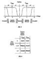
- the row/column actuation protocol may take advantage of a hysteresis property of these devices illustrated in Figure 3. It may require, for example, a 10 volt potential difference to cause a movable layer to deform from the relaxed state to the actuated state. However, when the voltage is reduced from that value, the movable layer maintains its state as the voltage drops back below 10 volts.
- the movable layer does not relax completely until the voltage drops below 2 volts.
- the row/column actuation protocol can be designed such that during row strobing, pixels in the strobed row that are to be actuated are exposed to a voltage difference of about 10 volts, and pixels that are to be relaxed are exposed to a voltage difference of close to zero volts.
- each pixel sees a potential difference within the "stability window" of 3-7 volts in this example.
- This feature makes the pixel design illustrated in Figure 1 stable under the same applied voltage conditions in either an actuated or relaxed pre-existing state. Since each pixel of the interferometric modulator, whether in the actuated or relaxed state, is essentially a capacitor formed by the fixed and moving reflective layers, this stable state can be held at a voltage within the hysteresis window with almost no power dissipation. Essentially no current flows into the pixel if the applied potential is fixed.
- a display frame may be created by asserting the set of column electrodes in accordance with the desired set of actuated pixels in the first row.
- a row pulse is then applied to the row 1 electrode, actuating the pixels corresponding to the asserted column lines.
- the asserted set of column electrodes is then changed to correspond to the desired set of actuated pixels in the second row.
- a pulse is then applied to the row 2 electrode, actuating the appropriate pixels in row 2 in accordance with the asserted column electrodes.
- the row I pixels are unaffected by the row 2 pulse, and remain in the state they were set to during the row 1 pulse. This may be repeated for the entire series of rows in a sequential fashion to produce the frame.
- the frames are refreshed and/or updated with new display data by continually repeating this process at some desired number of frames per second.
- protocols for driving row and column electrodes of pixel arrays to produce display frames are also well known and may be used in conjunction with the present invention.
- Figures 4, 5A, and 5B illustrate one possible actuation protocol for creating a display frame on the 3x3 array of Figure 2.
- Figure 4 illustrates a possible set of column and row voltage levels that may be used for pixels exhibiting the hysteresis curves of Figure 3.
- actuating a pixel involves setting the appropriate column to -V bias , and the appropriate row to + ⁇ V, which may correspond to -5 volts and +5 volts respectively Relaxing the pixel is accomplished by setting the appropriate column to +V bias , and the appropriate row to the same + ⁇ V, producing a zero volt potential difference across the pixel.
- the pixels are stable in whatever state they were originally in, regardless of whether the column is at +V bias , or -V bias .
- voltages of opposite polarity than those described above can be used, e.g., actuating a pixel can involve setting the appropriate column to +V bias , and the appropriate row to - ⁇ V.
- releasing the pixel is accomplished by setting the appropriate column to -V bias , and the appropriate row to the same - ⁇ V, producing a zero volt potential difference across the pixel.
- Figure 5B is a timing diagram showing a series of row and column signals applied to the 3x3 array of Figure 2 which will result in the display arrangement illustrated in Figure 5A, where actuated pixels are non-reflective.
- the pixels Prior to writing the frame illustrated in Figure 5A, the pixels can be in any state, and in this example, all the rows are at 0 volts, and all the columns are at +5 volts. With these applied voltages, all pixels are stable in their existing actuated or relaxed states.
- pixels (1,1), (1,2), (2,2), (3,2) and (3,3) are actuated.
- columns 1 and 2 are set to-5 volts, and column 3 is set to +5 volts. This does not change the state of any pixels, because all the pixels remain in the 3-7 volt stability window.
- Row 1 is then strobed with a pulse that goesfrom 0, up to 5 volts, and back to zero. This actuates the (1,1) and (1,2) pixels and relaxes the (1,3) pixel. No other pixels in the array are affected.
- column 2 is set to -5 volts
- columns 1 and 3 are set to +5 volts.
- Row 3 is similarly set by setting columns 2 and 3 to -5 volts, and column 1 to +5 volts.
- the row 3 strobe sets the row 3 pixels as shown in Figure 5A. After writing the frame, the row potentials are zero, and the column potentials can remain at either +5 or -5 volts, and the display is then stable in the arrangement of Figure 5A. It will be appreciated that the same procedure can be employed for arrays of dozens or hundreds of rows and columns.
- FIGS 6A and 6B are system block diagrams illustrating an embodiment of a display device 40.
- the display device 40 can be, for example, a cellular or mobile telephone.
- the same components of display device 40 or slight variations thereof are also illustrative of various types of display devices such as televisions and portable media players.
- the display device 40 includes a housing 41, a display 30, an antenna 43, a speaker 44, an input device 48, and a microphone 46.
- the housing 41 is generally formed from any of a variety of manufacturing processes as are well known to those of skill in the art, including injection molding, and vacuum forming.
- the housing 41 may be made from any of a variety of materials, including but not limited to plastic, metal, glass, rubber, and ceramic, or a combination thereof.
- the housing 41 includes removable portions (not shown) that may be interchanged with other removable portions of different color, or containing different logos, pictures, or symbols.
- the display 30 of exemplary display device 40 may be any of a variety of displays, including a bi-stable display, as described herein.
- the display 30 includes a flat-panel display, such as plasma, EL, OLED, STN LCD, or TFT LCD as described above, or a non-flat-panel display, such as a CRT or other tube device, as is well known to those of skill in the art.
- the display 30 includes an interferometric modulator display, as described herein.
- the components of one embodiment of exemplary display device 40 are schematically illustrated in Figure 6B.
- the illustrated exemplary display device 40 includes a housing 41 and can include additional components at least partially enclosed therein.
- the exemplary display device 40 includes a network interface 27 that includes an antenna 43 which is coupled to a transceiver 47.
- the transceiver 47 is connected to a processor 21, which is connected to conditioning hardware 52.
- the conditioning hardware 52 may be configured to condition a signal (e.g. filter a signal).
- the conditioning hardware 52 is connected to a speaker 44 and a microphone 46.
- the processor 21 is also connected to an input device 48 and a driver controller 29.
- the driver controller 29 is coupled to a frame buffer 28, and to an array driver 22, which in turn is coupled to a display array 30.
- a power supply 50 provides power to all components as required by the particular exemplary display device 40 design.
- the network interface 27 includes the antenna 43 and the transceiver 47 so that the exemplary display device 40 can communicate with one ore more devices over a network. In one embodiment the network interface 27 may also have some processing capabilities to relieve requirements of the processor 21.
- the antenna 43 is any antenna known to those of skill in the art for transmitting and receiving signals. In one embodiment, the antenna transmits and receives RF signals according to the IEEE 802.11 standard, including IEEE 802.11(a), (b), or (g). In another embodiment, the antenna transmits and receives RF signals according to the BLUETOOTH standard. In the case of a cellular telephone, the antenna is designed to receive CDMA, GSM, AMPS or other known signals that are used to communicate within a wireless cell phone network.
- the transceiver 47 pre-processes the signals received from the antenna 43 so that they may be received by and further manipulated by the processor 21.
- the transceiver 47 also processes signals received from the processor 21 so that they may be transmitted from the exemplary display device 40 via the antenna 43.
- the transceiver 47 can be replaced by a receiver.
- network interface 27 can be replaced by an image source, which can store or generate image data to be sent to the processor 21.
- the image source can be a digital video disc (DVD) or a hard-disc drive that contains image data, or a software module that generates image data.
- Processor 21 generally controls the overall operation of the exemplary display device 40.
- the processor 21 receives data, such as compressed image data from the network interface 27 or an image source, and processes the data into raw image data or into a format that is readily processed into raw image data.
- the processor 21 then sends the processed data to the driver controller 29 or to frame buffer 28 for storage.
- Raw data typically refers to the information that identifies the image characteristics at each location within an image. For example, such image characteristics can include color, saturation, and gray-scale level.
- the processor 21 includes a microcontroller, CPU, or logic unit to control operation of the exemplary display device 40.
- Conditioning hardware 52 generally includes amplifiers and filters for transmitting signals to the speaker 44, and for receiving signals from the microphone 46. Conditioning hardware 52 may be discrete components within the exemplary display device 40, or may be incorporated within the processor 21 or other components.
- the driver controller 29 takes the raw image data generated by the processor 21 either directly from the processor 21 or from the frame buffer 28 and reformats the raw image data appropriately for high speed transmission to the array driver 22. Specifically, the driver controller 29 reformats the raw image data into a data flow having a raster-like format, such that it has a time order suitable for scanning across the display array 30. Then the driver controller 29 sends the formatted information to the array driver 22.
- a driver controller 29, such as a LCD controller is often associated with the system processor 21 as a stand-alone Integrated Circuit (IC), such controllers may be implemented in many ways. They may be embedded in the processor 21 as hardware, embedded in the processor 21 as software, or fully integrated in hardware with the array driver 22.
- IC Integrated Circuit
- the array driver 22 receives the formatted information from the driver controller 29 and reformats the video data into a parallel set of waveforms that are applied many times per second to the hundreds and sometimes thousands of leads coming from the display's x-y matrix of pixels.
- driver controller 29 is a conventional display controller or a bi-stable display controller (e.g., an interferometric modulator controller).
- array driver 22 is a conventional driver or a bi-stable display driver (e.g., an interferometric modulator display).
- a driver controller 29 is integrated with the array driver 22.
- display array 30 is a typical display array or a bi-stable display array (e.g., a display including an array of interferometric modulators).
- the input device 48 allows a user to control the operation of the exemplary display device 40.
- input device 48 includes a keypad, such as a QWERTY keyboard or a telephone keypad, a button, a switch, a touch-sensitive screen, a pressure- or heat-sensitive membrane.
- the microphone 46 is an input device for the exemplary display device 40. When the microphone 46 is used to input data to the device, voice commands may be provided by a user for controlling operations of the exemplary display device 40.
- Power supply 50 can include a variety of energy storage devices as are well known in the art.
- power supply 50 is a rechargeable battery, such as a nickel-cadmium battery or a lithium ion battery.
- power supply 50 is a renewable energy source, a capacitor, or a solar cell, including a plastic solar cell, and solar-cell paint.
- power supply 50 is configured to receive power from a wall outlet.
- control programmability resides, as described above, in a driver controller which can be located in several places in the electronic display system. In some cases control programmability resides in the array driver 22. Those of skill in the art will recognize that the above-described optimization may be implemented in any number of hardware and/or software components and in various configurations.
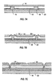
- Figures 7A-7C illustrate three different embodiments of the moving mirror structure.
- Figure 7A is a cross section of the embodiment of Figure 1, where a strip of metal material 14 is deposited on orthogonally extending supports 18.
- Figure 7B the moveable reflective material 14 is attached to supports at the corners only, on tethers 32.
- Figure 7C the moveable reflective material 14 is suspended from a deformable layer 34.
- This embodiment has benefits because the structural design and materials used for the reflective material 14 can be optimized with respect to the optical properties, and the structural design and materials used for the deformable layer 34 can be optimized with respect to desired mechanical properties.
- a MEMS device such as an interferometric modulator array
- the moving parts of a MEMS device preferably have a protected space in which to move.
- Packaging techniques for a MEMS device will be described in more detail below.
- a schematic of a basic package structure for a MEMS device, such as an interferometric modulator array, is illustrated in Figure 8.
- a basic package structure 70 includes a substrate 72 and a backplane cover or "cap" 74, wherein an interferometric modulator array 76 is formed on the substrate 72.
- This cap 74 is also called a "backplane".
- the substrate 72 and the backplane 74 are joined by a seal 78 to form the package structure 70, such that the interferometric modulator array 76 is encapsulated by the substrate 72, backplane 74, and the seal 78. This forms a cavity 79 between the backplane 74 and the substrate 72.
- the seal 78 may be a non-hermetic seal, such as a conventional epoxy-based adhesive.
- the seal 78 may be a polyisobutylene (sometimes called butyl rubber, and other times PIB), o-rings, polyurethane, thin film metal weld, liquid spin-on glass, solder, polymers, or plastics, among other types of seals that may have a range of permeability of water vapor of about 0.2 - 4.7 g mm/m2kPa day.
- the seal 78 may be a hermetic seal and may comprise, for example, metals, welds, and glass frits.
- Methods of hermetic sealing comprise, for example, metal or solder thin film or preforms, laser or resistive welding techniques, and anodic bonding techniques, wherein the resulting package structure may or may not require a desiccant to achieve the desired internal package requirements.
- the seal 78 may be implemented as a closed seal (continuous) or an open seal (non-continuous), and may be applied or formed on the substrate 72, backplane 74, or both the substrate and backplane 74 in a method of packaging the interferometric modulator array 76.
- the seal 78 may be applied through simple in-line manufacturing processes and may have advantages for lower temperature processes, whereas the techniques of welding and soldering may require very high temperature processes that can damage the package structure 20, are relatively expensive. In some cases, localized heating methods can be used to reduce the process temperatures and yield a viable process solution.
- the package structure 70 includes a getter such as a desiccant 80 configured to reduce moisture within the cavity 79.
- a desiccant may not be necessary for a hermetically sealed package, but may be desirable to control moisture resident within the package.
- the desiccant 80 is positioned between the interferometric modulator array 76 and the backplane 74.
- Desiccants may be used for packages that have either hermetic or non-hermetic seals. In packages having a hermetic seal, desiccants are typically used to control moisture resident within the interior of the package. In packages having a non-hermetic seal, a desiccant may be used to control moisture moving into the package from the environment.
- any substance that can trap moisture while not interfering with the optical properties of the interferometric modulator array may be used as the desiccant 80.
- Suitable getter and desiccant materials include, but are not limited to, zeolites, molecular sieves, surface adsorbents, bulk adsorbents, and chemical reactants.
- the desiccant 80 may be in different forms, shapes, and sizes. In addition to being in solid form, the desiccant 80 may alternatively be in powder form. These powders may be inserted directly into the package or they may be mixed with an adhesive for application. In an alternative embodiment, the desiccant 80 may be formed into different shapes, such as cylinders, rings, or sheets, before being applied inside the package.
- the desiccant 80 can be applied in different ways.
- the desiccant 80 is deposited as part of the interferometric modulator array 76.
- the desiccant 80 is applied inside the package 70 as a spray or a dip coat.
- the substrate 72 may be a semi-transparent or transparent substance capable of having thin film, MEMS devices built upon it. Such transparent substances include, but are not limited to, glass, plastic, and transparent polymers.
- the interferometric modulator array 76 may comprise membrane modulators or modulators of the separable type.
- the backplane 74 may be formed of any suitable material, such as glass, metal, foil, polymer, plastic, ceramic, or semiconductor materials (e.g., silicon).
- the packaging process may be accomplished in a vacuum, pressure between a vacuum up to and including ambient pressure, normal atmospheric pressure conditions, or pressure higher than ambient pressure.
- the packaging process may also be accomplished in an environment of varied and controlled high or low pressure during the sealing process.
- the packaging environment may be of an inert gas at ambient conditions. Packaging at ambient conditions allows for a lower cost process and more potential for versatility in equipment choice because the device may be transported through ambient conditions without affecting the operation of the device.
- MEMS devices such as interferometric modulator displays
- the lifetime of an interferometric modulator display may be determined based at least in part on the level of moisture control provided by the desiccant within a package structure and the water vapor permeability of the seal between the backplane and the substrate.
- the lifetime of a display device can be defined as the time at which the desiccant is saturated with water.
- the water saturating the desiccant includes the water vapor that naturally enters the package structure through the seal and is absorbed into the desiccant.
- the value can be designed to be very low, such as on the order of 0.0001 grams per day, such that the lifetime is on the order of about 10 years or more.
- the seal material may be selected according to its water vapor permeability properties depending on the expected lifetime of the interferometric modulator display.
- an interferometric modulator display intended for use in inexpensive and/or disposable devices, such as children's toys and disposable cameras, may comprise a seal with a higher water vapor permeability rate than a device intended to have a longer lifetime.
- Figure 9 is a side-view illustration of one embodiment of the package structure 70 including a secondary seal 82.
- the secondary seal 82 is formed or positioned substantially around the perimeter of the backplane 74 and the outer periphery of the primary seal 48, and in contact with the substrate 72, thereby sealing the junction of the backplane 74, primary seal 48, and the substrate 72 from ambient conditions.
- the secondary seal 82 may be formed as a fillet, or have a plurality of different cross-sectional geometries, such as circular, ovular, or rectangular.
- the secondary seal 82 may comprise a non-hermetic seal, such as a conventional epoxy-based adhesive or silicone based adhesive.
- the secondary seal 82 comprises PIB (polyisobutylene), a UV curable adhesive, one or more o-rings, polyurethane, thin film metal weld, liquid spin-on glass, solder (such as a solder preform), polymers, plastics, or hydrophobic film or liquid, or a combination thereof.
- the secondary seal 82 may be a hermetic seal.
- the outer seal provides a means for sealing the outer periphery of the primary seal.
- the secondary seal 82 may be formed or applied to the package structure through a plurality of methods, such as application in a liquid or semi-liquid state and curing through exposure to air, elevated temperatures, UV light, and/or placement. Exemplary methods of forming and placing a secondary seal are discussed in more detail hereinafter in reference to Figures 9 and 11.
- the combined water vapor permeability of the secondary seal 82 and the primary seal 78 accords with a desired total water vapor permeability for the package structure 70.
- a material with a higher water vapor permeability coefficient and lower effective lifetime than the primary seal may be used for the secondary seal 82.
- the addition of the secondary seal 82 provides for relaxed constraints on the properties of the primary seal 78, thereby reducing testing procedures and costs in optimization of the primary seal 78.
- the package structure for interferometric modulator displays intended for short use for example, such as in inexpensive and/or disposable devices, can be modified to reduce material reliability constraints. Relaxed constraints on the properties of the package structure seal can reduce costs for the package structure, thereby making the implementation of interferometric modulator displays in short use devices cost effective.
- FIG. 10 is a flow diagram illustrating one embodiment of a method 900 of sealing a MEMS device, such as an interferometric modulator device, package with a secondary seal.
- the method 900 begins in a step 902 and proceeds to a step 904 wherein a solder preform is placed on a substrate proximate to a perimeter of a MEMS device formed on the substrate.
- the solder preform may comprise, for example, lead or tin.
- the method proceeds to a step 906 wherein a primary seal, the substrate, and a backplane are contacted so as to seal the MEMS device from ambient conditions.
- the primary seal preferably contacts the substrate between the MEMS device formed thereon and the solder preform, and the primary seal may be initially positioned on the substrate, the backplane, or both the substrate and the backplane.
- the method 900 proceeds to a step 908 wherein the solder preform is melted so as to contact the backplane and form a secondary seal in contact with the substrate and the backplane. The solder may also be melted so as to contact the primary seal.
- the method ends in a step 910.
- the solder preform is placed on the substrate after the primary seal, substrate, and backplane are contacted.
- contacting the primary seal, substrate, and backplane in step 906 functions primarily to align and/or affix the backplane with the substrate, wherein, for example, the primary seal comprises an adhesive.
- the secondary seal formed from the solder preform may then function as the major environmental seal for the device package, wherein the primary seal provides minor sealant attributes to the device package.
- FIG 11 is a side-view illustration of another embodiment of an interferometric modulator display package structure 70 with a secondary seal.
- the position of the movable layer of each element of the interferometric modulator array is controlled by the application of a voltage across the two layers which form the cavity.
- each interferometric modulator array element is coupled to conductive leads 1002 on the substrate 72, and the conductive leads 1002 are coupled to a driver circuit 1004 configured to control the voltage applied to each interferometric modulator array element, such as the array driver 22.
- the driver circuit 1004 is coupled to the conductive leads 1004 at a perimeter of the substrate 72 via a flexible circuit or conductive tape 1006 and an anisotropic conductive film (ACF) 1008.
- ACF comprises a thermoset adhesive binder and a matrix of conductive particles or spheres 1010.
- the flexible circuit 1006 typically includes a plurality of conductive leads, which are electrically coupled to the conductive leads 1002 on the substrate 72 via the conductive particles 1010 in the ACF 1008.
- the ACF adhesive is in a solid state (or semi-solid state) and may be applied in a tape form.
- the ACF melts with the application of an elevated temperature and subsequently solidifies when cooled to room temperature. Accordingly, the final position of the ACF can be manipulated by applying pressure to the flexible circuit 1006 to force a quantity or portion of the ACF 1008 to contact the backplane 74, thereby forming a secondary seal in contact with the backplane 74 and the substrate 72.
- the ACF 1008 is also in contact with the primary seal.
- the secondarily sealed interferometric modulator device package structure of Figure 11 advantageously includes improved seal properties without additional material cost or assembly/manufacturing processes for a second seal.
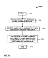
- a method 1100 of sealing an interferometric modulator array package structure with a secondary seal is illustrated in the flow diagram of Figure 12.
- the method 1100 begins in a step 1102 and proceeds to a step 1104 wherein a primary seal is provided between a backplane and a substrate, wherein a MEMS device, such as an interferometric modulator device, is formed on the substrate.
- the method further comprises contacting an ACF to conductive leads on the substrate in a step 1106, wherein the ACF provides electrical connection between the conductive leads on the substrate and a flexible circuit.
- the flexible circuit can be configured for connection to an array driver circuit, for example.
- the method proceeds to a step 1108 wherein a force is applied to the flexible circuit sufficient to force a portion of the ACF in contact with the package backplane and primary seal.
- the ACF is in contact with only the substrate and the backplane, and not the primary seal.
- the method 1100 additionally comprises forming a third seal or barrier, such as a hydrophobic seal, on the ACF, thereby further reducing the water permeability of the package structure.
- the ACF may comprise a sealing region wherein a portion of the ACF is specifically tailored for sealing.
- the material at the sealing region of the ACF may comprise both a resin and conductive particles, wherein the resin is configured with a hydrophobic property or highly water impermeable barrier for implementation as a secondary seal.
- the secondary seal may have a plurality of forms and configurations, and may comprise a plurality of materials.
- the methods of formation of the secondary seal may include more or fewer steps, and may, for example take place before, during, or after encapsulation of a MEMS device within a packaging structure.
Landscapes
- Engineering & Computer Science (AREA)
- Microelectronics & Electronic Packaging (AREA)
- Computer Hardware Design (AREA)
- Mechanical Light Control Or Optical Switches (AREA)
- Micromachines (AREA)
- Pressure Sensors (AREA)
- Structures Or Materials For Encapsulating Or Coating Semiconductor Devices Or Solid State Devices (AREA)
- Vacuum Packaging (AREA)
- Devices For Indicating Variable Information By Combining Individual Elements (AREA)
Applications Claiming Priority (2)
| Application Number | Priority Date | Filing Date | Title |
|---|---|---|---|
| US61352704P | 2004-09-27 | 2004-09-27 | |
| US11/134,838 US20060076631A1 (en) | 2004-09-27 | 2005-05-20 | Method and system for providing MEMS device package with secondary seal |
Publications (2)
| Publication Number | Publication Date |
|---|---|
| EP1640326A2 true EP1640326A2 (de) | 2006-03-29 |
| EP1640326A3 EP1640326A3 (de) | 2008-04-02 |
Family
ID=35207576
Family Applications (1)
| Application Number | Title | Priority Date | Filing Date |
|---|---|---|---|
| EP05255660A Withdrawn EP1640326A3 (de) | 2004-09-27 | 2005-09-14 | Methode und System, um ein Gehäuse für ein MEMS-Bauteil mit einer zusätzlichen Dichtung zu versehen |
Country Status (11)
| Country | Link |
|---|---|
| US (1) | US20060076631A1 (de) |
| EP (1) | EP1640326A3 (de) |
| JP (1) | JP2006123160A (de) |
| KR (1) | KR20060092916A (de) |
| AU (1) | AU2005204263A1 (de) |
| BR (1) | BRPI0503900A (de) |
| CA (1) | CA2519484A1 (de) |
| MX (1) | MXPA05010088A (de) |
| RU (1) | RU2005129980A (de) |
| SG (1) | SG121148A1 (de) |
| TW (1) | TW200627603A (de) |
Cited By (3)
| Publication number | Priority date | Publication date | Assignee | Title |
|---|---|---|---|---|
| EP1890180A1 (de) * | 2006-08-15 | 2008-02-20 | STMicroelectronics (Research & Development) Limited | Optisches Modul |
| WO2007149475A3 (en) * | 2006-06-21 | 2008-06-05 | Qualcomm Mems Technologies Inc | Method for packaging an optical mems device |
| WO2008021227A3 (en) * | 2006-08-15 | 2008-06-12 | Qualcomm Mems Technologies Inc | High profile contacts for microelectromechanical systems |
Families Citing this family (21)
| Publication number | Priority date | Publication date | Assignee | Title |
|---|---|---|---|---|
| TWI289708B (en) | 2002-12-25 | 2007-11-11 | Qualcomm Mems Technologies Inc | Optical interference type color display |
| US7342705B2 (en) | 2004-02-03 | 2008-03-11 | Idc, Llc | Spatial light modulator with integrated optical compensation structure |
| US7405924B2 (en) * | 2004-09-27 | 2008-07-29 | Idc, Llc | System and method for protecting microelectromechanical systems array using structurally reinforced back-plate |
| US7968426B1 (en) * | 2005-10-24 | 2011-06-28 | Microwave Bonding Instruments, Inc. | Systems and methods for bonding semiconductor substrates to metal substrates using microwave energy |
| US7561334B2 (en) * | 2005-12-20 | 2009-07-14 | Qualcomm Mems Technologies, Inc. | Method and apparatus for reducing back-glass deflection in an interferometric modulator display device |
| US7746537B2 (en) | 2006-04-13 | 2010-06-29 | Qualcomm Mems Technologies, Inc. | MEMS devices and processes for packaging such devices |
| FR2901639B1 (fr) * | 2006-05-24 | 2008-08-22 | Commissariat Energie Atomique | Micro-composant integre associant les fonctions de recuperation et de stockage de l'energie |
| EP1943551A2 (de) | 2006-10-06 | 2008-07-16 | Qualcomm Mems Technologies, Inc. | Lichtführung |
| ATE556272T1 (de) | 2006-10-06 | 2012-05-15 | Qualcomm Mems Technologies Inc | Optische verluststruktur in einer beleuchtungsvorrichtung |
| WO2009041950A1 (en) * | 2007-09-28 | 2009-04-02 | Qualcomm Mems Technologies, Inc. | Method of manufacturing a mems package using partially reactivated desiccant |
| FR2922203B1 (fr) * | 2007-10-15 | 2009-11-20 | Commissariat Energie Atomique | Procede de realisation d'une structure ayant un cordon de scellement ajoure et structure obtenue. |
| US8068710B2 (en) * | 2007-12-07 | 2011-11-29 | Qualcomm Mems Technologies, Inc. | Decoupled holographic film and diffuser |
| US20090323170A1 (en) * | 2008-06-30 | 2009-12-31 | Qualcomm Mems Technologies, Inc. | Groove on cover plate or substrate |
| US20100020382A1 (en) * | 2008-07-22 | 2010-01-28 | Qualcomm Mems Technologies, Inc. | Spacer for mems device |
| US8379392B2 (en) * | 2009-10-23 | 2013-02-19 | Qualcomm Mems Technologies, Inc. | Light-based sealing and device packaging |
| US9090456B2 (en) * | 2009-11-16 | 2015-07-28 | Qualcomm Mems Technologies, Inc. | System and method of manufacturing an electromechanical device by printing raised conductive contours |
| US20130050155A1 (en) * | 2011-08-30 | 2013-02-28 | Qualcomm Mems Technologies, Inc. | Glass as a substrate material and a final package for mems and ic devices |
| JP6244616B2 (ja) * | 2012-08-30 | 2017-12-13 | セイコーエプソン株式会社 | 波長可変干渉フィルター、光学モジュール、電子機器、および波長可変干渉フィルターの製造方法 |
| JP6260080B2 (ja) | 2013-01-07 | 2018-01-17 | セイコーエプソン株式会社 | 波長可変干渉フィルター、波長可変干渉フィルターの製造方法、光学モジュール、及び電子機器 |
| US10145739B2 (en) | 2014-04-03 | 2018-12-04 | Oto Photonics Inc. | Waveguide sheet, fabrication method thereof and spectrometer using the same |
| CN109830850B (zh) * | 2019-03-29 | 2024-04-19 | 四川华丰科技股份有限公司 | 用于高速连接器的模块结构及高速连接器 |
Family Cites Families (69)
| Publication number | Priority date | Publication date | Assignee | Title |
|---|---|---|---|---|
| US40436A (en) * | 1863-10-27 | Improvement in fruit-baskets | ||
| US3704806A (en) * | 1971-01-06 | 1972-12-05 | Le T Im Lensoveta | Dehumidifying composition and a method for preparing the same |
| JPS5836030B2 (ja) * | 1972-11-02 | 1983-08-06 | 株式会社クラレ | セツチヤクザイソセイブツ |
| JPS5918136A (ja) * | 1982-07-16 | 1984-01-30 | Toyota Central Res & Dev Lab Inc | 断熱被覆発泡ガラス成形体 |
| US4950344A (en) * | 1988-12-05 | 1990-08-21 | Lauren Manufacturing Company | Method of manufacturing multiple-pane sealed glazing units |
| US5095375A (en) * | 1991-03-29 | 1992-03-10 | Hughes Aircraft Company | Holographic combiner edge seal design and composition |
| US5212582A (en) * | 1992-03-04 | 1993-05-18 | Texas Instruments Incorporated | Electrostatically controlled beam steering device and method |
| US5293511A (en) * | 1993-03-16 | 1994-03-08 | Texas Instruments Incorporated | Package for a semiconductor device |
| US6674562B1 (en) * | 1994-05-05 | 2004-01-06 | Iridigm Display Corporation | Interferometric modulation of radiation |
| US5559358A (en) * | 1993-05-25 | 1996-09-24 | Honeywell Inc. | Opto-electro-mechanical device or filter, process for making, and sensors made therefrom |
| AU676299B2 (en) * | 1993-06-28 | 1997-03-06 | Akira Fujishima | Photocatalyst composite and process for producing the same |
| US7138984B1 (en) * | 2001-06-05 | 2006-11-21 | Idc, Llc | Directly laminated touch sensitive screen |
| US6680792B2 (en) * | 1994-05-05 | 2004-01-20 | Iridigm Display Corporation | Interferometric modulation of radiation |
| US6040937A (en) * | 1994-05-05 | 2000-03-21 | Etalon, Inc. | Interferometric modulation |
| US20010003487A1 (en) * | 1996-11-05 | 2001-06-14 | Mark W. Miles | Visible spectrum modulator arrays |
| US7123216B1 (en) * | 1994-05-05 | 2006-10-17 | Idc, Llc | Photonic MEMS and structures |
| US5553440A (en) * | 1994-10-20 | 1996-09-10 | Ppg Industries, Inc. | Multi-sheet glazing unit and method of making same |
| US5550373A (en) * | 1994-12-30 | 1996-08-27 | Honeywell Inc. | Fabry-Perot micro filter-detector |
| US6388203B1 (en) * | 1995-04-04 | 2002-05-14 | Unitive International Limited | Controlled-shaped solder reservoirs for increasing the volume of solder bumps, and structures formed thereby |
| US6969635B2 (en) * | 2000-12-07 | 2005-11-29 | Reflectivity, Inc. | Methods for depositing, releasing and packaging micro-electromechanical devices on wafer substrates |
| US5851609A (en) * | 1996-02-27 | 1998-12-22 | Truseal Technologies, Inc. | Preformed flexible laminate |
| US5939785A (en) * | 1996-04-12 | 1999-08-17 | Texas Instruments Incorporated | Micromechanical device including time-release passivant |
| DE19824965A1 (de) * | 1998-06-04 | 1999-12-09 | Metallgesellschaft Ag | Schmelzklebstoff zur Randabdichtung von Verbundglas, Verfahren zur Herstellung des Schmelzklebstoffs und seine Verwendung |
| US6872984B1 (en) * | 1998-07-29 | 2005-03-29 | Silicon Light Machines Corporation | Method of sealing a hermetic lid to a semiconductor die at an angle |
| JP2000058593A (ja) * | 1998-08-03 | 2000-02-25 | Nec Corp | 表面弾性波素子の実装構造及びその実装方法 |
| JP4336427B2 (ja) * | 1999-10-01 | 2009-09-30 | 帝人株式会社 | 表面保護フィルムおよびそれからなる積層体 |
| US6452238B1 (en) * | 1999-10-04 | 2002-09-17 | Texas Instruments Incorporated | MEMS wafer level package |
| US6400009B1 (en) * | 1999-10-15 | 2002-06-04 | Lucent Technologies Inc. | Hermatic firewall for MEMS packaging in flip-chip bonded geometry |
| US6521477B1 (en) * | 2000-02-02 | 2003-02-18 | Raytheon Company | Vacuum package fabrication of integrated circuit components |
| US6384473B1 (en) * | 2000-05-16 | 2002-05-07 | Sandia Corporation | Microelectronic device package with an integral window |
| US6661084B1 (en) * | 2000-05-16 | 2003-12-09 | Sandia Corporation | Single level microelectronic device package with an integral window |
| US6762868B2 (en) * | 2000-11-16 | 2004-07-13 | Texas Instruments Incorporated | Electro-optical package with drop-in aperture |
| US6664779B2 (en) * | 2000-11-16 | 2003-12-16 | Texas Instruments Incorporated | Package with environmental control material carrier |
| US20020075551A1 (en) * | 2000-11-29 | 2002-06-20 | Onix Microsystems, Inc | Enclosure for MEMS apparatus and method of using the same |
| US6906847B2 (en) * | 2000-12-07 | 2005-06-14 | Reflectivity, Inc | Spatial light modulators with light blocking/absorbing areas |
| US7307775B2 (en) * | 2000-12-07 | 2007-12-11 | Texas Instruments Incorporated | Methods for depositing, releasing and packaging micro-electromechanical devices on wafer substrates |
| US7123026B2 (en) * | 2001-01-23 | 2006-10-17 | Nippon Telegraph And Telephone Corporation | Surface shape recognition sensor and method of manufacturing the same |
| US6455927B1 (en) * | 2001-03-12 | 2002-09-24 | Amkor Technology, Inc. | Micromirror device package |
| KR100387239B1 (ko) * | 2001-04-26 | 2003-06-12 | 삼성전자주식회사 | Mems 릴레이 및 그 제조방법 |
| US6706316B2 (en) * | 2001-05-08 | 2004-03-16 | Eastman Kodak Company | Ultrasonically sealing the cover plate to provide a hermetic enclosure for OLED displays |
| US6589625B1 (en) * | 2001-08-01 | 2003-07-08 | Iridigm Display Corporation | Hermetic seal and method to create the same |
| US6940636B2 (en) * | 2001-09-20 | 2005-09-06 | Analog Devices, Inc. | Optical switching apparatus and method of assembling same |
| US6893574B2 (en) * | 2001-10-23 | 2005-05-17 | Analog Devices Inc | MEMS capping method and apparatus |
| KR100442830B1 (ko) * | 2001-12-04 | 2004-08-02 | 삼성전자주식회사 | 저온의 산화방지 허메틱 실링 방법 |
| US6776538B2 (en) * | 2001-12-12 | 2004-08-17 | Axsun Technologies, Inc. | MEMS tunable optical filter system with moisture getter for frequency stability |
| US6791660B1 (en) * | 2002-02-12 | 2004-09-14 | Seiko Epson Corporation | Method for manufacturing electrooptical device and apparatus for manufacturing the same, electrooptical device and electronic appliances |
| US7045459B2 (en) * | 2002-02-19 | 2006-05-16 | Northrop Grumman Corporation | Thin film encapsulation of MEMS devices |
| US6603182B1 (en) * | 2002-03-12 | 2003-08-05 | Lucent Technologies Inc. | Packaging micromechanical devices |
| US6838309B1 (en) * | 2002-03-13 | 2005-01-04 | Amkor Technology, Inc. | Flip-chip micromachine package using seal layer |
| US6707351B2 (en) * | 2002-03-27 | 2004-03-16 | Motorola, Inc. | Tunable MEMS resonator and method for tuning |
| US20030183916A1 (en) * | 2002-03-27 | 2003-10-02 | John Heck | Packaging microelectromechanical systems |
| US7034984B2 (en) * | 2002-06-19 | 2006-04-25 | Miradia Inc. | Fabrication of a high fill ratio reflective spatial light modulator with hidden hinge |
| US20040048027A1 (en) * | 2002-09-06 | 2004-03-11 | Hayes Michael W. | Honeycomb cores for aerospace applications |
| US7388631B2 (en) * | 2002-10-10 | 2008-06-17 | Samsung Electronics, Co., Ltd. | Parallax compensating color filter and black mask for display apparatus |
| US7071594B1 (en) * | 2002-11-04 | 2006-07-04 | Microvision, Inc. | MEMS scanner with dual magnetic and capacitive drive |
| US20040140557A1 (en) * | 2003-01-21 | 2004-07-22 | United Test & Assembly Center Limited | Wl-bga for MEMS/MOEMS devices |
| TW591778B (en) * | 2003-03-18 | 2004-06-11 | Advanced Semiconductor Eng | Package structure for a microsystem |
| US7015885B2 (en) * | 2003-03-22 | 2006-03-21 | Active Optical Networks, Inc. | MEMS devices monolithically integrated with drive and control circuitry |
| TWI251712B (en) * | 2003-08-15 | 2006-03-21 | Prime View Int Corp Ltd | Interference display plate |
| TWI305599B (en) * | 2003-08-15 | 2009-01-21 | Qualcomm Mems Technologies Inc | Interference display panel and method thereof |
| TW593127B (en) * | 2003-08-18 | 2004-06-21 | Prime View Int Co Ltd | Interference display plate and manufacturing method thereof |
| JP3979982B2 (ja) * | 2003-08-29 | 2007-09-19 | シャープ株式会社 | 干渉性変調器および表示装置 |
| TWI232333B (en) * | 2003-09-03 | 2005-05-11 | Prime View Int Co Ltd | Display unit using interferometric modulation and manufacturing method thereof |
| US7012726B1 (en) * | 2003-11-03 | 2006-03-14 | Idc, Llc | MEMS devices with unreleased thin film components |
| US7119945B2 (en) * | 2004-03-03 | 2006-10-10 | Idc, Llc | Altering temporal response of microelectromechanical elements |
| US7164520B2 (en) * | 2004-05-12 | 2007-01-16 | Idc, Llc | Packaging for an interferometric modulator |
| US20050253283A1 (en) * | 2004-05-13 | 2005-11-17 | Dcamp Jon B | Getter deposition for vacuum packaging |
| US7126741B2 (en) * | 2004-08-12 | 2006-10-24 | Hewlett-Packard Development Company, L.P. | Light modulator assembly |
| US7327510B2 (en) * | 2004-09-27 | 2008-02-05 | Idc, Llc | Process for modifying offset voltage characteristics of an interferometric modulator |
-
2005
- 2005-05-20 US US11/134,838 patent/US20060076631A1/en not_active Abandoned
- 2005-08-26 AU AU2005204263A patent/AU2005204263A1/en not_active Abandoned
- 2005-08-29 TW TW094129533A patent/TW200627603A/zh unknown
- 2005-09-14 EP EP05255660A patent/EP1640326A3/de not_active Withdrawn
- 2005-09-14 CA CA002519484A patent/CA2519484A1/en not_active Abandoned
- 2005-09-16 SG SG200505988A patent/SG121148A1/en unknown
- 2005-09-21 MX MXPA05010088A patent/MXPA05010088A/es not_active Application Discontinuation
- 2005-09-26 RU RU2005129980/28A patent/RU2005129980A/ru not_active Application Discontinuation
- 2005-09-27 JP JP2005279055A patent/JP2006123160A/ja active Pending
- 2005-09-27 KR KR1020050089830A patent/KR20060092916A/ko not_active Withdrawn
- 2005-09-27 BR BRPI0503900-2A patent/BRPI0503900A/pt not_active Application Discontinuation
Cited By (5)
| Publication number | Priority date | Publication date | Assignee | Title |
|---|---|---|---|---|
| WO2007149475A3 (en) * | 2006-06-21 | 2008-06-05 | Qualcomm Mems Technologies Inc | Method for packaging an optical mems device |
| US7826127B2 (en) | 2006-06-21 | 2010-11-02 | Qualcomm Mems Technologies, Inc. | MEMS device having a recessed cavity and methods therefor |
| EP1890180A1 (de) * | 2006-08-15 | 2008-02-20 | STMicroelectronics (Research & Development) Limited | Optisches Modul |
| WO2008021227A3 (en) * | 2006-08-15 | 2008-06-12 | Qualcomm Mems Technologies Inc | High profile contacts for microelectromechanical systems |
| US7672060B2 (en) | 2006-08-15 | 2010-03-02 | Stmicroelectronics (Research & Development) Limited | Lens unit |
Also Published As
| Publication number | Publication date |
|---|---|
| KR20060092916A (ko) | 2006-08-23 |
| US20060076631A1 (en) | 2006-04-13 |
| CA2519484A1 (en) | 2006-03-27 |
| EP1640326A3 (de) | 2008-04-02 |
| AU2005204263A1 (en) | 2006-04-13 |
| MXPA05010088A (es) | 2006-04-27 |
| SG121148A1 (en) | 2006-04-26 |
| BRPI0503900A (pt) | 2006-05-09 |
| TW200627603A (en) | 2006-08-01 |
| JP2006123160A (ja) | 2006-05-18 |
| RU2005129980A (ru) | 2007-04-10 |
Similar Documents
| Publication | Publication Date | Title |
|---|---|---|
| EP1640326A2 (de) | Methode und System, um ein Gehäuse für ein MEMS-Bauteil mit einer zusätzlichen Dichtung zu versehen | |
| EP1640323A2 (de) | System und Verfahren für eine Anzeigevorrichtung mit aktiviertem Trocknungsmittel | |
| EP1640327A2 (de) | Verfahren und System zum Verkapseln von MEMS-Vorrichtungen mit integriertem Getter | |
| US7715080B2 (en) | Packaging a MEMS device using a frame | |
| US8040587B2 (en) | Desiccant in a MEMS device | |
| US7746539B2 (en) | Method for packing a display device and the device obtained thereof | |
| EP1640324A2 (de) | System und Methode für eine Anzeigevorrichtung mit integriertem Trockenmittel | |
| EP1655720A2 (de) | Elektronische Anzeige und Verfahren zu deren Herstellung | |
| EP1640772A1 (de) | System und Verfahren zur Herstellung eines MEMS - Bauelementes mit Antihaftbeschichtung | |
| JP4331148B2 (ja) | 基板を封止するための方法およびシステム | |
| EP1640320A2 (de) | Methode und Aufbau zur Häusung einer mikromechanischen Anzeigevorrichtung | |
| WO2007149475A2 (en) | Method for packaging an optical mems device | |
| EP1640330A2 (de) | Methode und Vorrichtung zur Häusung eines Substrats | |
| EP1640332A2 (de) | System und Verfahren für eine Anzeigevorrichtung mit Effekt am Ende der Lebensdauer | |
| US7550912B2 (en) | Method and system for maintaining partial vacuum in display device | |
| HK1087785A (en) | Method and system for providing mems device package with secondary seal |
Legal Events
| Date | Code | Title | Description |
|---|---|---|---|
| PUAI | Public reference made under article 153(3) epc to a published international application that has entered the european phase |
Free format text: ORIGINAL CODE: 0009012 |
|
| AK | Designated contracting states |
Kind code of ref document: A2 Designated state(s): AT BE BG CH CY CZ DE DK EE ES FI FR GB GR HU IE IS IT LI LT LU LV MC NL PL PT RO SE SI SK TR |
|
| AX | Request for extension of the european patent |
Extension state: AL BA HR MK YU |
|
| PUAL | Search report despatched |
Free format text: ORIGINAL CODE: 0009013 |
|
| AK | Designated contracting states |
Kind code of ref document: A3 Designated state(s): AT BE BG CH CY CZ DE DK EE ES FI FR GB GR HU IE IS IT LI LT LU LV MC NL PL PT RO SE SI SK TR |
|
| AX | Request for extension of the european patent |
Extension state: AL BA HR MK YU |
|
| RIC1 | Information provided on ipc code assigned before grant |
Ipc: H01L 23/10 20060101ALI20080226BHEP Ipc: G02B 26/08 20060101ALI20080226BHEP Ipc: B81B 7/00 20060101AFI20051110BHEP |
|
| AKX | Designation fees paid | ||
| REG | Reference to a national code |
Ref country code: DE Ref legal event code: 8566 |
|
| 17P | Request for examination filed |
Effective date: 20090122 |
|
| RBV | Designated contracting states (corrected) |
Designated state(s): AT BE BG CH CY CZ DE DK EE ES FI FR GB GR HU IE IS IT LI LT LU LV MC NL PL PT RO SE SI SK TR |
|
| 17Q | First examination report despatched |
Effective date: 20090225 |
|
| STAA | Information on the status of an ep patent application or granted ep patent |
Free format text: STATUS: THE APPLICATION IS DEEMED TO BE WITHDRAWN |
|
| 18D | Application deemed to be withdrawn |
Effective date: 20090708 |