EP1640733B1 - Procédé et dispositif pour la mesure de la phase d'un signal - Google Patents
Procédé et dispositif pour la mesure de la phase d'un signal Download PDFInfo
- Publication number
- EP1640733B1 EP1640733B1 EP04292278A EP04292278A EP1640733B1 EP 1640733 B1 EP1640733 B1 EP 1640733B1 EP 04292278 A EP04292278 A EP 04292278A EP 04292278 A EP04292278 A EP 04292278A EP 1640733 B1 EP1640733 B1 EP 1640733B1
- Authority
- EP
- European Patent Office
- Prior art keywords
- frequency
- phase
- sampling
- signal
- counter
- Prior art date
- Legal status (The legal status is an assumption and is not a legal conclusion. Google has not performed a legal analysis and makes no representation as to the accuracy of the status listed.)
- Expired - Lifetime
Links
- 238000000034 method Methods 0.000 title claims abstract description 44
- 238000005070 sampling Methods 0.000 claims abstract description 81
- 230000005540 biological transmission Effects 0.000 claims abstract description 18
- 230000001360 synchronised effect Effects 0.000 claims description 32
- 238000001914 filtration Methods 0.000 claims description 12
- 230000008569 process Effects 0.000 claims description 4
- 238000005259 measurement Methods 0.000 description 21
- 230000000737 periodic effect Effects 0.000 description 18
- 230000003595 spectral effect Effects 0.000 description 7
- 230000008929 regeneration Effects 0.000 description 5
- 238000011069 regeneration method Methods 0.000 description 5
- 230000007704 transition Effects 0.000 description 4
- 230000000630 rising effect Effects 0.000 description 3
- 230000001419 dependent effect Effects 0.000 description 2
- 230000000694 effects Effects 0.000 description 2
- RGNPBRKPHBKNKX-UHFFFAOYSA-N hexaflumuron Chemical compound C1=C(Cl)C(OC(F)(F)C(F)F)=C(Cl)C=C1NC(=O)NC(=O)C1=C(F)C=CC=C1F RGNPBRKPHBKNKX-UHFFFAOYSA-N 0.000 description 2
- 230000003247 decreasing effect Effects 0.000 description 1
- 230000008713 feedback mechanism Effects 0.000 description 1
- 230000010354 integration Effects 0.000 description 1
- 238000013507 mapping Methods 0.000 description 1
- 230000010355 oscillation Effects 0.000 description 1
- 229920000729 poly(L-lysine) polymer Polymers 0.000 description 1
- 230000001902 propagating effect Effects 0.000 description 1
- 238000011084 recovery Methods 0.000 description 1
- 230000001172 regenerating effect Effects 0.000 description 1
Images



Classifications
-
- G—PHYSICS
- G01—MEASURING; TESTING
- G01R—MEASURING ELECTRIC VARIABLES; MEASURING MAGNETIC VARIABLES
- G01R25/00—Arrangements for measuring phase angle between a voltage and a current or between voltages or currents
- G01R25/08—Arrangements for measuring phase angle between a voltage and a current or between voltages or currents by counting of standard pulses
-
- G—PHYSICS
- G01—MEASURING; TESTING
- G01R—MEASURING ELECTRIC VARIABLES; MEASURING MAGNETIC VARIABLES
- G01R25/00—Arrangements for measuring phase angle between a voltage and a current or between voltages or currents
- G01R25/005—Circuits for comparing several input signals and for indicating the result of this comparison, e.g. equal, different, greater, smaller, or for passing one of the input signals as output signal
-
- H—ELECTRICITY
- H03—ELECTRONIC CIRCUITRY
- H03L—AUTOMATIC CONTROL, STARTING, SYNCHRONISATION OR STABILISATION OF GENERATORS OF ELECTRONIC OSCILLATIONS OR PULSES
- H03L7/00—Automatic control of frequency or phase; Synchronisation
- H03L7/06—Automatic control of frequency or phase; Synchronisation using a reference signal applied to a frequency- or phase-locked loop
- H03L7/08—Details of the phase-locked loop
- H03L7/085—Details of the phase-locked loop concerning mainly the frequency- or phase-detection arrangement including the filtering or amplification of its output signal
- H03L7/091—Details of the phase-locked loop concerning mainly the frequency- or phase-detection arrangement including the filtering or amplification of its output signal the phase or frequency detector using a sampling device
-
- H—ELECTRICITY
- H04—ELECTRIC COMMUNICATION TECHNIQUE
- H04J—MULTIPLEX COMMUNICATION
- H04J3/00—Time-division multiplex systems
- H04J3/16—Time-division multiplex systems in which the time allocation to individual channels within a transmission cycle is variable, e.g. to accommodate varying complexity of signals, to vary number of channels transmitted
- H04J3/1605—Fixed allocated frame structures
- H04J3/1611—Synchronous digital hierarchy [SDH] or SONET
-
- H—ELECTRICITY
- H04—ELECTRIC COMMUNICATION TECHNIQUE
- H04L—TRANSMISSION OF DIGITAL INFORMATION, e.g. TELEGRAPHIC COMMUNICATION
- H04L7/00—Arrangements for synchronising receiver with transmitter
- H04L7/02—Speed or phase control by the received code signals, the signals containing no special synchronisation information
- H04L7/033—Speed or phase control by the received code signals, the signals containing no special synchronisation information using the transitions of the received signal to control the phase of the synchronising-signal-generating means, e.g. using a phase-locked loop
-
- H—ELECTRICITY
- H04—ELECTRIC COMMUNICATION TECHNIQUE
- H04L—TRANSMISSION OF DIGITAL INFORMATION, e.g. TELEGRAPHIC COMMUNICATION
- H04L7/00—Arrangements for synchronising receiver with transmitter
- H04L7/02—Speed or phase control by the received code signals, the signals containing no special synchronisation information
- H04L7/033—Speed or phase control by the received code signals, the signals containing no special synchronisation information using the transitions of the received signal to control the phase of the synchronising-signal-generating means, e.g. using a phase-locked loop
- H04L7/0334—Processing of samples having at least three levels, e.g. soft decisions
Definitions
- the present invention relates to the field of telecommunication networks and, in particular, to a method and a device for digitally measuring the phase of a signal.
- a synchronous transmission network implements a "master-slave" synchronization scheme, wherein all the local timing signals (slave) of the single network nodes are recovered by locally regenerating a reference timing signal (master), which propagates across the network through the data flows.
- a network element of a synchronous network e.g. SDH or Sonet
- functions such as measurement of the reference frequency or regeneration of the reference timing signal.
- functions must be performed by each network element as accurately as possible.
- the ITU-T Recommendation G.813 for SDH standard establishes the requirements of the frequency of the reference timing signal measured by each network element. For instance, the accuracy is fixed to 4,6 ppm for a 2048 kbit/s-operation optimised SDH hierarchy.
- the ITU-T Recommendation G.813 also defines the requirements of the locally-regenerated timing signals ("Slave Equipment Clock" or SEC), as a function of wander and jitter of the recovered signal phase.
- SEC locally-regenerated timing signals
- the maximum wander is 40 ns over a 0,1-1 s observation interval
- the maximum jitter is defined by a maximum peak-to-peak amplitude of 0,50 Ul over a 60 s interval with a band-pass filter having a 20 Hz-100 KHz passing band, for a 2048 kbit/s-operation optimised SDH hierarchy.
- Devices for phase measurement are known in the art, which can recover the phase of a signal both digitally or analogically. Said devices recover the phase as a function of time ⁇ x(t) of an incoming signal x(t) and, optionally, they estimate its frequency fx by suitably processing the phase.
- said devices for phase measurement can be employed into the network elements:
- timing signals propagate across the network through data flows having bit-rate equal to the frequency of the timing signals.
- signal x(t) with frequency fx will indicate a data flow with bit-rate fx.
- a device for phase measurement receives a signal x(t) and outputs, for example, the measurement of its frequency fx.
- said device may for instance provide a measurement of the phase or frequency of the reference timing signal contained in the synchronous data flow; alternatively, said device may provide a measurement of the phase or frequency of an asynchronous data flow coming from asynchronous local networks connected to the synchronous network.
- the measured frequency for example can be stored by the network element which can use it in case of need, for example when the network element eventually looses all the reference timing signals ("holdover operation" in SDH Recommendation ITU-T G.813).
- the measured frequency can be used to perform mapping/demapping of asynchronous tributaries into the synchronous numerical structures.
- a PLL receives a signal x(t) with a frequency fx and, by a proper feedback mechanism, the PLL outputs a local periodic signal xloc(t) having the same frequency fx of the signal x(t).
- a PLL comprises a Phase Detector device and a Voltage Controlled Oscillator (or VCO) in a feedback configuration.
- the Phase Detector compares the phase of the incoming signal x(t) to the phase of the local signal xloc(t) generated by the VCO and propagating into the loop of the PLL.
- the phase error signal between the two compared signals is used to modify the operation frequency of the VCO.
- the PLL is "phase-locked" when the frequency of the local signal xloc(t) is equal to the frequency of the incoming signal x(t).
- PLLs are placed into the network elements to recover a local timing signal (xloc(t)) from the synchronous data flow (x(t)).
- the local timing signal can then be used to synchronise the switching functions.
- the devices for phase measurement can be digital or analog.
- devices for phase measurement are preferably digital, for an easier integration with the other components of the network element, which mainly perform digital signal processing.
- a known method for digitally measuring the phase ⁇ x(t) of a signal x(t) provides a counter which evolves at each event marking the evolution of the signal x(t). Afterwards, the counter is sampled at a sampling frequency fs. Ideally, if the frequency fs is equal to an integer sub-multiple of the frequency fx, the sample sequence allows to recover the phase as a function of time ⁇ x(t).
- the frequency fs is not exactly an integer sub-multiple of the frequency fx.
- the incoming signal x(t) may be an asynchronous data flow, whose frequency significantly differs from the synchronous frequencies synchronizing the network element, from which the frequency fs is derived.
- the incoming signal x(t) may be a synchronous data flow, whose bit-rate is affected by the aforementioned tolerance compliant with the Recommendation ITU-T G.813 (a few parts per million).
- the measured phase is affected by a periodic error, for reasons which will be explained in details herein after.
- the period of the phase error increases by decreasing the detuning between fs and fx. For instance, with formulas that will be reported herein after, it is shown that when measuring the phase of an asynchronous signal with a frequency of the synchronous hierarchy (detuning of a few percentage points), the oscillation has a period of a few nanoseconds, corresponding to a spectral distribution of the order of 100 MHz, which is rather easy to filter.
- phase error when measuring the phase of a synchronous signal through a frequency of the synchronous hierarchy (detuning of a few parts per million), the phase error has a period of a few seconds, corresponding to a spectral distribution in the Hz range, which cannot be filtered by a digital low-pass filter.
- EP0446190 discloses an electrical circuit for producing a digital value which is representative of instantaneous phase of an electrical input signal relative to a reference frequency signal.
- the circuit includes a digital counter, a trigger unit, an intermediate register and a correcting circuit for correcting a resulting numerical value in the intermediate register by removing an accumulating phase offset value.
- US6246738 describes a phase detector for controlling a phase locked loop having a voltage controlled oscillator, comprising a counter clocked by a clock signal produced by the voltage controlled oscillator, a latch, a phase modulator and an accumulator.
- the general object of the present invention is to provide a method and a device for digitally measuring the phase of a data signal in a transmission network which overcomes the aforesaid problem.
- an object of the present invention is to provide a method and a device for digitally measuring the phase of a data signal in a transmission network in which the phase error due to the detuning between the sampling frequency and the frequency of the signal under measurement has a spectral distribution which is independent from said detuning and which can be easily filtered by low-pass digital filters.
- such digital filters are similar to those already present into the network elements of a synchronous network.
- a method for digitally measuring the phase of a signal including an additional step compared with the known method, wherein the counter is sampled at a first sampling frequency uncorrelated from the frequency of the data signal.
- phase error can be modified, as it now mainly depends on ⁇ .
- ⁇ can be chosen in order to shift the spectral distribution of the phase error towards a frequency range which can be easily filtered by an electronic low-pass filter.
- the present invention provides a method for digitally measuring the phase of a data signal with frequency fx travelling in a transmission network.
- the method comprises the following steps: providing a counter; increasing the value of the counter upon each occurrence of an event marking the evolution of the data signal with frequency fx; sampling the counter at a first sampling frequency fc uncorrelated from the frequency fx, thus obtaining a first sample sequence; sampling the first sample sequence at a second sampling frequency fs, thus obtaining a second sample sequence; and digitally processing said second sample sequence in order to estimate said phase of said data signal.
- the step of digitally processing said second sample sequence comprises digitally filtering said second sample sequence.
- said frequency fx of said data signal and said second sampling frequency fs are frequencies of a synchronous transmission system.
- the present invention provides a device for digitally measuring the phase of a data signal with frequency fx travelling in a transmission network.
- the device comprises: a counter block, said counter block increasing a value of a counter upon each occurrence of an event marking the evolution of the data signal with frequency fx; a register, said register sampling the counter at a first sampling frequency fc uncorrelated from said frequency fx, thus obtaining a first sample sequence; a sampler for sampling the first sample sequence at a second sampling frequency fs, thus obtaining a second sample sequence; and a processor for digitally processing the second sample sequence in order to estimate the phase of the data signal.
- the processor digitally processes the second sample sequence by digitally filtering the second sample sequence.
- said device is a part of a Phase Locked Loop.
- said device is comprised in a network element.
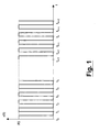
- Figure 1 shows a graph of a periodic signal x(t) with amplitude P0 and frequency fx.
- each period of the periodic signal x(t) starts with a rising edge.
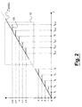
- the normalised phase ⁇ x(t)/2 ⁇ of the signal x(t) is equal to an integer value, as shown in Figure 2 .
- a counter is firstly provided.
- the counter value is increased upon each occurrence of an event marking the evolution of the data signal.
- Figure 2 shows for example a counter c(t) which is increased at each rising edge of the periodic signal x(t).
- the counter c(t) is equal to the normalised phase ⁇ x(t)/2 ⁇ with a phase error ⁇ (t).
- x(t) is a periodic signal.
- the method of measurement according to the present invention can be applied to data signals, i.e. to signals which comprise a sequence of bit with bit-rate fx.
- each bit “1” or “0” must be encoded so that in each period there occurs an event for incrementing the counter c(t). It is the case, for example, of bipolar encodings, wherein the bit "1” is encoded as a "high-low” transition and the bit "0” is encoded as a "low-high” transition. Therefore, independently of the bit sequence, each period includes a transition; the counter c(t) is then increased each time a transition occurs.
- fs sampling frequency
- the counter c(t) is the normalised phase ⁇ x(t)/2 ⁇ affected by an error ⁇ (t).
- the sampling frequency fs is such that the sampling instants always occur in the same position relatively to the signal periods, the phase error affecting each sample of the sequence ⁇ s n ⁇ is the same for all the samples.
- the sampling frequency fs is equal to fx or to an integer sub-multiple of the frequency fx, the sequence ⁇ s n ⁇ allows to recover the normalised phase ⁇ x(t)/2 ⁇ , shifted by a phase offset.
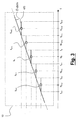
- Figure 3 shows an ideal case, in which fs is exactly equal to fx. It can be noticed that all the sampling instants are placed in the middle of each period; therefore, the sample sequence ⁇ s n ⁇ is a ramp, which is analogous to the normalised phase ⁇ x(t)/2 ⁇ ramp, shifted by a constant phase offset.
- fs is not exactly equal to fx (or to an integer sub-multiple of fx).
- the frequency fs is derived from the reference timing signal, thus being a sub-multiple of one of the synchronous hierarchy frequencies.
- the signal x(t) may be either a synchronous signal, or an asynchronous signal.
- the detuning between fs and fx may be of a few parts per million; in the second case, the detuning between fs and fx may be of a few percentage points.
- Figures 4a and 4b show the effect of sampling in two real cases, wherein the sampling frequency fs and the frequency fx are detuned.
- Figure 4a refers to the case wherein fs is higher than fx. It is assumed that in a certain signal period, for example the period comprised between t n-3 e t n-2 , the sampling instant ts n-2 is placed in the middle of the period. As fs is higher than fx, in the following signal periods the sampling instants will tend to move towards the beginning of the period. Therefore, each sample of the sequence ⁇ S n ⁇ is affected by a phase error, with respect to the normalised phase ⁇ x(t)/2 ⁇ , that changes for each sample.
- sampling period 1/fs is lower than the signal period, after a certain number of sampling instants there will be a signal period (between t n e t n+1 in Figure 4a ) comprising two sampling instants (ts n+1 e ts n+2 ).
- the resulting sample sequence ⁇ s n ⁇ thus exhibits an anomaly with respect to the linear trend of the normalised phase ramp.
- Figure 4b shows the case wherein fs is lower than fx.
- the sampling instant in a certain signal period, for instance the one included between t n-3 e t n-2 , the sampling instant is placed exactly in the middle of the signal period.
- the following sampling instants tend to move toward the end of the signal period.
- each sample of the sequence ⁇ S n ⁇ is affected by a different phase error.
- the sampling period 1/fs is higher than the signal period, after a certain number of sampling instants there will be a signal period (between t n e t n+1 in Figure 4b ) comprising no sampling instants.
- the resulting sample sequence ⁇ S n ⁇ thus exhibits an anomaly with respect to the linear trend of the normalised phase ramp.
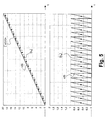
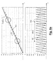
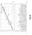
- Figures 5 , 6a and 6b show the effect of the detuning between fs and fx over the phase error occurring when considering at each sampling instant ts n the sample s n instead of the actual value of normalised phase ⁇ x(ts n )/2 ⁇ , according to the known method.
- Figure 5 is referred to the ideal case wherein fs is equal to fx.
- Figures 6a and 6b are referred to two real cases wherein fs is respectively higher and lower than fx.
- Figure 6a shows a real case in which fs is higher than fx.
- the sample sequence ⁇ s n ⁇ exhibits anomalies, as described by reference to Figure 4a .
- Such anomalies are periodic with a period WTJ.
- the sequence of phase errors ⁇ n ⁇ has a saw-tooth shape with period WTJ. Filtering such a phase error thus requires filtering a 1/WTJ frequency component.
- Figure 6b shows a second real case in which fs is lower than fx.
- the sample sequence ⁇ s n ⁇ exhibits anomalies, as described by reference to Figure 4b .
- Such anomalies are periodic with a period WTJ.
- the sequence of phase errors ⁇ n ⁇ has a saw-tooth shape with period WTJ. Filtering such a phase error thus requires filtering a 1/WTJ frequency component.
- N 1 / fx / ⁇ ⁇ T .
- sampling frequency fs it is not possible to modify the sampling frequency fs, as it is derived by the synchronous hierarchy frequencies by means of dividers, which provides integer sub-multiples of fs. Using a sub-multiple of fs, however, does not eliminate anomalies of the sequence ⁇ s n ⁇ and the consequent periodicity of the sequence of phase errors ⁇ n ⁇ .
- a method for digitally measuring the phase of a signal wherein the spectral distribution of the phase error can be modified.
- the method according to the invention comprise an additional step with respect to the known method, wherein the counter c(t) is sampled at a first sampling frequency fc uncorrelated from the signal frequency fx, thus obtaining a first sample sequence ⁇ c n ⁇ .
- Said first sample sequence ⁇ c n ⁇ is in turn sampled at a second sampling frequency fs, thus obtaining a second sample sequence ⁇ s n ⁇ , which is finally digitally processed.
- the second sequence ⁇ S n ⁇ exhibits anomalies with respect to the ramp of the normalised phase with a period WTJ mainly dependent on the ratio between the first sampling frequency fc and the signal frequency fx.
- WTJ the ratio between the first sampling frequency fc and the signal frequency fx.
- phase error ⁇ (t) phase error ⁇ (t).
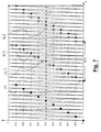
- Figure 7 a graph of the error as a function of time ⁇ (t) is reported.
- the sequence ( ⁇ n' ), represented by triangles in Figure 7 is the sequence of phase errors affecting the sequence ⁇ s n ⁇ in the ideal case, wherein fs is equal to fx.
- each phase error ⁇ n' affecting each sample s n is constant, the sequence ⁇ s n ⁇ thus corresponding to the normalised phase shifted by an offset.
- the sequence ⁇ n" ⁇ represented in Figure 7 by circles, is the sequence of phase errors affecting the sequence ⁇ s n ⁇ in a real case, wherein fs and fx are detuned.
- the phase error ⁇ n" affecting each sample s n is not constant, and the sequence ⁇ n" ⁇ has period WTJ.
- the sequence ⁇ n"' ⁇ is the sequence of phase errors affecting the sequence ⁇ s n ⁇ in an embodiment of the method according to the present invention.
- the sequence ⁇ n"' ⁇ is not periodic, since the sampling time instants always fall in different positions of the signal period.
- the formulas describing ⁇ n"' ) will be derived.
- n K ⁇ ⁇ ⁇ mn m + 1 + Km m + 1 ⁇ m + 1 m ⁇ n ⁇ .
- the sequence of phase errors when filtered, is substantially independent from K, i.e. from d; in other words, the sequence of phase errors is independent from the detuning between fs and fx.
- the first two terms of the summation are always integer numbers, while the third term provides a fractional number.
- the third term is an integer number only when multiplied by a number higher than m, i.e. the two following conditions must be satisfied:
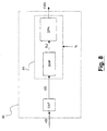
- FIG. 8 shows a known device for digitally measuring the phase of a signal.
- the device 80 comprises a counter block CNT, with an input port for receiving a signal, and an output port connected to the input port of a digital device 81, in turn comprising a sampler SMP connected to a processor DPA, which implements a digital processing algorithm.
- a signal x(t) at the input of the device 80 is received from the counter CNT, which outputs a counter c(t).
- Said counter c(t) is sent to the digital device 81, which is synchronised by a timing signal with frequency fs.
- FIG 9 shows a device for digitally measuring the phase of a signal according to the present invention.
- Said device is advantageously employed into a network element of a synchronous transmission network.
- the device 90 comprises a counter block CNT, with an input port for receiving a signal and an output port connected to an input port of a register RG.
- the register RG has an output port which is connected to an input of a digital device 91, in turn comprising a sampler SMP connected to a processor DPA, which implements a digital processing algorithm.
- a signal x(t) at the input of the device 90 is received by the counter block CNT, which extrapolates a counter c(t) from the signal x(t).
- Said counter c(t) is sent to the register RG, which samples it at a first sampling frequency fc, thus obtaining a first sample sequence ⁇ C n ⁇ .
- Said first sample sequence ⁇ C n ⁇ is sent to the digital device 91, which is synchronised by a timing signal with frequency fs.
- the sequence ⁇ C n ⁇ is firstly sampled by the sampler SMP with the sampling frequency fs, thus obtaining a sample sequence ⁇ S n ⁇ .
- the sampler then sends the sample sequence ⁇ S n ⁇ to the processor DPA, which digitally processes the sequence and possibly estimates the frequency of the input signal x(t).
- Such a device can be employed, for example, in network nodes of a synchronous network, as mentioned before.
- the frequency fs is obtained by a frequency of the synchronous hierarchy by suitable dividers, fs thus being an integer sub-multiple of a frequency of the synchronous hierarchy.
- fc is generated by a local oscillator uncorrelated from the timing signal available in the network element. This guarantees the uncorrelation between fc and fx.
- the device for digitally measuring the phase according to the invention can be employed into a device for the regeneration of a periodic signal x(t), and, more in particular, into devices such as the so-called “Phase Locked Loop” (PLL).
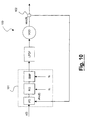
- Figure 10 shows a PLL 100 wherein the phase recovery is performed according to the method of the present invention.
- the PLL 100 comprises a phase device for phase digital measurement 101, a low-pass digital filter LPDF and a voltage-controlled local oscillator VCO.
- a junction 102 with two branches is provided, wherein a first branch is the output port of the PLL, while the second branch is connected to the device for phase digital measurement 101.
- the device for phase digital measurement 101 in turn comprises a phase detector PD, a register RG operating at a first sampling frequency fc and a sampler SMP working at a second sampling frequency fs.
Landscapes
- Engineering & Computer Science (AREA)
- Computer Networks & Wireless Communication (AREA)
- Signal Processing (AREA)
- Physics & Mathematics (AREA)
- General Physics & Mathematics (AREA)
- Synchronisation In Digital Transmission Systems (AREA)
- Measuring Phase Differences (AREA)
- Stabilization Of Oscillater, Synchronisation, Frequency Synthesizers (AREA)
Claims (10)
- Procédé de mesure numérique de la phase (Γx(t)) d'un signal de données (x(t)) ayant une fréquence fx se déplaçant dans un réseau de transmission, ledit procédé comprenant les étapes suivantes :- fourniture d'un compteur (c(t)) ;- augmentation d'une valeur dudit compteur (c(t)) suite à chaque occurrence d'un événement marquant l'évolution du signal de données (x(t)) ayant la fréquence fx ;- échantillonnage du compteur (c(t)) à une première fréquence d'échantillonnage fc non corrélée à ladite fréquence fx, pour obtenir une première séquence d'échantillon ({cn}),- échantillonnage de ladite première séquence d'échantillon ({cn) à une seconde fréquence d'échantillonnage fs, pour obtenir une seconde séquence d'échantillon ({sn}) ; et- traitement numérique de ladite seconde séquence d'échantillon ({sn}) afin d'estimer ladite phase (Γx(t)) dudit signal de données (x(t)),ledit procédé étant caractérisé en ce que ladite étape d'échantillonnage dudit compteur (c(t)) à ladite première fréquence d'échantillonnage fc non corrélée à ladite fréquence fx est réalisée en échantillonnant ledit compteur (c(t)) à ladite fréquence fc avec fc=α, où α est un nombre irrationnel.
- Procédé selon la revendication 1, dans lequel l'étape de traitement numérique de ladite seconde séquence d'échantillon ({sn}) comprend le filtrage numérique de ladite seconde séquence d'échantillon ({sn}).
- Procédé selon l'une quelconque des revendications précédentes, dans lequel ladite fréquence fx dudit signal de données (x(t)) et ladite seconde fréquence d'échantillonnage fs sont des fréquences d'un système de transmission synchrone.
- Procédé selon l'une quelconque des revendications précédentes, dans lequel ladite première fréquence d'échantillonnage fc est générée par un oscillateur local indépendant de ladite fréquence fx et de ladite seconde fréquence d'échantillonnage fs.
- Dispositif de mesure numérique de la phase (rx(t)) d'un signal de données (x(t)) ayant une fréquence fx se déplaçant dans un réseau de transmission, ledit dispositif comprenant :- un bloc compteur (CNT), ledit bloc compteur (CNT) augmentant une valeur d'un compteur (c(t)) suite à chaque occurrence d'un événement marquant l'évolution du signal de données (x(t)) ayant la fréquence fx ; et- un registre (RG), ledit registre (RG) échantillonnant le compteur (c(t)) à une première fréquence d'échantillonnage fc non corrélée à ladite fréquence fx, pour obtenir une première séquence d'échantillon ({cn}),- un échantillonneur (SMP), ledit échantillonneur (SMP) échantillonnant ladite première séquence d'échantillon ({cn}) à une seconde fréquence d'échantillonnage fs, pour obtenir une seconde séquence d'échantillon ({Sn}) : et- un processeur (DPA), ledit processeur (DPA) effectuant un traitement numérique de ladite seconde séquence d'échantillon ({sn}) afin d'estimer ladite phase (Γx(t)) dudit signal de données (x(t)),ledit dispositif étant caractérisé en ce que ledit registre (RG) est un registre échantillonnant le compteur (c(t)) à une première fréquence d'échantillonnage fc avec fc=α fx, où α est un nombre irrationnel.
- Dispositif selon la revendication 5, dans lequel ledit processeur (DPA) effectue un traitement numérique sur ladite seconde séquence d'échantillon ({sn}) en filtrant numériquement ladite seconde séquence d'échantillon ({sn}).
- Dispositif selon l'une quelconque des revendications 5-6, dans lequel ladite fréquence fx dudit signal de données (x(t)) et ladite seconde fréquence d'échantillonnage fs sont des fréquences d'un système de transmission synchrone.
- Dispositif selon l'une quelconque des revendications 5- 7, dans lequel ladite première fréquence d'échantillonnage fc est générée par un oscillateur local indépendant de ladite fréquence fx et de ladite seconde fréquence d'échantillonnage fs.
- Dispositif selon l'une quelconque des revendications 5 à 8, dans lequel ledit dispositif fait partie d'une boucle à verrouillage de phase (100).
- Élément de réseau comprenant un dispositif selon l'une quelconque des revendications 5 à 9.
Priority Applications (5)
| Application Number | Priority Date | Filing Date | Title |
|---|---|---|---|
| AT04292278T ATE507483T1 (de) | 2004-09-22 | 2004-09-22 | Verfahren und vorrichtung zur digitalen phasenmessung eines signals |
| DE602004032438T DE602004032438D1 (de) | 2004-09-22 | 2004-09-22 | Verfahren und Vorrichtung zur digitalen Phasenmessung eines Signals |
| EP04292278A EP1640733B1 (fr) | 2004-09-22 | 2004-09-22 | Procédé et dispositif pour la mesure de la phase d'un signal |
| US11/192,357 US20060061393A1 (en) | 2004-09-22 | 2005-07-29 | Method and device for digitally measuring the phase of a signal |
| CN200510103568.7A CN1753311A (zh) | 2004-09-22 | 2005-09-21 | 用于数字地测量信号的相位的方法和设备 |
Applications Claiming Priority (1)
| Application Number | Priority Date | Filing Date | Title |
|---|---|---|---|
| EP04292278A EP1640733B1 (fr) | 2004-09-22 | 2004-09-22 | Procédé et dispositif pour la mesure de la phase d'un signal |
Publications (2)
| Publication Number | Publication Date |
|---|---|
| EP1640733A1 EP1640733A1 (fr) | 2006-03-29 |
| EP1640733B1 true EP1640733B1 (fr) | 2011-04-27 |
Family
ID=34931406
Family Applications (1)
| Application Number | Title | Priority Date | Filing Date |
|---|---|---|---|
| EP04292278A Expired - Lifetime EP1640733B1 (fr) | 2004-09-22 | 2004-09-22 | Procédé et dispositif pour la mesure de la phase d'un signal |
Country Status (5)
| Country | Link |
|---|---|
| US (1) | US20060061393A1 (fr) |
| EP (1) | EP1640733B1 (fr) |
| CN (1) | CN1753311A (fr) |
| AT (1) | ATE507483T1 (fr) |
| DE (1) | DE602004032438D1 (fr) |
Families Citing this family (2)
| Publication number | Priority date | Publication date | Assignee | Title |
|---|---|---|---|---|
| EP2282229A1 (fr) * | 2009-08-07 | 2011-02-09 | CCS Technology, Inc. | Dispositif optique avec des connectuers et procédé pour la connexion d'unités récepteur-émetteur par un tel dispositif |
| US8890507B2 (en) * | 2010-05-19 | 2014-11-18 | Tektronix, Inc. | Phase transient response measurements using automatic frequency estimation |
Family Cites Families (5)
| Publication number | Priority date | Publication date | Assignee | Title |
|---|---|---|---|---|
| US5084669A (en) * | 1990-03-08 | 1992-01-28 | Telefonaktiebolaget L M Ericsson | Direct phase digitization |
| US5373255A (en) * | 1993-07-28 | 1994-12-13 | Motorola, Inc. | Low-power, jitter-compensated phase locked loop and method therefor |
| DE4336240A1 (de) * | 1993-10-23 | 1995-04-27 | Sel Alcatel Ag | Schaltungsanordnung für einen digitalen Phasenkomparator |
| US6266799B1 (en) * | 1997-10-02 | 2001-07-24 | Xaqti, Corporation | Multi-phase data/clock recovery circuitry and methods for implementing same |
| US6246738B1 (en) * | 1998-11-19 | 2001-06-12 | Pmc-Sierra Ltd. | Phase modulated reduction of clock wander in synchronous wide area networks |
-
2004
- 2004-09-22 EP EP04292278A patent/EP1640733B1/fr not_active Expired - Lifetime
- 2004-09-22 DE DE602004032438T patent/DE602004032438D1/de not_active Expired - Lifetime
- 2004-09-22 AT AT04292278T patent/ATE507483T1/de not_active IP Right Cessation
-
2005
- 2005-07-29 US US11/192,357 patent/US20060061393A1/en not_active Abandoned
- 2005-09-21 CN CN200510103568.7A patent/CN1753311A/zh active Pending
Also Published As
| Publication number | Publication date |
|---|---|
| EP1640733A1 (fr) | 2006-03-29 |
| ATE507483T1 (de) | 2011-05-15 |
| DE602004032438D1 (de) | 2011-06-09 |
| US20060061393A1 (en) | 2006-03-23 |
| CN1753311A (zh) | 2006-03-29 |
Similar Documents
| Publication | Publication Date | Title |
|---|---|---|
| US7272201B2 (en) | System for synchronous sampling and time-of-day clocking using an encoded time signal | |
| EP0849907B1 (fr) | Dispositif et procédé pour la mesure de phases | |
| EP1178609B1 (fr) | Détecteur de phase | |
| US6326851B1 (en) | Digital phase-domain PLL frequency synthesizer | |
| KR100547831B1 (ko) | 가변 데이터 전송률에 대응이 가능한 클럭 및 데이터 복원장치 | |
| CA2253461C (fr) | Boucle fermee a frequence d'entree multiple | |
| US5757652A (en) | Electrical signal jitter and wander measurement system and method | |
| EP3301835A1 (fr) | Appareil et procédés de mappage d'horloge asynchrone | |
| US20090003504A1 (en) | Method for frequency compensation in timing recovery | |
| US8358939B2 (en) | Optical communication device | |
| KR101054638B1 (ko) | 데이터 재생 회로 | |
| JP5002528B2 (ja) | ディジタル位相検出器およびpll | |
| US6246738B1 (en) | Phase modulated reduction of clock wander in synchronous wide area networks | |
| US9444615B2 (en) | Low latency digital jitter termination for repeater circuits | |
| KR100862671B1 (ko) | 복수 개의 출력신호들의 발생을 위한 위상동기루프 | |
| CN103983296A (zh) | 用于检测测量值的方法 | |
| EP1640733B1 (fr) | Procédé et dispositif pour la mesure de la phase d'un signal | |
| KR20140135113A (ko) | 클록 및 데이터 복원 회로에서 수신된 데이터 신호를 추적하는 시스템 및 방법 | |
| CN113839670A (zh) | 一种高性能频率改正方法、频率改正系统和改进的锁相环 | |
| EP4102765A1 (fr) | Dispositif de synchronisation temporelle, système de synchronisation temporelle et procédé de synchronisation temporelle | |
| CN106067811A (zh) | 一种应用于亚速率时钟数据恢复电路的Bang‑Bang鉴相器 | |
| WO2004006478A1 (fr) | Systeme et procede de recuperation temporelle de reseau | |
| Gautam et al. | Double demodulation type open-loop synchronization method for single-phase system | |
| Stavrinides et al. | Desynchronization crisis induced intermittency in a master–slave PLL configuration | |
| Bonello et al. | Preliminary experimental results for the development of the new Italian synchronization network |
Legal Events
| Date | Code | Title | Description |
|---|---|---|---|
| PUAI | Public reference made under article 153(3) epc to a published international application that has entered the european phase |
Free format text: ORIGINAL CODE: 0009012 |
|
| AK | Designated contracting states |
Kind code of ref document: A1 Designated state(s): AT BE BG CH CY CZ DE DK EE ES FI FR GB GR HU IE IT LI LU MC NL PL PT RO SE SI SK TR |
|
| AX | Request for extension of the european patent |
Extension state: AL HR LT LV MK |
|
| 17P | Request for examination filed |
Effective date: 20060928 |
|
| RIN1 | Information on inventor provided before grant (corrected) |
Inventor name: RAZZETTI, LUCA Inventor name: GASTALDELLO, STEFANO Inventor name: SKERLJ, MAURIZIO |
|
| 17Q | First examination report despatched |
Effective date: 20061026 |
|
| AKX | Designation fees paid |
Designated state(s): AT BE BG CH CY CZ DE DK EE ES FI FR GB GR HU IE IT LI LU MC NL PL PT RO SE SI SK TR |
|
| RAP1 | Party data changed (applicant data changed or rights of an application transferred) |
Owner name: ALCATEL LUCENT |
|
| GRAP | Despatch of communication of intention to grant a patent |
Free format text: ORIGINAL CODE: EPIDOSNIGR1 |
|
| GRAS | Grant fee paid |
Free format text: ORIGINAL CODE: EPIDOSNIGR3 |
|
| GRAA | (expected) grant |
Free format text: ORIGINAL CODE: 0009210 |
|
| AK | Designated contracting states |
Kind code of ref document: B1 Designated state(s): AT BE BG CH CY CZ DE DK EE ES FI FR GB GR HU IE IT LI LU MC NL PL PT RO SE SI SK TR |
|
| REG | Reference to a national code |
Ref country code: GB Ref legal event code: FG4D |
|
| REG | Reference to a national code |
Ref country code: CH Ref legal event code: EP |
|
| REG | Reference to a national code |
Ref country code: IE Ref legal event code: FG4D |
|
| REF | Corresponds to: |
Ref document number: 602004032438 Country of ref document: DE Date of ref document: 20110609 Kind code of ref document: P |
|
| REG | Reference to a national code |
Ref country code: DE Ref legal event code: R096 Ref document number: 602004032438 Country of ref document: DE Effective date: 20110609 |
|
| REG | Reference to a national code |
Ref country code: NL Ref legal event code: VDEP Effective date: 20110427 |
|
| PG25 | Lapsed in a contracting state [announced via postgrant information from national office to epo] |
Ref country code: SE Free format text: LAPSE BECAUSE OF FAILURE TO SUBMIT A TRANSLATION OF THE DESCRIPTION OR TO PAY THE FEE WITHIN THE PRESCRIBED TIME-LIMIT Effective date: 20110427 Ref country code: PT Free format text: LAPSE BECAUSE OF FAILURE TO SUBMIT A TRANSLATION OF THE DESCRIPTION OR TO PAY THE FEE WITHIN THE PRESCRIBED TIME-LIMIT Effective date: 20110829 |
|
| PG25 | Lapsed in a contracting state [announced via postgrant information from national office to epo] |
Ref country code: SI Free format text: LAPSE BECAUSE OF FAILURE TO SUBMIT A TRANSLATION OF THE DESCRIPTION OR TO PAY THE FEE WITHIN THE PRESCRIBED TIME-LIMIT Effective date: 20110427 Ref country code: CY Free format text: LAPSE BECAUSE OF FAILURE TO SUBMIT A TRANSLATION OF THE DESCRIPTION OR TO PAY THE FEE WITHIN THE PRESCRIBED TIME-LIMIT Effective date: 20110427 Ref country code: FI Free format text: LAPSE BECAUSE OF FAILURE TO SUBMIT A TRANSLATION OF THE DESCRIPTION OR TO PAY THE FEE WITHIN THE PRESCRIBED TIME-LIMIT Effective date: 20110427 Ref country code: ES Free format text: LAPSE BECAUSE OF FAILURE TO SUBMIT A TRANSLATION OF THE DESCRIPTION OR TO PAY THE FEE WITHIN THE PRESCRIBED TIME-LIMIT Effective date: 20110807 Ref country code: BE Free format text: LAPSE BECAUSE OF FAILURE TO SUBMIT A TRANSLATION OF THE DESCRIPTION OR TO PAY THE FEE WITHIN THE PRESCRIBED TIME-LIMIT Effective date: 20110427 Ref country code: GR Free format text: LAPSE BECAUSE OF FAILURE TO SUBMIT A TRANSLATION OF THE DESCRIPTION OR TO PAY THE FEE WITHIN THE PRESCRIBED TIME-LIMIT Effective date: 20110728 Ref country code: AT Free format text: LAPSE BECAUSE OF FAILURE TO SUBMIT A TRANSLATION OF THE DESCRIPTION OR TO PAY THE FEE WITHIN THE PRESCRIBED TIME-LIMIT Effective date: 20110427 |
|
| PG25 | Lapsed in a contracting state [announced via postgrant information from national office to epo] |
Ref country code: NL Free format text: LAPSE BECAUSE OF FAILURE TO SUBMIT A TRANSLATION OF THE DESCRIPTION OR TO PAY THE FEE WITHIN THE PRESCRIBED TIME-LIMIT Effective date: 20110427 |
|
| PG25 | Lapsed in a contracting state [announced via postgrant information from national office to epo] |
Ref country code: CZ Free format text: LAPSE BECAUSE OF FAILURE TO SUBMIT A TRANSLATION OF THE DESCRIPTION OR TO PAY THE FEE WITHIN THE PRESCRIBED TIME-LIMIT Effective date: 20110427 Ref country code: EE Free format text: LAPSE BECAUSE OF FAILURE TO SUBMIT A TRANSLATION OF THE DESCRIPTION OR TO PAY THE FEE WITHIN THE PRESCRIBED TIME-LIMIT Effective date: 20110427 |
|
| RAP2 | Party data changed (patent owner data changed or rights of a patent transferred) |
Owner name: ALCATEL LUCENT |
|
| PG25 | Lapsed in a contracting state [announced via postgrant information from national office to epo] |
Ref country code: SK Free format text: LAPSE BECAUSE OF FAILURE TO SUBMIT A TRANSLATION OF THE DESCRIPTION OR TO PAY THE FEE WITHIN THE PRESCRIBED TIME-LIMIT Effective date: 20110427 Ref country code: PL Free format text: LAPSE BECAUSE OF FAILURE TO SUBMIT A TRANSLATION OF THE DESCRIPTION OR TO PAY THE FEE WITHIN THE PRESCRIBED TIME-LIMIT Effective date: 20110427 Ref country code: DK Free format text: LAPSE BECAUSE OF FAILURE TO SUBMIT A TRANSLATION OF THE DESCRIPTION OR TO PAY THE FEE WITHIN THE PRESCRIBED TIME-LIMIT Effective date: 20110427 Ref country code: RO Free format text: LAPSE BECAUSE OF FAILURE TO SUBMIT A TRANSLATION OF THE DESCRIPTION OR TO PAY THE FEE WITHIN THE PRESCRIBED TIME-LIMIT Effective date: 20110427 |
|
| REG | Reference to a national code |
Ref country code: CH Ref legal event code: PCOW Free format text: ALCATEL LUCENT;3, AVENUE OCTAVE GREARD;75007 PARIS (FR) |
|
| PLBE | No opposition filed within time limit |
Free format text: ORIGINAL CODE: 0009261 |
|
| STAA | Information on the status of an ep patent application or granted ep patent |
Free format text: STATUS: NO OPPOSITION FILED WITHIN TIME LIMIT |
|
| 26N | No opposition filed |
Effective date: 20120130 |
|
| PG25 | Lapsed in a contracting state [announced via postgrant information from national office to epo] |
Ref country code: MC Free format text: LAPSE BECAUSE OF NON-PAYMENT OF DUE FEES Effective date: 20110930 |
|
| REG | Reference to a national code |
Ref country code: CH Ref legal event code: PL |
|
| REG | Reference to a national code |
Ref country code: DE Ref legal event code: R097 Ref document number: 602004032438 Country of ref document: DE Effective date: 20120130 |
|
| PG25 | Lapsed in a contracting state [announced via postgrant information from national office to epo] |
Ref country code: IT Free format text: LAPSE BECAUSE OF FAILURE TO SUBMIT A TRANSLATION OF THE DESCRIPTION OR TO PAY THE FEE WITHIN THE PRESCRIBED TIME-LIMIT Effective date: 20110427 |
|
| REG | Reference to a national code |
Ref country code: IE Ref legal event code: MM4A |
|
| PG25 | Lapsed in a contracting state [announced via postgrant information from national office to epo] |
Ref country code: IE Free format text: LAPSE BECAUSE OF NON-PAYMENT OF DUE FEES Effective date: 20110922 Ref country code: CH Free format text: LAPSE BECAUSE OF NON-PAYMENT OF DUE FEES Effective date: 20110930 Ref country code: LI Free format text: LAPSE BECAUSE OF NON-PAYMENT OF DUE FEES Effective date: 20110930 |
|
| PG25 | Lapsed in a contracting state [announced via postgrant information from national office to epo] |
Ref country code: LU Free format text: LAPSE BECAUSE OF NON-PAYMENT OF DUE FEES Effective date: 20110922 |
|
| PG25 | Lapsed in a contracting state [announced via postgrant information from national office to epo] |
Ref country code: BG Free format text: LAPSE BECAUSE OF FAILURE TO SUBMIT A TRANSLATION OF THE DESCRIPTION OR TO PAY THE FEE WITHIN THE PRESCRIBED TIME-LIMIT Effective date: 20110727 |
|
| PG25 | Lapsed in a contracting state [announced via postgrant information from national office to epo] |
Ref country code: TR Free format text: LAPSE BECAUSE OF FAILURE TO SUBMIT A TRANSLATION OF THE DESCRIPTION OR TO PAY THE FEE WITHIN THE PRESCRIBED TIME-LIMIT Effective date: 20110427 |
|
| PG25 | Lapsed in a contracting state [announced via postgrant information from national office to epo] |
Ref country code: HU Free format text: LAPSE BECAUSE OF FAILURE TO SUBMIT A TRANSLATION OF THE DESCRIPTION OR TO PAY THE FEE WITHIN THE PRESCRIBED TIME-LIMIT Effective date: 20110427 |
|
| REG | Reference to a national code |
Ref country code: FR Ref legal event code: GC Effective date: 20131018 |
|
| REG | Reference to a national code |
Ref country code: FR Ref legal event code: RG Effective date: 20141016 |
|
| REG | Reference to a national code |
Ref country code: FR Ref legal event code: PLFP Year of fee payment: 12 |
|
| PGFP | Annual fee paid to national office [announced via postgrant information from national office to epo] |
Ref country code: GB Payment date: 20150917 Year of fee payment: 12 Ref country code: DE Payment date: 20150922 Year of fee payment: 12 |
|
| PGFP | Annual fee paid to national office [announced via postgrant information from national office to epo] |
Ref country code: FR Payment date: 20150922 Year of fee payment: 12 |
|
| REG | Reference to a national code |
Ref country code: DE Ref legal event code: R119 Ref document number: 602004032438 Country of ref document: DE |
|
| GBPC | Gb: european patent ceased through non-payment of renewal fee |
Effective date: 20160922 |
|
| REG | Reference to a national code |
Ref country code: FR Ref legal event code: ST Effective date: 20170531 |
|
| PG25 | Lapsed in a contracting state [announced via postgrant information from national office to epo] |
Ref country code: GB Free format text: LAPSE BECAUSE OF NON-PAYMENT OF DUE FEES Effective date: 20160922 Ref country code: DE Free format text: LAPSE BECAUSE OF NON-PAYMENT OF DUE FEES Effective date: 20170401 Ref country code: FR Free format text: LAPSE BECAUSE OF NON-PAYMENT OF DUE FEES Effective date: 20160930 |