EP1643641A2 - Hochfrequenz-Heizvorrichtung, Halbleiterfabrikationsvorrichtung, und Lichtquellevorrichtung - Google Patents
Hochfrequenz-Heizvorrichtung, Halbleiterfabrikationsvorrichtung, und Lichtquellevorrichtung Download PDFInfo
- Publication number
- EP1643641A2 EP1643641A2 EP05021264A EP05021264A EP1643641A2 EP 1643641 A2 EP1643641 A2 EP 1643641A2 EP 05021264 A EP05021264 A EP 05021264A EP 05021264 A EP05021264 A EP 05021264A EP 1643641 A2 EP1643641 A2 EP 1643641A2
- Authority
- EP
- European Patent Office
- Prior art keywords
- microwave
- antenna
- reflected wave
- oscillator
- amplifier
- Prior art date
- Legal status (The legal status is an assumption and is not a legal conclusion. Google has not performed a legal analysis and makes no representation as to the accuracy of the status listed.)
- Withdrawn
Links
Images





Classifications
-
- H—ELECTRICITY
- H03—ELECTRONIC CIRCUITRY
- H03B—GENERATION OF OSCILLATIONS, DIRECTLY OR BY FREQUENCY-CHANGING, BY CIRCUITS EMPLOYING ACTIVE ELEMENTS WHICH OPERATE IN A NON-SWITCHING MANNER; GENERATION OF NOISE BY SUCH CIRCUITS
- H03B5/00—Generation of oscillations using amplifier with regenerative feedback from output to input
- H03B5/30—Generation of oscillations using amplifier with regenerative feedback from output to input with frequency-determining element being electromechanical resonator
- H03B5/32—Generation of oscillations using amplifier with regenerative feedback from output to input with frequency-determining element being electromechanical resonator being a piezoelectric resonator
- H03B5/326—Generation of oscillations using amplifier with regenerative feedback from output to input with frequency-determining element being electromechanical resonator being a piezoelectric resonator the resonator being an acoustic wave device, e.g. SAW or BAW device
-
- H—ELECTRICITY
- H10—SEMICONDUCTOR DEVICES; ELECTRIC SOLID-STATE DEVICES NOT OTHERWISE PROVIDED FOR
- H10P—GENERIC PROCESSES OR APPARATUS FOR THE MANUFACTURE OR TREATMENT OF DEVICES COVERED BY CLASS H10
- H10P95/00—Generic processes or apparatus for manufacture or treatments not covered by the other groups of this subclass
-
- H—ELECTRICITY
- H01—ELECTRIC ELEMENTS
- H01J—ELECTRIC DISCHARGE TUBES OR DISCHARGE LAMPS
- H01J37/00—Discharge tubes with provision for introducing objects or material to be exposed to the discharge, e.g. for the purpose of examination or processing thereof
- H01J37/32—Gas-filled discharge tubes
- H01J37/32009—Arrangements for generation of plasma specially adapted for examination or treatment of objects, e.g. plasma sources
- H01J37/32192—Microwave generated discharge
-
- H—ELECTRICITY
- H01—ELECTRIC ELEMENTS
- H01J—ELECTRIC DISCHARGE TUBES OR DISCHARGE LAMPS
- H01J37/00—Discharge tubes with provision for introducing objects or material to be exposed to the discharge, e.g. for the purpose of examination or processing thereof
- H01J37/32—Gas-filled discharge tubes
- H01J37/32009—Arrangements for generation of plasma specially adapted for examination or treatment of objects, e.g. plasma sources
- H01J37/32192—Microwave generated discharge
- H01J37/32201—Generating means
-
- H—ELECTRICITY
- H01—ELECTRIC ELEMENTS
- H01J—ELECTRIC DISCHARGE TUBES OR DISCHARGE LAMPS
- H01J37/00—Discharge tubes with provision for introducing objects or material to be exposed to the discharge, e.g. for the purpose of examination or processing thereof
- H01J37/32—Gas-filled discharge tubes
- H01J37/32009—Arrangements for generation of plasma specially adapted for examination or treatment of objects, e.g. plasma sources
- H01J37/32192—Microwave generated discharge
- H01J37/32266—Means for controlling power transmitted to the plasma
-
- H—ELECTRICITY
- H01—ELECTRIC ELEMENTS
- H01J—ELECTRIC DISCHARGE TUBES OR DISCHARGE LAMPS
- H01J37/00—Discharge tubes with provision for introducing objects or material to be exposed to the discharge, e.g. for the purpose of examination or processing thereof
- H01J37/32—Gas-filled discharge tubes
- H01J37/32009—Arrangements for generation of plasma specially adapted for examination or treatment of objects, e.g. plasma sources
- H01J37/32192—Microwave generated discharge
- H01J37/32302—Plural frequencies
-
- H—ELECTRICITY
- H01—ELECTRIC ELEMENTS
- H01J—ELECTRIC DISCHARGE TUBES OR DISCHARGE LAMPS
- H01J37/00—Discharge tubes with provision for introducing objects or material to be exposed to the discharge, e.g. for the purpose of examination or processing thereof
- H01J37/32—Gas-filled discharge tubes
- H01J37/32009—Arrangements for generation of plasma specially adapted for examination or treatment of objects, e.g. plasma sources
- H01J37/32192—Microwave generated discharge
- H01J37/32311—Circuits specially adapted for controlling the microwave discharge
-
- H—ELECTRICITY
- H03—ELECTRONIC CIRCUITRY
- H03H—IMPEDANCE NETWORKS, e.g. RESONANT CIRCUITS; RESONATORS
- H03H7/00—Multiple-port networks comprising only passive electrical elements as network components
- H03H7/18—Networks for phase shifting
-
- H—ELECTRICITY
- H05—ELECTRIC TECHNIQUES NOT OTHERWISE PROVIDED FOR
- H05B—ELECTRIC HEATING; ELECTRIC LIGHT SOURCES NOT OTHERWISE PROVIDED FOR; CIRCUIT ARRANGEMENTS FOR ELECTRIC LIGHT SOURCES, IN GENERAL
- H05B6/00—Heating by electric, magnetic or electromagnetic fields
- H05B6/64—Heating using microwaves
- H05B6/66—Circuits
- H05B6/68—Circuits for monitoring or control
- H05B6/686—Circuits comprising a signal generator and power amplifier, e.g. using solid state oscillators
-
- H—ELECTRICITY
- H05—ELECTRIC TECHNIQUES NOT OTHERWISE PROVIDED FOR
- H05B—ELECTRIC HEATING; ELECTRIC LIGHT SOURCES NOT OTHERWISE PROVIDED FOR; CIRCUIT ARRANGEMENTS FOR ELECTRIC LIGHT SOURCES, IN GENERAL
- H05B6/00—Heating by electric, magnetic or electromagnetic fields
- H05B6/64—Heating using microwaves
- H05B6/70—Feed lines
- H05B6/705—Feed lines using microwave tuning
-
- H—ELECTRICITY
- H05—ELECTRIC TECHNIQUES NOT OTHERWISE PROVIDED FOR
- H05B—ELECTRIC HEATING; ELECTRIC LIGHT SOURCES NOT OTHERWISE PROVIDED FOR; CIRCUIT ARRANGEMENTS FOR ELECTRIC LIGHT SOURCES, IN GENERAL
- H05B6/00—Heating by electric, magnetic or electromagnetic fields
- H05B6/64—Heating using microwaves
- H05B6/80—Apparatus for specific applications
- H05B6/806—Apparatus for specific applications for laboratory use
-
- H—ELECTRICITY
- H03—ELECTRONIC CIRCUITRY
- H03H—IMPEDANCE NETWORKS, e.g. RESONANT CIRCUITS; RESONATORS
- H03H9/00—Networks comprising electromechanical or electro-acoustic elements; Electromechanical resonators
- H03H9/02—Details
- H03H9/02535—Details of surface acoustic wave devices
- H03H9/02543—Characteristics of substrate, e.g. cutting angles
- H03H9/02582—Characteristics of substrate, e.g. cutting angles of diamond substrates
-
- H—ELECTRICITY
- H10—SEMICONDUCTOR DEVICES; ELECTRIC SOLID-STATE DEVICES NOT OTHERWISE PROVIDED FOR
- H10P—GENERIC PROCESSES OR APPARATUS FOR THE MANUFACTURE OR TREATMENT OF DEVICES COVERED BY CLASS H10
- H10P72/00—Handling or holding of wafers, substrates or devices during manufacture or treatment thereof
- H10P72/04—Apparatus for manufacture or treatment
- H10P72/0431—Apparatus for thermal treatment
- H10P72/0436—Apparatus for thermal treatment mainly by radiation
-
- Y—GENERAL TAGGING OF NEW TECHNOLOGICAL DEVELOPMENTS; GENERAL TAGGING OF CROSS-SECTIONAL TECHNOLOGIES SPANNING OVER SEVERAL SECTIONS OF THE IPC; TECHNICAL SUBJECTS COVERED BY FORMER USPC CROSS-REFERENCE ART COLLECTIONS [XRACs] AND DIGESTS
- Y02—TECHNOLOGIES OR APPLICATIONS FOR MITIGATION OR ADAPTATION AGAINST CLIMATE CHANGE
- Y02B—CLIMATE CHANGE MITIGATION TECHNOLOGIES RELATED TO BUILDINGS, e.g. HOUSING, HOUSE APPLIANCES OR RELATED END-USER APPLICATIONS
- Y02B40/00—Technologies aiming at improving the efficiency of home appliances, e.g. induction cooking or efficient technologies for refrigerators, freezers or dish washers
Definitions
- the present invention relates to high-frequency heating devices, semiconductor manufacturing devices, and light source devices, and more specifically, to those suitably used with a method of microwave generation using a solid-state oscillator.
- a kind of vacuum tube such as magnetron oscillator (hereinafter, magnetron) or klystron oscillator is widely used as being capable of efficiently generating a high-frequency output.
- Using the magnetron to a heating device arises a frequency fluctuation problem that intermittent microwave operation and a load-fluctuating heating object cause the oscillation frequency to fluctuate due to reflected wave returning to an oscillator tube, a life problem of making a filament unavailable due to wire breakage, an unwanted emission problem that due to unwanted emission from the magnetron, the interference wave make radio communications equipment such as Bluetooth and WLAN used in an ISM band unavailable for communications, and other problems.
- Patent Document 1 JP-A-3-194893
- Patent Document 2 JP-A-2002-246167 disclose a device with a solid-state high-frequency oscillator not using a magnetron of a vacuum tube type.
- an advantage of the invention is to provide a high-frequency heating device, a semiconductor manufacturing device, and a light source device, all which are capable of generating microwave with high signal purity while achieving size reduction and life cycle increase thereof.
- the configuration includes a solid-state oscillator that generates microwave; an amplifier that amplifies the microwave generated by the solid-state oscillator; an isolator that is connected to a stage subsequent to the amplifier, and blocks reflected wave directed from an object exposed with the microwave; an antenna that irradiates the microwave toward the object; and a metal cavity that traps therein the microwave irradiated to the object.
- This enables to generate a microwave band of high frequency without using a magnetron. Therefore, there is no more need to use a vacuum tube or a filament to generate microwave, thereby enabling size reduction and life cycle increase of a high-frequency heating device, and suppression of unwanted emission. Accordingly, it enables to suppress adverse effects with respect to radio communications equipment such as Bluetooth, Zigbee, HomeRF, and WLAN used in an ISM band. Moreover, through connection of an isolator to a stage subsequent to an amplifier, it becomes possible to prevent reflected wave directed from an object exposed with the microwave returning to the amplifier, enabling to derive any needed microwave power while protecting the amplifier from damage.
- the configuration includes: a solid-state oscillator whose surface acoustic wave resonator is incorporated in an oscillator loop, and generates microwave; an amplifier that amplifies the microwave generated by the solid-state oscillator; an isolator that is connected to the stage subsequent to the amplifier, and blocks reflected wave directed from an object exposed with the microwave; an antenna that irradiates the microwave toward the object; and a metal cavity that traps therein the microwave irradiated to the object.
- This enables to generate microwave using a surface acoustic wave resonator, thereby easing direct oscillation in a GHz band, providing low phase noise characteristics, and deriving high-precision high-quality oscillation signals of a base frequency. Therefore, there is no more need to use a magnetron to generate microwave, thereby enabling size reduction and life cycle increase of a high-frequency heating device, and suppression of unwanted emission to control communications failures.
- the surface acoustic wave resonator includes: a thin-film piezoelectric layer placed over a diamond layer or a diamond-like carbon film layer; and an IDT electrode formed on the thin-film piezoelectric layer.
- a microwave oscillator source can be implemented with higher precision.
- the surface acoustic wave resonator is provided with: a thin-film piezoelectric layer that is placed over a monocrystalline diamond layer or a hard carbon film having an elastic constant close to that of polycrystalline diamond; an IDT electrode formed on the thin-film piezoelectric layer; and a silicon oxide film formed on the IDT electrode.
- the silicon oxide film becomes able to take charge of temperature compensation with respect to the thin-film piezoelectric layer. This thus helps suppress the frequency fluctuations occurring to a SWA oscillator as a result of temperature variation,- thereby stabilizing the microwave output.
- the configuration further includes: an equal divider that equally divides an electric power in the oscillator loop for output to the outside of the oscillator loop; and a phase shifter that varies the phase in the oscillator loop.
- the antenna is a unidirectional planar antenna or a phased array antenna.
- the metal cavity can be reduced in size and weight.
- the directivity thereof can be well matched to the object in the metal cavity so that the microwave can be irradiated to the object with efficiency.
- phased array antenna allows electrical phase control, and thus the directivity can be changed at a high speed.
- the antenna in combination with a voltage-control SAW oscillator having a high degree of high-speed modulation characteristic, the antenna can afford better control over the high-speed directivity so that the temperature-varying object can be heated as appropriate.
- the configuration further includes a progressive wave/reflected wave detection unit that detects progressive wave power to be directed to the antenna, and reflected wave power to be returned from the antenna; and an operation unit that exercises control over the microwave coming from the antenna based on the progressive wave power and the reflected wave power detected by the progressive wave/reflected wave detection unit.
- This configuration enables to exercise control over the microwave coming from the antenna while monitoring the reflected wave power, which varies depending on the object's position, object's size, temperature, permittivity, conductivity, and others. Accordingly, such factors as object's position, object's size, temperature, permittivity, conductivity, and others are used as a basis to apply power control so as to help the object to absorb the microwave with efficiency. As such, the object can be heated while measures are taken to ensure power conservation and short time operation.
- the operation unit exercises control over at least one of an oscillation frequency of the solid-state oscillator, presence or absence of an output of the solid-state oscillator, or an amplification level of the amplifier.
- the progressive wave power and the reflected wave power can be used as a basis to change the amplification level of the amplifier or heat the object.
- the amplification level is so changed as to maximize the efficiency or minimize the time, and the object is so heated as to maximize the efficiency, or minimize the time or power through FSK modulation or ASK modulation applied to the microwave output.
- the configuration further includes a matching unit that is placed at a stage subsequent to the progressive wave/reflected wave detection unit for impedance matching with a load, and the operation unit exercises control over the matching unit based on the progressive wave power and the reflected wave power detected by the progressive wave/reflected wave detection unit.
- the antenna is plurally provided in the metal cavity, and a power splitter that is in charge of power allocation to the antenna is placed at a stage subsequent to the isolator.
- the configuration includes: a chamber that isolates a process object; a gas guiding unit that guides a reaction gas into the chamber; a solid-state oscillator that generates microwave; an amplifier that amplifies the microwave generated by the solid-state oscillator; an isolator that is connected to a stage subsequent to the amplifier, and blocks reflected wave directed from an object exposed with the microwave; a plasma generation unit that is in charge of plasma generation in the chamber by irradiating the microwave to the reaction gas; and an evacuation unit that evacuates the chamber.
- This enables to generate a microwave band of high frequency without using a magnetron. This thus enables size reduction and life cycle increase of a semiconductor manufacturing device, and prevents reflected wave directed from an object exposed with the microwave returning to the amplifier so that the amplifier is protected from damage.
- the configuration includes: a chamber that isolates a process object; a gas guiding unit that guides a reaction gas into the chamber; a solid-state oscillator whose surface acoustic wave resonator is incorporated in an oscillator loop, and generates a microwave; an amplifier that amplifies the microwave generated by the solid-state oscillator; an isolator that blocks reflected wave directed from an object exposed with the microwave; a plasma generation unit that is in charge of plasma generation in the chamber by irradiating the microwave to the reaction gas; and an evacuation unit that evacuates the chamber.
- This enables to generate the microwave using a surface acoustic wave resonator, thereby enabling size reduction and life cycle increase of a semiconductor manufacturing device. What is more, even if a load impedance varies, the output frequency of the microwave can be stably maintained. Therefore, it becomes possible to reduce the burden on the maintenance of the semiconductor manufacturing device, and to stably generate plasma in a chamber, thereby increasing the manufacturing quality.
- the surface acoustic wave resonator includes: a thin-film piezoelectric layer placed over a diamond layer or a diamond-like carbon film layer; and an IDT electrode formed on the thin-film piezoelectric layer.
- a microwave oscillator source can be implemented with higher precision.
- the surface acoustic wave resonator is provided with: a thin-film piezoelectric layer that is placed over a monocrystalline diamond layer or a hard carbon film having an elastic constant close to that of polycrystalline diamond; an IDT electrode formed on the thin-film piezoelectric layer; and a silicon oxide film formed on the IDT electrode.
- the silicon oxide film becomes able to take charge of temperature compensation with respect to the thin-film piezoelectric layer. This thus helps suppress the frequency fluctuations occurring to a SWA oscillator as a result of temperature variation, thereby stabilizing the microwave output.
- the configuration further includes: an equal divider that equally divides an electric power in the oscillator loop for output to the outside of the oscillator loop; and a phase shifter that varies the phase in the oscillator loop.
- the antenna is a unidirectional planar antenna or a phased array antenna.
- the chamber can be reduced in size and weight.
- the directivity thereof can be well matched to the object in the chamber so that the microwave can be irradiated to the object with efficiency.
- phased array antenna allows electrical phase control, and thus the directivity can be changed at a high speed. Moreover, in combination with a voltage-control SAW oscillator having a high degree of high-speed modulation characteristic, the antenna can afford better control over the high-speed directivity. Accordingly, even if the object is changed rapidly in temperature, plasma generation is stabilized and uniformized.
- the configuration includes: a progressive wave/reflected wave detection unit that detects progressive wave power to be directed to the antenna, and reflected wave power to be returned from the antenna; and an operation unit that exercises control over the microwave coming from the antenna based on the progressive wave power and the reflected wave power detected by the progressive wave/reflected wave detection unit.
- This configuration enables to exercise control over the microwave coming from the antenna while monitoring the reflected wave power, which varies depending on the object's position, object's size, temperature, permittivity, conductivity, and others. Accordingly, such factors as object's position, object's size, temperature, permittivity, conductivity, and others are used as a basis to apply power control so as to help plasma generation with efficiency.
- the operation unit exercises control over at least one of an oscillation frequency of the solid-state oscillator, presence or absence of an output of the solid-state oscillator, or an amplification level of the amplifier.
- the progressive wave power and the reflected wave power can be used as a basis to change the amplification level of the amplifier or heat the object.
- the amplification level is so changed as to maximize the efficiency or minimize the time, and the plasma is so excited as to maximize the efficiency, or minimize the time or power through FSK modulation or ASK modulation applied to the microwave output.
- the configuration further includes a matching unit that is placed at a stage subsequent to the progressive wave/reflected wave detection unit for impedance matching with a load, and the operation unit exercises control over the matching unit based on the progressive wave power and the reflected wave power detected by the progressive wave/reflected wave detection unit.
- the antenna is plurally provided in the chamber, and a power splitter that is in charge of power allocation to the antenna is placed at a stage subsequent to the isolator.
- the configuration includes: a solid-state oscillator that generates microwave; an amplifier that amplifies the microwave generated by the solid-state oscillator; an isolator that is connected to a stage subsequent to the amplifier, and blocks reflected wave coming from a noble gas exposed with the microwave; a glass tube filled with the noble gas; and an antenna that is placed in the glass tube, and irradiates the microwave toward the noble gas.
- This configuration eliminates the need to use a magnetron to generate the microwave band of high frequency, and the need to use a filament for light emission. Accordingly, the light intensity and the spectral characteristics can be highly stable for a long period of time, and the reflected wave coming from the object having been exposed with the microwave is prevented from directing back to the amplifier so that the amplifier is protected from damage.
- the configuration includes: a solid-state oscillator whose surface acoustic wave resonator is incorporated in an oscillator loop for generating microwave; an amplifier that amplifies the microwave generated by the solid-state oscillator; an isolator connected to a stage subsequent to the amplifier for blocking reflected wave coming from a noble gas exposed with the microwave; a glass tube filled with the noble gas; and an antenna placed in the glass tube for irradiating the microwave toward the noble gas.
- This configuration enables to generate the microwave using the surface acoustic wave resonator so that the light source device can be reduced in size and last longer. Even if the load impedance varies, the output frequency of the microwave can be stably maintained. This thus allows to reduce the maintenance burden on the light source device, and to achieve stable light emission in the glass tube. Accordingly, the manufacturing quality can be increased.
- the surface acoustic wave resonator is provided with: a thin-film piezoelectric layer placed over a diamond layer or a diamond-like carbon film layer; and an IDT electrode formed on the thin-film piezoelectric layer.
- the surface acoustic wave resonator can be increased in electrode width compared with any other substrate materials, the resistance to electric power can be increased, and the frequency fluctuations can be reduced even with any temperature change. As a result, implemented is the microwave oscillation source with a higher degree of accuracy.
- the surface acoustic wave resonator is provided with: a thin-film piezoelectric layer that is placed over a monocrystalline diamond layer or a hard carbon film having an elastic constant close to that of polycrystalline diamond; an IDT electrode formed on the thin-film piezoelectric layer; and a silicon oxide film formed on the IDT electrode.
- the silicon oxide film becomes able to take charge of temperature compensation with respect to the thin-film piezoelectric layer. This thus helps suppress the frequency fluctuations occurring to a SWA oscillator as a result of temperature variation, thereby stabilizing the microwave output.
- the configuration further includes: an equal divider that equally divides an electric power in the oscillator loop for output to the outside of the oscillator loop; and a phase shifter that varies a phase in the oscillator loop.
- the antenna is a unidirectional planar antenna or a phased array antenna.
- the chamber can be reduced in size and weight.
- the directivity thereof can be well matched to the noble gas in the glass tube so that the microwave can be irradiated to the noble gas with efficiency.
- phased array antenna allows electrical phase control, and thus the directivity can be changed at a high speed.
- the antenna in combination with a voltage-control SAW oscillator having a high degree of high-speed modulation characteristic, the antenna can afford better control over the high-speed directivity so that light emission can be stable and uniform.
- the configuration includes: a progressive wave/reflected wave detection unit that detects progressive wave power to be directed to the antenna, and reflected wave power to be returned from the antenna; and an operation unit that exercises control over the microwave coming from the antenna based on the progressive wave power and the reflected wave power detected by the progressive wave/reflected wave detection unit.
- This configuration enables to exercise control over the microwave coming from the antenna while monitoring the reflected wave power, which varies depending on the noble gas's position, temperature, permittivity, conductivity, and others. Accordingly, such factors as noble gas's position, temperature, permittivity, conductivity, and others are used as a basis to apply power control in such a manner to achieve light emission with efficiency.
- the operation unit exercises control over at least one of an oscillation frequency of the solid-state oscillator, presence or absence of an output of the solid-state oscillator, or an amplification level of the amplifier.
- the progressive wave power and the reflected wave power can be used as a basis to change the amplification level of the amplifier so as to maximize the efficiency, or the microwave output is subjected to FSK modulation or ASK modulation to achieve light emission with the maximum efficiency or the minimum power.
- the configuration further includes a matching unit that is placed at a stage subsequent to the progressive wave/reflected wave detection unit for impedance matching with a load, and the operation unit exercises control over the matching unit based on the progressive wave power and the reflected wave power detected by the progressive wave/reflected wave detection unit.
- the antenna is plurally provided in the glass tube, and a power splitter that is in charge of power allocation to the antenna is placed at a stage subsequent to the isolator.
- FIG. 1 is a block diagram showing the schematic configuration of a high-frequency heating device of a first embodiment of the invention.
- a specific example of the high-frequency heating device includes a heating unit such as microwave oven or a dryer.
- the high-frequency heating device is provided with a metal cavity 4, and in the metal cavity 4, an antenna 5 is placed for microwave irradiation.
- the metal cavity 4 can efficiently trap therein the microwave irradiated from the antenna 5 without leakage to the outside.
- the metal cavity 4 can carry therein an object, e.g., a water-absorbing substance or others.
- the high-frequency heating device is provided with an oscillator 1 for generating a microwave band of high frequency, an amplifier 2 for amplifying the high frequency generated by the oscillator 1, and an isolator 3 for blocking reflected wave from an object exposed with the microwave.
- the oscillator 1 can generate a frequency of 2.45GHz band for heating application using the microwave, and for example, a dielectric oscillator including a resonator made of a piezoelectric ceramics material, or an oscillator made of a single quartz crystal material or a thin-film piezoelectric material such as AlN and ZnO can be used.
- the amplifier 2 is allowed to amplify up to a high-frequency output level of the microwave generated by the oscillator 1 with which water molecules are vibrated.
- the amplifier 2 is connected to the stage subsequent to the oscillator 1, the isolator 3 is connected to the stage subsequent to the amplifier 2, and the isolator 3 is connected to the antenna 5.
- the microwave generated by the oscillator 1 is amplified by the amplifier 2, and then sent out to the antenna 5 via the isolator 3.
- the microwave sent out to the antenna 5 is then irradiated into the metal cavity 4, and heated by vibrating the water molecules of the substance placed inside of the metal cavity 4.
- This enables to generate the microwave using the oscillator 1, and thus it becomes possible to generate the microwave band of high frequency without using electronic tubes such as magnetron and klystron. Accordingly, there is no more need to use not only a filament to generate the microwave but also a high-voltage power supply unit of several kV, a permanent magnet, an electromagnet, a cooling fan for forcefully cooling the anode heated to high temperatures, and others. This thus enables to reduce the size of the high-frequency heating device and increase the life cycle thereof, and to control any unwanted emission so that adverse effects can be suppressed with respect to radio communications equipment such as Bluetooth and WLAN used in the ISM band.
- radio communications equipment such as Bluetooth and WLAN used in the ISM band.
- FIG. 2 is a block diagram showing the schematic configuration of a solid-state high-frequency oscillator according to a second embodiment of the invention.
- a surface acoustic wave resonator 11 is placed in series with an equal divider 13 that equally divides an electric power in the oscillator loop for output to the outside of the oscillator loop.
- These blocks are connected with matching of a specific characteristics impedance of 50 ohm, for example.
- the surface acoustic wave resonator 11 can be connected to the input end of the amplifier 12 so as to receive the input voltage at which the amplifier 12 is saturated.
- this surface acoustic wave resonator 11 can be placed to the last stage of the feedback circuit of the amplifier 12.
- the power applied to the surface acoustic wave resonator 11 can be minimum necessary, and thus it becomes possible to keep the surface acoustic wave resonator 11 continuously oscillating for a long time.
- the equal divider 13 becomes able to output the output power of the amplifier 12 directly to the outside so that the large output power can be derived.
- FIG. 3 is a block diagram showing the schematic configuration of a solid-state high-frequency oscillator according to a third embodiment of the invention.
- a surface acoustic wave resonator 21 is placed in series with an equal divider 23, and a phase shifter 24.
- the equal divider 23 equally divides an electric power in the oscillator loop for output to the outside of the oscillator loop.
- the phase shifter 24 receives the control voltage from the outside for varying the phase in the oscillator loop.
- an oscillation circuit of a voltage control type can be configured in which the power applied to the surface acoustic wave resonator 21 can be made to keep continuously oscillating for a long time with the power applied thereto is minimized, and the large output power can be derived.
- the phase shifter 24 in the oscillator loop, it becomes possible to take place the frequency modulation to the microwave. Therefore, by configuring the solid-state high-frequency oscillator as a voltage-controlled oscillator, it becomes possible to take place the frequency modulation to the microwave, and the resulting microwave can be irradiated intermittently or continuously to an object. For example, in a case where the microwave is irradiated intermittently, the intermittent periods can change the average irradiation power, thereby enabling to equivalently vary the power strength of the microwave. Therefore, with application to the heating device, the object can be heated uniformly to a greater degree.
- the microwave can be changed in frequency on a continual basis. For example, by sweeping it using a pseudo random noise signal, a single spectrum (energy) of the oscillator can be spread over a wide frequency range. As a result of such spread, the electromagnetic interference (EMI) can be reduced in peak level, and the electromagnetic compatibility (EMC) can be improved. As such, without affecting radio communications equipment sharing the same frequency band, the high-frequency heating device using a microwave oscillator source can be operated.
- EMI electromagnetic interference
- EMC electromagnetic compatibility
- phase shifter 24 of FIG. 3 using a -3dB90°hybrid coupler and a reactance adjustable circuit associated thereto can yield the large shift change with low insertion loss.
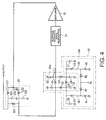
- FIG. 4 is a diagram showing an exemplary specific configuration of the solid-state high-frequency oscillator of FIG. 3.
- the phase shifter 24 is provided with a -3dB90°hybrid coupler 24a, and an addition control section 24b.
- the -3dB90°hybrid coupler 24a is provided with capacitors C1 to C4 and coils L1 to L4.
- the coils L1 to L4 are connected in a loop, and between the coil L1 and the coil L2, the capacitor C1 is connected for connection to the equal divider 2.
- the capacitor C3 is connected, between the coil L3 and the coil L4, the capacitor C4 is connected, and between the coil L4 and the coil L1, the capacitor C2 is connected for connection to the surface acoustic wave resonator 21.
- the addition control section 24b is configured by a reactance adjustable circuit, and is provided with capacitors C5 to C8, coils L5 and L6, resistances R1 and R2, and varactors A1 and A2.
- the capacitor C5, the coil L5, the capacitor C6, the resistances R1 and R2, the capacitor C8, the coil L6, and the capacitor C7 are connected in series in order.
- a terminal between the capacitor C5 and the coil L5 is connected to a terminal between the capacitor C3 and the coil L2 of the -3dB90°hybrid coupler 24a.
- a terminal between the capacitor C7 and the coil L6 is connected to a terminal between the capacitor C4 and the coil L4 of the -3dB90°hybrid coupler 24a.
- the varactor A1 is connected, between the capacitor C8 and the resistance R2, the varactor A2 is connected, and between the resistance R1 and the resistance R2, an input terminal is provided for the control voltage.
- the equal divider 23 serves to equally divide an electric power inside of the oscillator loop for output to the outside of the oscillator loop, and is provided with capacitors C21 to C23, coils L21 and L22, and a resistance R21. Therein, the capacitors C22, the coil L21, the coli L22, and the capacitor C23 are connected in series in this order. Between the coil L21 and the coil L22, the capacitor C21 is connected for connection to the output of the amplifier 22, and between the capacitor C22 and the coil L21, an output terminal of the voltage-controlled oscillator is connected.
- the - 3dB90°hybrid coupler 24a is connected, and between the output terminal of the voltage-controlled oscillator and the - 3dB90°hybrid coupler 24a, the resistance R21 is connected.
- Such a configuration allows to increase the variable width of frequency of the voltage-controlled oscillator, thereby enabling to derive good frequency-variable characteristics with respect to the control voltage. What is more, with low insertion loss, the circuit loss can be also minimized, thereby implementing a voltage-controlled oscillator suffering from less output variation with a high degree of efficiency. Furthermore, the equal divider 23 equally divides an electric power for output to the outside of the oscillator loop without causing impedance disturbance in the oscillator loop, thereby leading to the stable circuit operation with respect to loads.
- FIG. 5 is a cross sectional diagram showing the schematic configuration of a surface acoustic wave resonator according to a fourth embodiment of the invention.
- a thin-film piezoelectric layer 32 is formed on a diamond layer or a diamond-like carbon film layer 31 .
- This thin-film piezoelectric layer 32 is provided thereon with an IDT (Inter Digital Transducer) electrode 33 for exciting the surface acoustic wave, and a reflector electrode for reflecting the surface acoustic wave.
- IDT Inter Digital Transducer
- the thin-film piezoelectric layer 32 can be formed by sputtering, chemical vapour deposition, or others, using ZnO, AlN, Pb(Zr, Ti)O 2 , or others.
- the IDT electrode 33 can be configured by a pair of comb electrodes, which are so placed as to engage with each other.
- the propagation speed is increased in the substrate. This accordingly allows oscillation at higher frequencies, and the IDT electrode 33 can be increased in electrode width compared with any other substrate materials, thereby improving the resistance to electric power. Moreover, the frequency fluctuations can be reduced with respect to any temperature change, thereby implementing an oscillator source with higher precision.
- FIG. 6 is a cross sectional diagram showing the schematic configuration of a surface acoustic wave resonator according to a fifth embodiment of the present invention.
- a semiconductor diamond layer 42 is placed over, and on the semiconductor diamond layer 42, a thin-film piezoelectric layer 43 is formed.
- This thin-film piezoelectric layer 43 is provided thereon with an IDT electrode 43 for exciting the surface acoustic wave, and a reflector electrode for reflecting the surface acoustic wave.
- the semiconductor diamond layer 42 can be formed with an insulation diamond monocrystal material placed between the diamond layer or the diamond-like carbon film layer 41 and the piezoelectric layer 43, by guiding thereto impurities such as B, A1, P, or S, or interstitial defects by ion implantation and electron exposure.
- the IDT electrode 43 may be formed by the semiconductor diamond layer 42.
- the semiconductor diamond layer 42 can configure a thermistor section. This thus allows to detect the temperature of the surface acoustic wave resonator by the thermistor section. By feeding back the detection result to a temperature stabilizing device, the temperature of the surface acoustic wave resonator can be stabilized. As a result, the frequency fluctuations can be reduced with respect to any temperature change, thereby implementing an oscillation circuit with higher precision.
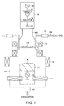
- FIG. 7 is a cross sectional diagram showing the schematic configuration of a semiconductor manufacturing device according to a sixth embodiment of the invention. Note that, in FIG. 7, the semiconductor manufacturing device is exemplified by a plasma etching device for description.
- the plasma etching device is provided with a microwave generator 101.
- the microwave generator 101 is provided with an oscillator 102 for generating a microwave band of high frequency, an amplifier 103 for amplifying the high frequency generated by the oscillator 102, an isolator 104 for blocking reflected wave directed from an object exposed with the microwave, and an antenna 105 that irradiates the microwave.
- the oscillator 102 can generate the frequency of 2.45GHz band for application of plasma generation using the microwave.
- the amplifier 103 can amplify the microwave generated in the oscillator 102 by ion-and-electron separation until deriving the plasma state.
- the plasma etching device is provided with a chamber 107, and the chamber 107 is connected to the microwave generator 101 via a waveguide 106.
- the waveguide 106 is provided therein with a microwave guiding window 110 for guiding the microwave to the chamber 107.
- the chamber 107 is provided therein with a placement base 115 for placing thereon a wafer W, and the placement base 115 is connected with an RF power source 116 for application of RF bias.
- the plasma processing device is provided with a waveguide 108 for guiding a reaction gas to the chamber 107, and the waveguide 108 is provided with a gas flow rate controller 109 for controlling the flow rate of the reaction gas.
- the chamber 107 is connected to an evacuation pipe 113 for evacuating the chamber 107.
- the evacuation path in the chamber 107 is provided with a conductance valve 114 for changing the speed of evacuation.
- the chamber 107 is evacuated via the evacuation pipe 113, and when inside of the chamber 107 reaches a predetermined vacuum level, the reaction gas is guided into the chamber 107 via the waveguide 108.
- the microwave generator 101 a high frequency of 2.45GHz is generated, and the high frequency of 2.45GHz generated by the microwave generator 101 is guided through the waveguide 106, and reaches inside of the chamber 107 via the microwave guiding window 110. Then, by the magnetic field generation coils 111 and 112, the magnetic field is generated in the vicinity of the chamber 107. By electron cyclotron resonance, high-density plasma is generated in the chamber 107. Thereafter, to the placement base 115, the RF bias is applied by the RF power source 116 so that the wafer W is subjected to an etching process using a plasma gas.
- the isolator 104 even if the load impedance varies, the output frequency of the microwave can be stably maintained. Therefore, it becomes possible to reduce the burden on the maintenance of the semiconductor manufacturing device, and to stably generate plasma in the chamber 107, thereby increasing the manufacturing quality.
- exemplified for description is the plasma etching device as a semiconductor manufacturing device.
- the plasma etching device is not the only option, and a plasma CVD device is also an option for application.
- exemplified are the high-frequency heating device and the semiconductor manufacturing device.
- applications may be made to the fields of radar equipment, medical equipment, and any other microwave application equipment.
- FIG. 8 is a block diagram showing the schematic configuration of a high-frequency heating device according to a seventh embodiment of the invention.
- the high-frequency heating device is provided with a metal cavity 204, in which an antenna 205 is placed for microwave irradiation.
- the high-frequency heating device is also provided with an oscillator 201, an amplifier 202, and an isolator 203.
- the oscillator 201 generates a microwave band of high frequency, and the amplifier 202 amplifies the high frequency generated by the oscillator 201.
- the isolator 203 blocks reflected wave coming from an object to be exposed with the microwave.
- the high-frequency heating device also includes a progressive wave/reflected wave detection unit 206, a matching unit 207, and an operation unit 208.
- the progressive wave/reflected wave detection unit 206 detects progressive wave power Pf that is directed to the antenna 205, and reflected wave power Pr that is directed back from the antenna 205.
- the matching unit 207 adjusts the impedance matching with the load.
- the operation unit 208 exercises control over the matching unit 207 based on the progressive wave power Pf and the reflected wave power Pr, both detected by the progressive wave/reflected wave detection unit 206.
- the progressive wave/reflected wave detection unit 206 is exemplified by a directional coupler taking charge of separation between progressive wave and reflected wave.
- the amplifier 202 is connected to the stage subsequent to the oscillator 201, and the isolator 203 is connected to the stage subsequent to the amplifier 202.
- the isolator 203 is connected to the antenna 205 via the progressive wave/reflected wave detection unit 206 and the matching unit 207.
- the microwave generated by the oscillator 201 is amplified in the amplifier 202.
- amplified microwave is then forwarded to the antenna 205 after going through the isolator 203, the progressive wave/reflected wave detection unit 206, and the matching unit 207.
- the microwave is irradiated into the metal cavity 204, and vibrates water molecules of a substance placed in the metal cavity 204 so that the substance is heated.
- the progressive wave power Pf to be directed to the antenna 205 and the reflected wave power Pr to be directed back from the antenna 205 are both detected by the progressive wave/reflected wave detection unit 206.
- the operation unit 208 can exercise control over the matching unit 207 in such a manner that the impedance matching is appropriately adjusted with the object substance to be exposed with the microwave.
- FIG. 9 is a block diagram showing the schematic configuration of a high-frequency heating device according to an eighth embodiment of the invention.
- the high-frequency heating device is provided with a metal cavity 304, in which an antenna 305 is placed for microwave irradiation.
- the high-frequency heating device is also provided with an oscillator 301, an amplifier 302, and an isolator 303.
- the oscillator 301 generates a microwave band of high frequency, and the amplifier 302 amplifies the high frequency generated by the oscillator 301.
- the isolator 303 blocks reflected wave coming from an object to be exposed with the microwave.
- the high-frequency heating device also includes a progressive wave/reflected wave detection unit 306, a matching unit 307, and an operation unit 308.
- the progressive wave/reflected wave detection unit 306 detects progressive wave power Pf that is directed to the antenna 305, and reflected wave power Pr that is directed back from the antenna 305.
- the matching unit 307 adjusts the impedance matching with the load.
- the operation unit 308 exercises control over the amplifier 302 and the matching unit 307 based on the progressive wave power Pf and the reflected wave power Pr, both detected by the progressive wave/reflected wave detection unit 306.
- the progressive wave power Pf to be directed to the antenna 305 and the reflected wave power Pr to be directed back from the antenna 305 are both detected by the progressive wave/reflected wave detection unit 306.
- the operation unit 308 can exercise control over the matching unit 307 in such a manner that the impedance matching is appropriately adjusted with the object substance to be exposed with the microwave, and over the amplification level of the amplifier 302 in such a manner that the object can absorb the microwave with efficiency.
- This configuration enables to exercise control over the microwave coming from the antenna while monitoring the reflected wave power Pr, which varies depending on the object's position, object's size, temperature, permittivity, conductivity, and others. Accordingly, such factors as object's position, object's size, temperature, permittivity, conductivity, and others are used as a basis to apply power control so as to help the object to absorb the microwave with efficiency. As such, the object can be heated while measures are taken to ensure power conservation and short time operation.
- FIG. 10 is a block diagram showing the schematic configuration of a high-frequency heating device according to a ninth embodiment of the invention.
- the high-frequency heating device is provided with a metal cavity 404, in which an antenna 405 is placed for microwave irradiation.
- the high-frequency heating device is also provided with an oscillator 401, an amplifier 402, and an isolator 403.
- the oscillator 401 generates a microwave band of high frequency, and the amplifier 402 amplifies the high frequency generated by the oscillator 401.
- the isolator 403 blocks reflected wave coming from an object to be exposed with the microwave.
- the high-frequency heating device also includes a progressive wave/reflected wave detection unit 406, a matching unit 407, and an operation unit 408.
- the progressive wave/reflected wave detection unit 406 detects progressive wave power Pf that is directed to the antenna 405, and reflected wave power Pr that is directed back from the antenna 405.
- the matching unit 407 adjusts the impedance matching with the load.
- the operation unit 408 exercises control over oscillator 401 and the matching unit 407 based on the progressive wave power Pf and the reflected wave power Pr, both detected by the progressive wave/reflected wave detection unit 406.
- the progressive wave power Pf to be directed to the antenna 405 and the reflected wave power Pr to be directed back from the antenna 405 are both detected by the progressive wave/reflected wave detection unit 406.
- the operation unit 408 can exercise control over the matching unit 407 in such a manner that the impedance matching is appropriately adjusted with the object substance to be exposed with the microwave, and over the oscillation frequency of the oscillator 401 in such a manner as to achieve the maximum efficiency, or the minimum time or power.
- FIG. 11 is a block diagram showing the schematic configuration of a high-frequency heating device according to a tenth embodiment of the invention.
- the high-frequency heating device is provided with a metal cavity 504, in which an antenna 505 is placed for microwave irradiation.
- the high-frequency heating device is also provided with an oscillator 501, an amplifier 502, and an isolator 503.
- the oscillator 501 generates a microwave band of high frequency, and the amplifier 502 amplifies the high frequency generated by the oscillator 501.
- the isolator 503 blocks reflected wave coming from an object to be exposed with the microwave.
- the high-frequency heating device also includes a progressive wave/reflected wave detection unit 506 a matching unit 507, and an operation unit 508.
- the progressive wave/reflected wave detection unit 506 detects progressive wave power Pf that is directed to the antenna 505, and reflected wave power Pr that is directed back from the antenna 505.
- the matching unit 507 adjusts the impedance matching with the load.
- the operation unit 508 exercises control over the oscillator 501, the amplifier 502, and the matching unit 507 based on the progressive wave power Pf and the reflected wave power Pr, both detected by the progressive wave/reflected wave detection unit 506.
- the progressive wave power Pf to be directed to the antenna 505 and the reflected wave power Pr to be directed back from the antenna 505 are both detected by the progressive wave/reflected wave detection unit 506.
- the operation unit 508 can exercise control over the matching unit 507 in such a manner that the impedance matching is appropriately adjusted with the object substance to be exposed with the microwave.
- the operation unit 508 is also in charge of changing the amplification level of the amplifier 502 in such a manner as to maximize the efficiency or minimize the time, or controlling the oscillation frequency of the oscillator 501 in such a manner as to maximize the efficiency, or minimize the time or power.
- FIG. 12 is a block diagram showing the schematic configuration of a high-frequency heating device according to an eleventh embodiment of the invention.
- the high-frequency heating device is provided with a metal cavity 604, in which antennas 605a and 605b are placed for microwave irradiation.
- the high-frequency heating device is also provided with an oscillator 601, an amplifier 602, and an isolator 603.
- the oscillator 601 generates a microwave band of high frequency
- the amplifier 602 amplifies the high frequency generated by the oscillator 601.
- the isolator 603 blocks reflected wave coming from an object to be exposed with the microwave.
- the high-frequency heating device also includes progressive wave/reflected wave detection units 606a and 606b, matching units 607a and 607b, and an operation unit 608.
- the progressive wave/reflected wave detection units 606a and 606b respectively detect progressive wave power Pf1 and Pf2 that are directed to the corresponding antenna 605a or 605b, and reflected wave powers Pr1 and Pr2 that are directed back from the corresponding antenna 605a or 605b.
- the matching units 607a and 607b both adjust the impedance matching with the load of being exposed with the microwave coming from the antennas 605a and 605b.
- the operation unit 608 exercises control over the oscillator 601, the amplifier 602, and the matching units 607a and 607b based on the progressive wave powers Pf1 and Pf2, and the reflected wave powers Pr1 and Pr2, detected by the corresponding progressive wave/reflected wave detection unit 606a or 606b.
- a power splitter 609 is provided that is in charge of power allocation to the antennas 605a and 605b.
- the progressive wave powers Pf1 and Pf2 to be directed to the antennas 605a and 605b and the reflected wave powers Pr1 and Pr2 to be directed back from the antennas 605a and 605b are detected by the corresponding progressive wave/reflected wave detection unit 606a or 606b.
- the operation units 608 can exercise control over the matching units 607a and 607b in such a manner that the impedance matching is appropriately adjusted with the object to be exposed with the microwave.
- the operation unit 608 also in charge of changing the amplification level of the amplifier 602 in such a manner as to maximize the efficiency or minimize the time, or controlling the oscillation frequency of the oscillator 601 in such a manner as to maximize the efficiency, or minimize the time or power.
- the microwave can be uniformly irradiated into the metal cavity 604 so that the object can be uniformly heated to a greater degree.
- the antennas 5, 105, 205, 305, 405, 505, 605a, and 605b are preferably a unidirectional planar antenna, e.g., patch antenna or slot antenna, or a phased array antenna.
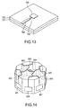
- FIG. 13 is a perspective view showing the schematic configuration of a single patch antenna to be applied to the invention.
- a dielectric material 702 is formed thereon with conductor patterns 703 to 705, and the underside thereof is formed with a conductor layer 701.
- the conductor patterns 703 to 705 can configure a microstrip line.
- the conductor pattern 705 configures a planar antenna, and with length and width adjustment for the conductor patterns 703 and 704, the impedance matching can be achieved.
- This configuration favorably reduces the size of the antennas 5, 105, 205, 305, 405, 505, 605a, and 605b for use with high-frequency heating devices, and the antenna 105 for use with semiconductor manufacturing devices.
- the configuration also reduces the size and weight of the metal cavities 4, 204, 304, 404, 504, and 604, and the chamber 101.
- the directivity thereof can be well matched to the object in the metal cavities 4, 204, 304, 404, 504, and 604, and in the chamber 101, thereby enabling efficient microwave irradiation to the object.
- FIG. 14 is a perspective view showing the schematic configuration of a complex patch antenna to be applied to the invention.
- single patch antennas 801 to 808 are so placed as to configure an octagonal column.
- the single patch antennas 801 to 808 are connected together via a wiring pattern 809. Note here that such single patch antennas 801 to 808 are each exemplified by the single patch antenna of FIG. 13.
- the microwave can be directed centrally so that the object can be exposed with the microwave with efficiency.
- FIG. 15 is a diagram showing the schematic configuration of a phased array antenna to be applied to the invention.
- a metal cavity 903 carries therein a plurality of antennas 902a to 902f for microwave irradiation.
- the antennas 902a to 902f are connected with phase shifters 901 to 901f, respectively.
- the phase shifters 901a to 901f are in charge of adjusting the progressive power by phase before transmission to the antennas 902a to 902f, thereby controlling the directivity of the microwave.
- the microwave can be directed in the direction of the object, or the microwave can be available for scanning.
- Using the phased array antenna allows electrical phase control, and thus the directivity can be changed at a high speed.
- the antenna in combination with a voltage-control SAW oscillator having a high degree of high-speed modulation characteristic, the antenna can afford better control over the high-speed directivity so that the temperature-varying object can be heated as appropriate, and plasma generation can be controlled in the right place at the right time.
- the antenna 902a to 902f may take one-dimensional or two-dimensional configuration for placement. Assuming that the antennas 902a to 902f are arranged two-dimensionally, the microwave can be changed in directivity on a two-dimensional plane, right and left and top and bottom.
- FIG. 16 is a diagram showing a modulation method for a microwave output according to an embodiment of the invention.
- the microwave output in a case of controlling the microwave output for irradiation to the object, can be subjected to FSK modulation or ASK modulation so as to minimize the reflected wave power, or the oscillation output can be subjected to On/Off control.
- the amplification level is so changed as to maximize the efficiency or minimize the time, and the object is so heated as to maximize the efficiency, or minimize the time or power through FSK modulation or ASK modulation applied to the microwave output.
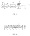
- FIG. 17 is a block diagram showing the schematic configuration of a light source device according to a twelfth embodiment of the invention.
- the light source device is provided with a glass tube 1004 with a bulging portion 1006, in which an antenna 1005 is placed for microwave irradiation.
- the light source device is also provided with a metal mesh 1007 along the surface of the bulging portion 1006 for reflecting the microwave coming from the antenna 1005.
- the glass tube 1004 can be filled with a noble gas such as argon gas, neon gas, halogen gas, xenon gas, or others.
- the light source device is also provided with an oscillator 1001, an amplifier 1002, and an isolator 1003.
- the oscillator 1001 generates a microwave band of high frequency
- the amplifier 1002 amplifies the high frequency generated by the oscillator 1001.
- the isolator 1003 blocks reflected wave coming from an object to be exposed with the microwave.
- the amplifier 1002 is connected to the stage subsequent to the oscillator 1001, and the isolator 1003 is connected to the stage subsequent to the amplifier 1002.
- the isolator 1003 is connected to the antenna 1005.
- the microwave generated by the oscillator 1001 is amplified by the amplifier 1002.
- amplified microwave is then forwarded to the antenna 1005 after going through the isolator 1003.
- the microwave is irradiated into the glass tube 1004, and excites the noble gas filled in the glass tube 1004 for light emission.
- This configuration eliminates the need to use a magnetron to generate the microwave band of high frequency, and the need to use a filament for light emission. Accordingly, the light intensity and the spectral characteristics can be highly stable for a long period of time, and the reflected wave coming from the object having been exposed with the microwave is prevented from directing back to the amplifier so that the amplifier is protected from damage.
- the light source device of FIG. 17 is applicable to luminaries for air-traffic control that are expected to be highly reliable, luminaries for steel towers, railroad bridges, tunnels or others that are difficult to maintain, vehicle headlights or headlamps for aerospace use that are supposed to withstand large acceleration forces and vibrations, light sources for ultraviolet sterilization, variable-flash-at-a-high-speed displays for general types of moving images, or others.
- the antenna 1005 of FIG. 17 may be the single patch antenna of FIG. 13, the complex patch antenna of FIG. 14, or the phased array antenna of FIG. 15. Moreover, the configurations of FIGS. 8 to 12 may be applied to the light source device of FIG. 17.
- the oscillator 1001 may be the SAW oscillator of FIG. 5, 6, or 18.
- FIG. 18 is a cross sectional diagram showing the schematic configuration of a surface acoustic wave resonator according to a thirteenth embodiment of the invention.
- a silicon substrate 1011 is formed thereon with a diamond layer 1012, and on the diamond layer 1012, a ZnO film 1013 is formed.
- the diamond layer 1012 may be of monocrystalline or polycrystalline, or a hard carbon film having an elastic constant close to that of the diamond layer 1012 may be used as an alternative to the diamond layer 1012.
- the ZnO film 1013 is formed thereon with an IDT electrode 1014 for excitation of the surface acoustic wave, and a reflector electrode for reflection of the surface acoustic wave.
- an SiO 2 film 1015 is so placed as to cover the IDT electrode 1014.
- the SiO 2 layer 1015 becomes able to take charge of temperature compensation with respect to the ZnO film 1013. This thus helps suppress the frequency fluctuations occurring to a SAW oscillator as a result of temperature variation, thereby stabilizing the microwave output.
Landscapes
- Physics & Mathematics (AREA)
- Engineering & Computer Science (AREA)
- Plasma & Fusion (AREA)
- Chemical & Material Sciences (AREA)
- Analytical Chemistry (AREA)
- Electromagnetism (AREA)
- Health & Medical Sciences (AREA)
- Clinical Laboratory Science (AREA)
- General Health & Medical Sciences (AREA)
- Plasma Technology (AREA)
- Control Of High-Frequency Heating Circuits (AREA)
- Circuit Arrangements For Discharge Lamps (AREA)
- Non-Portable Lighting Devices Or Systems Thereof (AREA)
- Drying Of Semiconductors (AREA)
- Constitution Of High-Frequency Heating (AREA)
Applications Claiming Priority (2)
| Application Number | Priority Date | Filing Date | Title |
|---|---|---|---|
| JP2004289638 | 2004-10-01 | ||
| JP2005212297A JP2006128075A (ja) | 2004-10-01 | 2005-07-22 | 高周波加熱装置、半導体製造装置および光源装置 |
Publications (2)
| Publication Number | Publication Date |
|---|---|
| EP1643641A2 true EP1643641A2 (de) | 2006-04-05 |
| EP1643641A3 EP1643641A3 (de) | 2006-05-31 |
Family
ID=35636891
Family Applications (1)
| Application Number | Title | Priority Date | Filing Date |
|---|---|---|---|
| EP05021264A Withdrawn EP1643641A3 (de) | 2004-10-01 | 2005-09-29 | Hochfrequenz-Heizvorrichtung, Halbleiterfabrikationsvorrichtung, und Lichtquellevorrichtung |
Country Status (4)
| Country | Link |
|---|---|
| US (1) | US7554054B2 (de) |
| EP (1) | EP1643641A3 (de) |
| JP (1) | JP2006128075A (de) |
| KR (1) | KR100741220B1 (de) |
Cited By (20)
| Publication number | Priority date | Publication date | Assignee | Title |
|---|---|---|---|---|
| US20080266012A1 (en) * | 2007-04-25 | 2008-10-30 | Kazuhiro Yahata | Method for controlling high-frequency radiator |
| EP2205043A4 (de) * | 2007-10-18 | 2011-03-23 | Panasonic Corp | Mikrowellenheizvorrichtung |
| EP2469975A1 (de) * | 2010-12-21 | 2012-06-27 | Whirlpool Corporation | Steuerung der Mikrowellenquellenwirksamkeit in einer Mikrowellenheizvorrichtung |
| EP2469974A1 (de) * | 2010-12-21 | 2012-06-27 | Whirlpool Corporation | Verfahren zum Steuern der Kühlung in einer Mikrowellen-Heizvorrichtung und Vorrichtung dafür |
| WO2012084658A1 (en) * | 2010-12-23 | 2012-06-28 | Element Six Limited | Microwave power delivery system for plasma reactors |
| WO2012146870A1 (fr) | 2011-04-27 | 2012-11-01 | Sairem Societe Pour L'application Industrielle De La Recherche En Electronique Et Micro Ondes | Installation de traitement micro-onde d'une charge |
| US8859058B2 (en) | 2010-12-23 | 2014-10-14 | Element Six Limited | Microwave plasma reactors and substrates for synthetic diamond manufacture |
| EP2549832A4 (de) * | 2010-03-19 | 2014-11-05 | Panasonic Corp | Mirkowellenerhitzungsvorrichtung |
| US8955456B2 (en) | 2010-12-23 | 2015-02-17 | Element Six Limited | Microwave plasma reactor for manufacturing synthetic diamond material |
| CN105492831A (zh) * | 2013-08-29 | 2016-04-13 | 飞思卡尔半导体公司 | 集成固态微波功率发生模块 |
| US9410242B2 (en) | 2010-12-23 | 2016-08-09 | Element Six Technologies Limited | Microwave plasma reactor for manufacturing synthetic diamond material |
| EP3073803A1 (de) | 2015-03-25 | 2016-09-28 | Topinox Sarl | Verfahren zur steuerung eines mikrowellen-gargeräts sowie mikrowellen-gargerät |
| DE102015109070A1 (de) * | 2015-06-09 | 2016-12-15 | Topinox Sarl | Verfahren zur Steuerung eines Mikrowellen-Gargeräts sowie Gargerät mit einem Mikrowellengenerator |
| US9637838B2 (en) | 2010-12-23 | 2017-05-02 | Element Six Limited | Methods of manufacturing synthetic diamond material by microwave plasma enhanced chemical vapor deposition from a microwave generator and gas inlet(s) disposed opposite the growth surface area |
| CN107181056A (zh) * | 2017-05-16 | 2017-09-19 | 叶云裳 | 一种微波衰减型高稳相、高精度gnss测量型天线及设备 |
| US10403477B2 (en) | 2010-12-23 | 2019-09-03 | Element Six Technologies Limited | Microwave plasma reactor for manufacturing synthetic diamond material |
| US11316495B2 (en) | 2017-11-15 | 2022-04-26 | Huawei Technologies Co., Ltd. | Surface acoustic wave device |
| US11371147B2 (en) | 2010-12-23 | 2022-06-28 | Element Six Technologies Limited | Microwave plasma reactor for manufacturing synthetic diamond material |
| US11764731B2 (en) * | 2020-02-21 | 2023-09-19 | STMicroelectronics (Alps) SAS | Drift compensation |
| WO2025228785A1 (de) * | 2024-04-29 | 2025-11-06 | TRUMPF Hüttinger GmbH + Co. KG | Verfahren zum einstellen einer hochfrequenz-leistungsverteilung, phasengesteuerter hybridkoppler, hybridkoppler-system und hybridkoppler-anordnung |
Families Citing this family (99)
| Publication number | Priority date | Publication date | Assignee | Title |
|---|---|---|---|---|
| CN100562700C (zh) * | 2004-04-12 | 2009-11-25 | 财团法人北九州产业学术推进机构 | 使用微波的减压干燥方法及其装置 |
| US7164095B2 (en) * | 2004-07-07 | 2007-01-16 | Noritsu Koki Co., Ltd. | Microwave plasma nozzle with enhanced plume stability and heating efficiency |
| US20060052883A1 (en) * | 2004-09-08 | 2006-03-09 | Lee Sang H | System and method for optimizing data acquisition of plasma using a feedback control module |
| JP2007095452A (ja) * | 2005-09-28 | 2007-04-12 | Seiko Epson Corp | 発光装置 |
| JP2007096645A (ja) * | 2005-09-28 | 2007-04-12 | Seiko Epson Corp | マイクロ波発生装置およびこれを用いた機器 |
| US7816871B2 (en) * | 2005-11-01 | 2010-10-19 | Seiko Epson Corporation | Projector and method of turning on light source device of projector |
| US7795815B2 (en) * | 2005-11-01 | 2010-09-14 | Seiko Epson Corporation | Light source device and projector including light source device |
| US20070103645A1 (en) * | 2005-11-01 | 2007-05-10 | Seiko Epson Corporation | Projector |
| TW200742506A (en) * | 2006-02-17 | 2007-11-01 | Noritsu Koki Co Ltd | Plasma generation apparatus and work process apparatus |
| JP4935188B2 (ja) * | 2006-05-25 | 2012-05-23 | パナソニック株式会社 | マイクロ波利用装置 |
| JP5023569B2 (ja) * | 2006-06-21 | 2012-09-12 | パナソニック株式会社 | 衣類乾燥機 |
| JP5111806B2 (ja) * | 2006-08-02 | 2013-01-09 | 東京エレクトロン株式会社 | プラズマ処理装置と方法 |
| JP5064924B2 (ja) * | 2006-08-08 | 2012-10-31 | パナソニック株式会社 | マイクロ波処理装置 |
| US8280323B2 (en) * | 2006-10-11 | 2012-10-02 | Bae Systems Information And Electronic Systems Integration Inc. | Fuzzy logic control of an RF power amplifier for automatic self-tuning |
| JP4967600B2 (ja) * | 2006-10-24 | 2012-07-04 | パナソニック株式会社 | マイクロ波処理装置 |
| JP4215107B2 (ja) | 2007-02-02 | 2009-01-28 | セイコーエプソン株式会社 | 光源装置、プロジェクタ |
| JP5167678B2 (ja) * | 2007-04-16 | 2013-03-21 | パナソニック株式会社 | マイクロ波処理装置 |
| JP5142364B2 (ja) * | 2007-07-05 | 2013-02-13 | パナソニック株式会社 | マイクロ波処理装置 |
| JP4629085B2 (ja) * | 2007-11-27 | 2011-02-09 | パナソニック株式会社 | 加熱調理器 |
| JP5127038B2 (ja) * | 2007-12-03 | 2013-01-23 | パナソニック株式会社 | 高周波処理装置 |
| JP5169255B2 (ja) * | 2008-01-29 | 2013-03-27 | パナソニック株式会社 | マイクロ波処理装置 |
| US7803274B2 (en) * | 2008-04-30 | 2010-09-28 | Celgard Llc | Contained liquid membrane contactor and a method of manufacturing the same |
| US20100051612A1 (en) * | 2008-08-29 | 2010-03-04 | Hans Magnus Fagrell | Microwave heater and method of heating |
| JP5358580B2 (ja) * | 2008-09-17 | 2013-12-04 | パナソニック株式会社 | マイクロ波加熱装置 |
| US20100074810A1 (en) * | 2008-09-23 | 2010-03-25 | Sang Hun Lee | Plasma generating system having tunable plasma nozzle |
| US8188904B2 (en) * | 2008-10-09 | 2012-05-29 | Infineon Technologies Ag | RF circuit with improved antenna matching |
| US7921804B2 (en) * | 2008-12-08 | 2011-04-12 | Amarante Technologies, Inc. | Plasma generating nozzle having impedance control mechanism |
| US20100201272A1 (en) * | 2009-02-09 | 2010-08-12 | Sang Hun Lee | Plasma generating system having nozzle with electrical biasing |
| US20100254853A1 (en) * | 2009-04-06 | 2010-10-07 | Sang Hun Lee | Method of sterilization using plasma generated sterilant gas |
| KR101637880B1 (ko) * | 2009-06-19 | 2016-07-08 | 엘지전자 주식회사 | 마이크로웨이브를 이용한 조리기기 |
| US9398646B2 (en) * | 2009-07-10 | 2016-07-19 | Panasonic Intellectual Property Management Co., Ltd. | Microwave heating device and microwave heating control method |
| US9491811B2 (en) * | 2009-07-21 | 2016-11-08 | Lg Electronics Inc. | Cooking appliance employing microwaves |
| WO2011052653A1 (ja) * | 2009-10-29 | 2011-05-05 | 日本電業工作株式会社 | 電力回生装置および電力回生方法、電力蓄電システムおよび電力蓄電方法、ならびに高周波装置 |
| JP5471515B2 (ja) * | 2010-01-28 | 2014-04-16 | パナソニック株式会社 | マイクロ波処理装置 |
| KR101752523B1 (ko) * | 2010-07-01 | 2017-06-29 | 고지 엘티디. | 무선 주파수 에너지에 의한 대상물 처리 |
| US9992824B2 (en) | 2010-10-29 | 2018-06-05 | Goji Limited | Time estimation for energy application in an RF energy transfer device |
| JP2012109080A (ja) * | 2010-11-16 | 2012-06-07 | Tokyo Electron Ltd | プラズマ処理装置およびプラズマ処理方法 |
| CN102284265B (zh) * | 2011-06-10 | 2014-03-12 | 宁波大学 | 一种以声表面波为能量源的微反应器及其反应方法 |
| CN102350285B (zh) * | 2011-07-11 | 2014-01-22 | 宁波大学 | 一种以声表面波为能量源的微反应器及其反应方法 |
| US9585203B2 (en) * | 2011-08-04 | 2017-02-28 | Panasonic Intellectual Property Management Co., Ltd. | Microwave heating device |
| US20130080098A1 (en) | 2011-08-31 | 2013-03-28 | Goji, Ltd. | Object Processing State Sensing Using RF Radiation |
| DE102011055624A1 (de) * | 2011-11-23 | 2013-05-23 | Dritte Patentportfolio Beteiligungsgesellschaft Mbh & Co.Kg | HF-System |
| EP2677839A1 (de) * | 2012-06-18 | 2013-12-25 | Whirlpool Corporation | Mikrowellenwärmvorrichtung mit mehreren Einspeisepunkten |
| US11786146B1 (en) | 2012-09-25 | 2023-10-17 | Micro Mobio Corporation | Wireless hub system and method |
| US11058326B1 (en) * | 2012-09-25 | 2021-07-13 | Micro Mobio Corporation | Cloud communication antenna panel system and method |
| US12138041B1 (en) | 2012-09-25 | 2024-11-12 | Micro Mobio Corporation | Mobile device case with satellite communication capability |
| JP6067428B2 (ja) * | 2013-03-07 | 2017-01-25 | 株式会社東芝 | マイクロ波加熱装置及び排気ガス浄化装置 |
| FR3005167B1 (fr) * | 2013-04-30 | 2016-09-30 | Senseor | Systeme d'interrogation d'un capteur passif interrogeable a distance integre dans une cavite metallique a bilan energetique optimise et procede d'interrogation |
| CN103325961B (zh) * | 2013-05-22 | 2016-05-18 | 上海和辉光电有限公司 | Oled封装加热装置及工艺方法 |
| US9129918B2 (en) | 2013-10-30 | 2015-09-08 | Taiwan Semiconductor Manufacturing Company Limited | Systems and methods for annealing semiconductor structures |
| US20150136760A1 (en) * | 2013-11-15 | 2015-05-21 | Stmicroelectronics (Canada), Inc. | Microwave oven using solid state amplifiers and antenna array |
| WO2015139464A1 (zh) * | 2014-03-20 | 2015-09-24 | 广东美的厨房电器制造有限公司 | 微波炉的半导体微波发生器连接结构、微波炉的半导体微波发生器输入输出连接结构和微波炉 |
| CN203797741U (zh) * | 2014-04-24 | 2014-08-27 | 广东美的厨房电器制造有限公司 | 微波炉 |
| WO2016104098A1 (ja) | 2014-12-25 | 2016-06-30 | 東京エレクトロン株式会社 | プラズマ処理装置およびプラズマ処理方法 |
| EP3337944B1 (de) * | 2015-08-20 | 2020-01-08 | VKR Holding A/S | Evakuierungskopf mit keramischer heizung zur herstellung einer vig-einheit |
| KR102336430B1 (ko) * | 2015-10-21 | 2021-12-08 | 삼성전자주식회사 | 저주파 자기장 기반 가열 장치 및 방법 |
| CN105423363B (zh) * | 2016-01-06 | 2018-03-16 | 广东美的厨房电器制造有限公司 | 微波源系统、微波炉及在微波源系统中执行的方法 |
| US10638559B2 (en) * | 2016-06-30 | 2020-04-28 | Nxp Usa, Inc. | Solid state microwave heating apparatus and method with stacked dielectric resonator antenna array |
| US10531526B2 (en) * | 2016-06-30 | 2020-01-07 | Nxp Usa, Inc. | Solid state microwave heating apparatus with dielectric resonator antenna array, and methods of operation and manufacture |
| EP3280225B1 (de) | 2016-08-05 | 2020-10-07 | NXP USA, Inc. | Abtauvorrichtung mit konzentriertem induktivem anpassungsnetzwerk und verfahren zum betrieb davon |
| EP3280224A1 (de) | 2016-08-05 | 2018-02-07 | NXP USA, Inc. | Vorrichtung und verfahren zur erkennung der beendigung des abtaubetriebs |
| US10748745B2 (en) * | 2016-08-16 | 2020-08-18 | Applied Materials, Inc. | Modular microwave plasma source |
| US10602573B2 (en) | 2016-11-18 | 2020-03-24 | Nxp Usa, Inc. | Establishing RF excitation signal parameters in a solid-state heating apparatus |
| WO2018123249A1 (ja) * | 2016-12-27 | 2018-07-05 | 株式会社日立国際電気 | マイクロ波加熱処理装置及び炭素繊維の製造装置と製造方法 |
| US9849708B1 (en) * | 2017-02-23 | 2017-12-26 | Ricoh Company, Ltd. | Microwave dryer of a print system with modulation of the microwave source using frequency shift keying |
| US10707058B2 (en) | 2017-04-11 | 2020-07-07 | Applied Materials, Inc. | Symmetric and irregular shaped plasmas using modular microwave sources |
| US10412795B2 (en) | 2017-04-28 | 2019-09-10 | Nxp Usa, Inc. | Power measurement via bond wire coupling |
| US11037764B2 (en) | 2017-05-06 | 2021-06-15 | Applied Materials, Inc. | Modular microwave source with local Lorentz force |
| CN118315255A (zh) * | 2017-08-14 | 2024-07-09 | 株式会社国际电气 | 等离子体生成装置 |
| US10648728B2 (en) | 2017-09-29 | 2020-05-12 | Nxp Usa, Inc. | Multifunctional radio frequency systems and methods for UV sterilization, air purification, and defrost operations |
| US11160145B2 (en) | 2017-09-29 | 2021-10-26 | Nxp Usa, Inc. | Drawer apparatus for radio frequency heating and defrosting |
| US10917948B2 (en) | 2017-11-07 | 2021-02-09 | Nxp Usa, Inc. | Apparatus and methods for defrosting operations in an RF heating system |
| US10771036B2 (en) | 2017-11-17 | 2020-09-08 | Nxp Usa, Inc. | RF heating system with phase detection for impedance network tuning |
| US10785834B2 (en) | 2017-12-15 | 2020-09-22 | Nxp Usa, Inc. | Radio frequency heating and defrosting apparatus with in-cavity shunt capacitor |
| EP3503679B1 (de) | 2017-12-20 | 2022-07-20 | NXP USA, Inc. | Abtauvorrichtung und verfahren zum betrieb davon |
| CN108668395B (zh) | 2017-12-29 | 2022-03-04 | 恩智浦美国有限公司 | 用于rf加热系统的平面电感器 |
| EP3547801B1 (de) | 2018-03-29 | 2022-06-08 | NXP USA, Inc. | Abtauvorrichtung und verfahren zum betrieb davon |
| US11081317B2 (en) | 2018-04-20 | 2021-08-03 | Applied Materials, Inc. | Modular high-frequency source |
| US10504699B2 (en) * | 2018-04-20 | 2019-12-10 | Applied Materials, Inc. | Phased array modular high-frequency source |
| US11393661B2 (en) | 2018-04-20 | 2022-07-19 | Applied Materials, Inc. | Remote modular high-frequency source |
| CN112469945A (zh) * | 2018-07-31 | 2021-03-09 | 松下知识产权经营株式会社 | 高频加热装置 |
| US10952289B2 (en) | 2018-09-10 | 2021-03-16 | Nxp Usa, Inc. | Defrosting apparatus with mass estimation and methods of operation thereof |
| US11800608B2 (en) | 2018-09-14 | 2023-10-24 | Nxp Usa, Inc. | Defrosting apparatus with arc detection and methods of operation thereof |
| US11723121B2 (en) | 2018-09-14 | 2023-08-08 | Nxp Usa, Inc. | Defrosting apparatus with low-loss load detection and methods of operation thereof |
| US11484048B2 (en) | 2018-09-14 | 2022-11-01 | Nxp Usa, Inc. | Defrosting apparatus with defrosting operation monitoring and methods of operation thereof |
| CN109259045A (zh) | 2018-10-19 | 2019-01-25 | 恩智浦美国有限公司 | 具有可重新定位电极的解冻设备 |
| US11089661B2 (en) | 2018-12-14 | 2021-08-10 | Nxp Usa, Inc. | Defrosting apparatus with repositionable electrodes |
| US11166352B2 (en) | 2018-12-19 | 2021-11-02 | Nxp Usa, Inc. | Method for performing a defrosting operation using a defrosting apparatus |
| US11013075B2 (en) | 2018-12-20 | 2021-05-18 | Nxp Usa, Inc. | RF apparatus with arc prevention using non-linear devices |
| US11229094B2 (en) | 2018-12-20 | 2022-01-18 | Nxp Usa, Inc. | Combined RF and thermal heating system and methods of operation thereof |
| US11039511B2 (en) | 2018-12-21 | 2021-06-15 | Nxp Usa, Inc. | Defrosting apparatus with two-factor mass estimation and methods of operation thereof |
| US11324082B2 (en) | 2019-05-02 | 2022-05-03 | Nxp Usa, Inc. | RF thermal increase systems with multi-level electrodes |
| US11324084B2 (en) | 2019-05-16 | 2022-05-03 | Nxp Usa, Inc. | Combined RF and thermal heating system with heating time estimation |
| JP2021007133A (ja) * | 2019-06-28 | 2021-01-21 | 東京エレクトロン株式会社 | 加熱装置、加熱方法、および基板処理装置 |
| KR102812188B1 (ko) * | 2021-09-08 | 2025-05-27 | 세메스 주식회사 | 기판 처리 장치 및 기판 처리 방법 |
| US20230133484A1 (en) * | 2021-10-29 | 2023-05-04 | Intel Corporation | Interconnects with liner that resonates during microwave anneal |
| CN120419285A (zh) * | 2023-01-10 | 2025-08-01 | 松下知识产权经营株式会社 | 信号输出装置、微波炉、冰箱和冷冻机 |
| EP4661595A4 (de) * | 2023-02-02 | 2026-04-29 | Panasonic Ip Man Co Ltd | Funkwellen-emissionseinrichtung |
| US20250043413A1 (en) * | 2023-07-31 | 2025-02-06 | Applied Materials, Inc. | Microwave plasma chemical vapor deposition of nanocrystalline diamond film |
Family Cites Families (50)
| Publication number | Priority date | Publication date | Assignee | Title |
|---|---|---|---|---|
| US3953702A (en) * | 1974-08-13 | 1976-04-27 | Texas Instruments Incorporated | Solid state microwave oven power source |
| US3943403A (en) * | 1975-04-21 | 1976-03-09 | Gte Laboratories Incorporated | Electrodeless light source utilizing a lamp termination fixture having parallel capacitive impedance matching capability |
| US4070603A (en) * | 1976-07-14 | 1978-01-24 | Gte Laboratories Incorporated | Solid state microwave power source for use in an electrodeless light source |
| CA1081796A (en) * | 1978-02-09 | 1980-07-15 | Canadian Patents And Development Limited | Controlled heating microwave ovens using different operating frequencies |
| US4210795A (en) * | 1978-11-30 | 1980-07-01 | Litton Systems, Inc. | System and method for regulating power output in a microwave oven |
| CA1202090A (en) * | 1982-09-20 | 1986-03-18 | Hisashi Okatsuka | Microwave heating apparatus with solid state microwave oscillating device |
| US4460814A (en) * | 1982-09-27 | 1984-07-17 | Amana Refrigeration, Inc. | Oven antenna probe for distributing energy in microwave |
| US5109203A (en) * | 1986-04-24 | 1992-04-28 | Energy Compression Research Corp. | Generated and method for generating microwaves |
| DE3743921A1 (de) * | 1987-12-23 | 1989-07-13 | Bosch Siemens Hausgeraete | Steueranordnung zum waermetechnischen behandeln von lebensmitteln durch mikrowellenenergie |
| US4871984A (en) * | 1988-06-24 | 1989-10-03 | Raytheon Company | Surface acoustic wave oscillator |
| US5179264A (en) | 1989-12-13 | 1993-01-12 | International Business Machines Corporation | Solid state microwave powered material and plasma processing systems |
| US5961871A (en) * | 1991-11-14 | 1999-10-05 | Lockheed Martin Energy Research Corporation | Variable frequency microwave heating apparatus |
| JPH0546111U (ja) * | 1991-11-21 | 1993-06-18 | 三菱電機株式会社 | 弾性表面波発振器 |
| JPH05152216A (ja) * | 1991-11-29 | 1993-06-18 | Hitachi Ltd | プラズマ処理装置 |
| US5280217A (en) * | 1992-08-14 | 1994-01-18 | Gte Products Corporation | Apparatus for coupling energy to electrodeless lamp applicators |
| JP3252865B2 (ja) * | 1992-09-11 | 2002-02-04 | 住友電気工業株式会社 | 表面弾性波素子および表面弾性波素子の製造方法 |
| JP3205976B2 (ja) * | 1992-09-14 | 2001-09-04 | 住友電気工業株式会社 | 表面弾性波素子 |
| US5313144A (en) * | 1992-12-31 | 1994-05-17 | Osram Sylvania Inc. | Power balanced coupling structure for electrodeless discharge lamp |
| JPH07130463A (ja) * | 1993-10-28 | 1995-05-19 | New Japan Radio Co Ltd | 電子レンジ |
| JPH087610A (ja) | 1994-06-16 | 1996-01-12 | Fujitsu Ltd | 光源装置及び投射型表示装置 |
| JP3173362B2 (ja) | 1996-03-11 | 2001-06-04 | 松下電器産業株式会社 | マイクロ波放電光源装置 |
| US6137237A (en) * | 1998-01-13 | 2000-10-24 | Fusion Lighting, Inc. | High frequency inductive lamp and power oscillator |
| US6111237A (en) * | 1998-04-24 | 2000-08-29 | Cerberus Institute For Research And Development, Inc. | Microwave facilitated atmospheric energy projection system |
| ATE354268T1 (de) * | 1998-12-17 | 2007-03-15 | Biotage Ab | Mikrowellenvorrichtung und verfahren zum durchführen chemischer reaktionen |
| JP2000196329A (ja) | 1998-12-24 | 2000-07-14 | Nec Corp | フェーズドアレイアンテナおよびその製造方法 |
| JP2001202923A (ja) | 2000-01-19 | 2001-07-27 | Victor Co Of Japan Ltd | 無電極ランプ用共振器及び光源装置 |
| JP2001257097A (ja) * | 2000-03-09 | 2001-09-21 | Toshiba Corp | プラズマ発生装置 |
| JP2001255589A (ja) | 2000-03-09 | 2001-09-21 | Victor Co Of Japan Ltd | 高周波放電光源装置及び投射型画像表示装置 |
| JP2001266803A (ja) | 2000-03-17 | 2001-09-28 | Victor Co Of Japan Ltd | 無電極放電ランプ |
| JP2001338620A (ja) | 2000-05-26 | 2001-12-07 | Matsushita Electric Works Ltd | 無電極放電灯点灯装置 |
| JP2001351791A (ja) | 2000-06-05 | 2001-12-21 | Victor Co Of Japan Ltd | マイクロ波無電極ランプ共振装置 |
| JP3400796B2 (ja) | 2000-10-30 | 2003-04-28 | 松下電器産業株式会社 | 無電極放電ランプ装置 |
| JP2002246167A (ja) | 2001-02-16 | 2002-08-30 | Matsushita Electric Ind Co Ltd | 高周波加熱装置 |
| JP2002343993A (ja) * | 2001-03-15 | 2002-11-29 | Canon Inc | 薄膜多結晶太陽電池及びその形成方法 |
| JP2002280191A (ja) | 2001-03-19 | 2002-09-27 | Victor Co Of Japan Ltd | 無電極放電ランプの共振装置 |
| JP4610126B2 (ja) * | 2001-06-14 | 2011-01-12 | 株式会社神戸製鋼所 | プラズマcvd装置 |
| JP2003110360A (ja) * | 2001-09-28 | 2003-04-11 | Seiko Epson Corp | 電圧制御型発振器、受信装置および通信装置 |
| JP2003168398A (ja) | 2001-11-29 | 2003-06-13 | Victor Co Of Japan Ltd | 無電極放電ランプ |
| JP2003178605A (ja) | 2001-12-12 | 2003-06-27 | Victor Co Of Japan Ltd | 無電極放電ランプを用いた光源装置 |
| JP4132016B2 (ja) * | 2001-12-25 | 2008-08-13 | 松下電器産業株式会社 | 整合回路およびプラズマ処理装置 |
| JP2003249197A (ja) | 2002-02-25 | 2003-09-05 | Matsushita Electric Works Ltd | マイクロ波無電極放電ランプ点灯装置 |
| JP2004079369A (ja) | 2002-08-20 | 2004-03-11 | Victor Co Of Japan Ltd | 無電極放電ランプ |
| JP2004087360A (ja) | 2002-08-28 | 2004-03-18 | Victor Co Of Japan Ltd | 無電極放電ランプを用いた光源装置 |
| JP2004087434A (ja) | 2002-08-29 | 2004-03-18 | Victor Co Of Japan Ltd | 無電極放電ランプ光源装置 |
| JP4159845B2 (ja) * | 2002-10-07 | 2008-10-01 | 東京エレクトロン株式会社 | プラズマ処理装置 |
| JP2004297619A (ja) * | 2003-03-27 | 2004-10-21 | Kyocera Corp | 弾性表面波装置 |
| KR100531908B1 (ko) | 2003-09-03 | 2005-11-29 | 엘지전자 주식회사 | 무전극 조명기기의 마이크로파 집속장치 |
| JP4259274B2 (ja) | 2003-10-24 | 2009-04-30 | パナソニック電工株式会社 | マイクロ波無電極放電灯装置 |
| KR100556782B1 (ko) | 2003-12-06 | 2006-03-10 | 엘지전자 주식회사 | 플라즈마 램프 시스템 |
| JP4761244B2 (ja) | 2005-10-20 | 2011-08-31 | 株式会社小糸製作所 | 放電灯及び光源装置 |
-
2005
- 2005-07-22 JP JP2005212297A patent/JP2006128075A/ja active Pending
- 2005-09-28 US US11/237,114 patent/US7554054B2/en not_active Expired - Fee Related
- 2005-09-29 EP EP05021264A patent/EP1643641A3/de not_active Withdrawn
- 2005-09-30 KR KR1020050092067A patent/KR100741220B1/ko not_active Expired - Fee Related
Cited By (34)
| Publication number | Priority date | Publication date | Assignee | Title |
|---|---|---|---|---|
| US20080266012A1 (en) * | 2007-04-25 | 2008-10-30 | Kazuhiro Yahata | Method for controlling high-frequency radiator |
| EP2205043A4 (de) * | 2007-10-18 | 2011-03-23 | Panasonic Corp | Mikrowellenheizvorrichtung |
| RU2483495C2 (ru) * | 2007-10-18 | 2013-05-27 | Панасоник Корпорэйшн | Устройство микроволнового нагрева |
| EP2549832A4 (de) * | 2010-03-19 | 2014-11-05 | Panasonic Corp | Mirkowellenerhitzungsvorrichtung |
| US11818826B2 (en) | 2010-12-21 | 2023-11-14 | Whirlpool Corporation | Methods of controlling cooling in a microwave heating apparatus and apparatus thereof |
| EP2469975A1 (de) * | 2010-12-21 | 2012-06-27 | Whirlpool Corporation | Steuerung der Mikrowellenquellenwirksamkeit in einer Mikrowellenheizvorrichtung |
| EP2469974A1 (de) * | 2010-12-21 | 2012-06-27 | Whirlpool Corporation | Verfahren zum Steuern der Kühlung in einer Mikrowellen-Heizvorrichtung und Vorrichtung dafür |
| US10064247B2 (en) | 2010-12-21 | 2018-08-28 | Whirlpool Corporation | Methods of controlling cooling in a microwave heating apparatus and apparatus thereof |
| US10912161B2 (en) | 2010-12-21 | 2021-02-02 | Whirlpool Corporation | Methods of controlling cooling in a microwave heating apparatus and apparatus thereof |
| US10820383B2 (en) | 2010-12-21 | 2020-10-27 | Whirlpool Corporation | Control of microwave source efficiency in a microwave heating apparatus |
| US11765799B2 (en) | 2010-12-21 | 2023-09-19 | Whirlpool Corporation | Control of microwave source efficiency in a microwave heating apparatus |
| US9131541B2 (en) | 2010-12-21 | 2015-09-08 | Whirlpool Corporation | Methods of controlling cooling in a microwave heating apparatus and apparatus thereof |
| US11371147B2 (en) | 2010-12-23 | 2022-06-28 | Element Six Technologies Limited | Microwave plasma reactor for manufacturing synthetic diamond material |
| US9142389B2 (en) | 2010-12-23 | 2015-09-22 | Element Six Technologies Limited | Microwave power delivery system for plasma reactors |
| US9410242B2 (en) | 2010-12-23 | 2016-08-09 | Element Six Technologies Limited | Microwave plasma reactor for manufacturing synthetic diamond material |
| US8955456B2 (en) | 2010-12-23 | 2015-02-17 | Element Six Limited | Microwave plasma reactor for manufacturing synthetic diamond material |
| US11488805B2 (en) | 2010-12-23 | 2022-11-01 | Element Six Technologies Limited | Microwave plasma reactor for manufacturing synthetic diamond material |
| US9637838B2 (en) | 2010-12-23 | 2017-05-02 | Element Six Limited | Methods of manufacturing synthetic diamond material by microwave plasma enhanced chemical vapor deposition from a microwave generator and gas inlet(s) disposed opposite the growth surface area |
| US8859058B2 (en) | 2010-12-23 | 2014-10-14 | Element Six Limited | Microwave plasma reactors and substrates for synthetic diamond manufacture |
| US9738970B2 (en) | 2010-12-23 | 2017-08-22 | Element Six Limited | Microwave plasma reactors and substrates for synthetic diamond manufacture |
| US10403477B2 (en) | 2010-12-23 | 2019-09-03 | Element Six Technologies Limited | Microwave plasma reactor for manufacturing synthetic diamond material |
| WO2012084658A1 (en) * | 2010-12-23 | 2012-06-28 | Element Six Limited | Microwave power delivery system for plasma reactors |
| FR2974701A1 (fr) * | 2011-04-27 | 2012-11-02 | Sairem Soc Pour L Applic Ind De La Rech En Electronique Et Micro Ondes | Installation de production d’un plasma micro-onde |
| US9860941B2 (en) | 2011-04-27 | 2018-01-02 | Sairem Societe Pour L'application | Facility for microwave treatment of a load |
| WO2012146870A1 (fr) | 2011-04-27 | 2012-11-01 | Sairem Societe Pour L'application Industrielle De La Recherche En Electronique Et Micro Ondes | Installation de traitement micro-onde d'une charge |
| US10785833B2 (en) | 2013-08-29 | 2020-09-22 | Nsp Usa, Inc. | Integrated solid state microwave power generation modules |
| EP3039348A4 (de) * | 2013-08-29 | 2017-05-10 | NXP USA, Inc. | Integrierte festkörper-mikrowellenenergieerzeugungsmodule |
| CN105492831A (zh) * | 2013-08-29 | 2016-04-13 | 飞思卡尔半导体公司 | 集成固态微波功率发生模块 |
| EP3073803A1 (de) | 2015-03-25 | 2016-09-28 | Topinox Sarl | Verfahren zur steuerung eines mikrowellen-gargeräts sowie mikrowellen-gargerät |
| DE102015109070A1 (de) * | 2015-06-09 | 2016-12-15 | Topinox Sarl | Verfahren zur Steuerung eines Mikrowellen-Gargeräts sowie Gargerät mit einem Mikrowellengenerator |
| CN107181056A (zh) * | 2017-05-16 | 2017-09-19 | 叶云裳 | 一种微波衰减型高稳相、高精度gnss测量型天线及设备 |
| US11316495B2 (en) | 2017-11-15 | 2022-04-26 | Huawei Technologies Co., Ltd. | Surface acoustic wave device |
| US11764731B2 (en) * | 2020-02-21 | 2023-09-19 | STMicroelectronics (Alps) SAS | Drift compensation |
| WO2025228785A1 (de) * | 2024-04-29 | 2025-11-06 | TRUMPF Hüttinger GmbH + Co. KG | Verfahren zum einstellen einer hochfrequenz-leistungsverteilung, phasengesteuerter hybridkoppler, hybridkoppler-system und hybridkoppler-anordnung |
Also Published As
| Publication number | Publication date |
|---|---|
| US20060081624A1 (en) | 2006-04-20 |
| KR20060051930A (ko) | 2006-05-19 |
| US7554054B2 (en) | 2009-06-30 |
| JP2006128075A (ja) | 2006-05-18 |
| EP1643641A3 (de) | 2006-05-31 |
| KR100741220B1 (ko) | 2007-07-19 |
Similar Documents
| Publication | Publication Date | Title |
|---|---|---|
| US7554054B2 (en) | High-frequency heating device, semiconductor manufacturing device, and light source device | |
| KR101560122B1 (ko) | 표면파 플라즈마 처리 장치 | |
| CN101971302B (zh) | 微波导入机构、微波等离子体源和微波等离子体处理装置 | |
| US7102292B2 (en) | Method and device for removing harmonics in semiconductor plasma processing systems | |
| TWI584340B (zh) | Microwave radiation mechanism, microwave plasma source and surface wave plasma processing device | |
| JP6144902B2 (ja) | マイクロ波放射アンテナ、マイクロ波プラズマ源およびプラズマ処理装置 | |
| KR101774164B1 (ko) | 마이크로파 플라즈마원 및 플라즈마 처리 장치 | |
| JP6478748B2 (ja) | マイクロ波プラズマ源およびプラズマ処理装置 | |
| WO2008013112A1 (en) | Microwave plasma source and plasma processing apparatus | |
| TWI851877B (zh) | 電漿處理裝置 | |
| JP2006287817A (ja) | マイクロ波発生装置、マイクロ波供給装置、プラズマ処理装置及びマイクロ波発生方法 | |
| JP2010170974A (ja) | プラズマ源およびプラズマ処理装置 | |
| TW201341583A (zh) | 表面波電漿處理裝置 | |
| JP2005228604A (ja) | プラズマ発生装置 | |
| KR102797289B1 (ko) | 마이크로파 공급 기구, 플라스마 처리 장치 및 플라스마 처리 방법 | |
| WO2013132911A1 (ja) | スラグチューナ、それを用いたマイクロ波プラズマ源、およびマイクロ波プラズマ処理装置 | |
| US7518457B2 (en) | Microwave generator using a diamond SAW oscillator | |
| JP6283438B2 (ja) | マイクロ波放射アンテナ、マイクロ波プラズマ源およびプラズマ処理装置 | |
| CN112652513A (zh) | 处理方法和等离子体处理装置 | |
| JPH097960A (ja) | プラズマcvd方法及びその装置 | |
| JP2013206634A (ja) | マイクロ波放射アンテナ、マイクロ波プラズマ源およびプラズマ処理装置 | |
| JP2016100312A (ja) | プラズマ処理装置及びプラズマ処理方法 |
Legal Events
| Date | Code | Title | Description |
|---|---|---|---|
| PUAI | Public reference made under article 153(3) epc to a published international application that has entered the european phase |
Free format text: ORIGINAL CODE: 0009012 |
|
| AK | Designated contracting states |
Kind code of ref document: A2 Designated state(s): AT BE BG CH CY CZ DE DK EE ES FI FR GB GR HU IE IS IT LI LT LU LV MC NL PL PT RO SE SI SK TR |
|
| AX | Request for extension of the european patent |
Extension state: AL BA HR MK YU |
|
| PUAL | Search report despatched |
Free format text: ORIGINAL CODE: 0009013 |
|
| AK | Designated contracting states |
Kind code of ref document: A3 Designated state(s): AT BE BG CH CY CZ DE DK EE ES FI FR GB GR HU IE IS IT LI LT LU LV MC NL PL PT RO SE SI SK TR |
|
| AX | Request for extension of the european patent |
Extension state: AL BA HR MK YU |
|
| 17P | Request for examination filed |
Effective date: 20061009 |
|
| AKX | Designation fees paid |
Designated state(s): DE FR GB |
|
| 17Q | First examination report despatched |
Effective date: 20071122 |
|
| STAA | Information on the status of an ep patent application or granted ep patent |
Free format text: STATUS: THE APPLICATION IS DEEMED TO BE WITHDRAWN |
|
| 18D | Application deemed to be withdrawn |
Effective date: 20080403 |