EP1646094A1 - Procédé de fabrication de substrat donneur et procédé de fabrication d'un OLED au moyen du substrat donneur - Google Patents
Procédé de fabrication de substrat donneur et procédé de fabrication d'un OLED au moyen du substrat donneur Download PDFInfo
- Publication number
- EP1646094A1 EP1646094A1 EP05109172A EP05109172A EP1646094A1 EP 1646094 A1 EP1646094 A1 EP 1646094A1 EP 05109172 A EP05109172 A EP 05109172A EP 05109172 A EP05109172 A EP 05109172A EP 1646094 A1 EP1646094 A1 EP 1646094A1
- Authority
- EP
- European Patent Office
- Prior art keywords
- transfer
- layer
- region
- substrate
- donor substrate
- Prior art date
- Legal status (The legal status is an assumption and is not a legal conclusion. Google has not performed a legal analysis and makes no representation as to the accuracy of the status listed.)
- Granted
Links
Images


Classifications
-
- H—ELECTRICITY
- H05—ELECTRIC TECHNIQUES NOT OTHERWISE PROVIDED FOR
- H05B—ELECTRIC HEATING; ELECTRIC LIGHT SOURCES NOT OTHERWISE PROVIDED FOR; CIRCUIT ARRANGEMENTS FOR ELECTRIC LIGHT SOURCES, IN GENERAL
- H05B33/00—Electroluminescent light sources
- H05B33/10—Apparatus or processes specially adapted to the manufacture of electroluminescent light sources
-
- B—PERFORMING OPERATIONS; TRANSPORTING
- B41—PRINTING; LINING MACHINES; TYPEWRITERS; STAMPS
- B41M—PRINTING, DUPLICATING, MARKING, OR COPYING PROCESSES; COLOUR PRINTING
- B41M5/00—Duplicating or marking methods; Sheet materials for use therein
- B41M5/26—Thermography ; Marking by high energetic means, e.g. laser otherwise than by burning, and characterised by the material used
- B41M5/382—Contact thermal transfer or sublimation processes
- B41M5/38207—Contact thermal transfer or sublimation processes characterised by aspects not provided for in groups B41M5/385 - B41M5/395
-
- B—PERFORMING OPERATIONS; TRANSPORTING
- B41—PRINTING; LINING MACHINES; TYPEWRITERS; STAMPS
- B41M—PRINTING, DUPLICATING, MARKING, OR COPYING PROCESSES; COLOUR PRINTING
- B41M5/00—Duplicating or marking methods; Sheet materials for use therein
- B41M5/26—Thermography ; Marking by high energetic means, e.g. laser otherwise than by burning, and characterised by the material used
- B41M5/40—Thermography ; Marking by high energetic means, e.g. laser otherwise than by burning, and characterised by the material used characterised by the base backcoat, intermediate, or covering layers, e.g. for thermal transfer dye-donor or dye-receiver sheets; Heat, radiation filtering or absorbing means or layers; combined with other image registration layers or compositions; Special originals for reproduction by thermography
- B41M5/46—Thermography ; Marking by high energetic means, e.g. laser otherwise than by burning, and characterised by the material used characterised by the base backcoat, intermediate, or covering layers, e.g. for thermal transfer dye-donor or dye-receiver sheets; Heat, radiation filtering or absorbing means or layers; combined with other image registration layers or compositions; Special originals for reproduction by thermography characterised by the light-to-heat converting means; characterised by the heat or radiation filtering or absorbing means or layers
-
- H—ELECTRICITY
- H10—SEMICONDUCTOR DEVICES; ELECTRIC SOLID-STATE DEVICES NOT OTHERWISE PROVIDED FOR
- H10K—ORGANIC ELECTRIC SOLID-STATE DEVICES
- H10K71/00—Manufacture or treatment specially adapted for the organic devices covered by this subclass
- H10K71/10—Deposition of organic active material
- H10K71/18—Deposition of organic active material using non-liquid printing techniques, e.g. thermal transfer printing from a donor sheet
-
- B—PERFORMING OPERATIONS; TRANSPORTING
- B41—PRINTING; LINING MACHINES; TYPEWRITERS; STAMPS
- B41M—PRINTING, DUPLICATING, MARKING, OR COPYING PROCESSES; COLOUR PRINTING
- B41M2205/00—Printing methods or features related to printing methods; Location or type of the layers
- B41M2205/12—Preparation of material for subsequent imaging, e.g. corona treatment, simultaneous coating, pre-treatments
-
- B—PERFORMING OPERATIONS; TRANSPORTING
- B41—PRINTING; LINING MACHINES; TYPEWRITERS; STAMPS
- B41M—PRINTING, DUPLICATING, MARKING, OR COPYING PROCESSES; COLOUR PRINTING
- B41M2205/00—Printing methods or features related to printing methods; Location or type of the layers
- B41M2205/36—Backcoats; Back layers
-
- B—PERFORMING OPERATIONS; TRANSPORTING
- B41—PRINTING; LINING MACHINES; TYPEWRITERS; STAMPS
- B41M—PRINTING, DUPLICATING, MARKING, OR COPYING PROCESSES; COLOUR PRINTING
- B41M5/00—Duplicating or marking methods; Sheet materials for use therein
- B41M5/26—Thermography ; Marking by high energetic means, e.g. laser otherwise than by burning, and characterised by the material used
- B41M5/40—Thermography ; Marking by high energetic means, e.g. laser otherwise than by burning, and characterised by the material used characterised by the base backcoat, intermediate, or covering layers, e.g. for thermal transfer dye-donor or dye-receiver sheets; Heat, radiation filtering or absorbing means or layers; combined with other image registration layers or compositions; Special originals for reproduction by thermography
- B41M5/42—Intermediate, backcoat, or covering layers
-
- H—ELECTRICITY
- H10—SEMICONDUCTOR DEVICES; ELECTRIC SOLID-STATE DEVICES NOT OTHERWISE PROVIDED FOR
- H10K—ORGANIC ELECTRIC SOLID-STATE DEVICES
- H10K71/00—Manufacture or treatment specially adapted for the organic devices covered by this subclass
-
- H—ELECTRICITY
- H10—SEMICONDUCTOR DEVICES; ELECTRIC SOLID-STATE DEVICES NOT OTHERWISE PROVIDED FOR
- H10K—ORGANIC ELECTRIC SOLID-STATE DEVICES
- H10K71/00—Manufacture or treatment specially adapted for the organic devices covered by this subclass
- H10K71/40—Thermal treatment, e.g. annealing in the presence of a solvent vapour
- H10K71/421—Thermal treatment, e.g. annealing in the presence of a solvent vapour using coherent electromagnetic radiation, e.g. laser annealing
-
- Y—GENERAL TAGGING OF NEW TECHNOLOGICAL DEVELOPMENTS; GENERAL TAGGING OF CROSS-SECTIONAL TECHNOLOGIES SPANNING OVER SEVERAL SECTIONS OF THE IPC; TECHNICAL SUBJECTS COVERED BY FORMER USPC CROSS-REFERENCE ART COLLECTIONS [XRACs] AND DIGESTS
- Y02—TECHNOLOGIES OR APPLICATIONS FOR MITIGATION OR ADAPTATION AGAINST CLIMATE CHANGE
- Y02E—REDUCTION OF GREENHOUSE GAS [GHG] EMISSIONS, RELATED TO ENERGY GENERATION, TRANSMISSION OR DISTRIBUTION
- Y02E10/00—Energy generation through renewable energy sources
- Y02E10/50—Photovoltaic [PV] energy
- Y02E10/549—Organic PV cells
-
- Y—GENERAL TAGGING OF NEW TECHNOLOGICAL DEVELOPMENTS; GENERAL TAGGING OF CROSS-SECTIONAL TECHNOLOGIES SPANNING OVER SEVERAL SECTIONS OF THE IPC; TECHNICAL SUBJECTS COVERED BY FORMER USPC CROSS-REFERENCE ART COLLECTIONS [XRACs] AND DIGESTS
- Y02—TECHNOLOGIES OR APPLICATIONS FOR MITIGATION OR ADAPTATION AGAINST CLIMATE CHANGE
- Y02P—CLIMATE CHANGE MITIGATION TECHNOLOGIES IN THE PRODUCTION OR PROCESSING OF GOODS
- Y02P70/00—Climate change mitigation technologies in the production process for final industrial or consumer products
- Y02P70/50—Manufacturing or production processes characterised by the final manufactured product
-
- Y—GENERAL TAGGING OF NEW TECHNOLOGICAL DEVELOPMENTS; GENERAL TAGGING OF CROSS-SECTIONAL TECHNOLOGIES SPANNING OVER SEVERAL SECTIONS OF THE IPC; TECHNICAL SUBJECTS COVERED BY FORMER USPC CROSS-REFERENCE ART COLLECTIONS [XRACs] AND DIGESTS
- Y10—TECHNICAL SUBJECTS COVERED BY FORMER USPC
- Y10S—TECHNICAL SUBJECTS COVERED BY FORMER USPC CROSS-REFERENCE ART COLLECTIONS [XRACs] AND DIGESTS
- Y10S430/00—Radiation imagery chemistry: process, composition, or product thereof
- Y10S430/136—Coating process making radiation sensitive element
Definitions
- the present invention relates to a donor substrate, a method of fabricating a donor substrate, and a method of fabricating an organic light emitting display (OLED) and, more particularly, to a method of fabricating a patterned donor substrate and a method of fabricating an OLED using the patterned donor substrate.
- OLED organic light emitting display
- an organic light emitting display is an excellent type of FPD for displaying moving images of all sizes because the OLED has a fast response speed of 1 ms or less, consumes a small amount of power, and is an emissive type of display allowing for a wide viewing angle. Also, the OLED can be fabricated at low a temperature via a simple process based on conventional semiconductor manufacturing technology. For these reasons, the OLED has attracted much attention as the next-generation FPD.
- the OLED can essentially be classified into a polymer device made by a wet process and a small molecular device made by a deposition process, according to the types of material and processes used for the emission layers of an organic light emitting diode.
- Two drawbacks of the inkjet wet process is that 1) organic layers other than the emission layer can essentially be formed of only limited kinds of materials, and 2) it is difficult to form a structure on a substrate using the inkjet method.
- a drawback of the deposition method is that it is difficult to fabricate a large-sized device using a metal mask.
- LITI laser induced thermal imaging
- the transfer layer of the donor substrate is transferred using the LITI process, it is transferred onto all portions of the acceptor substrate because all portions are irradiated with laser beams.
- the transfer layer is formed on portions of the acceptor substrate that do not need the transfer layer, such as on the encapsulation portion.
- the transfer layer is an organic material
- the presence of the transfer layer in the encapsulation portion can lead to poor adhesion of sealant in the encapsulation portion. Poor adhesion of sealant in the encapsulation portion allows external gas and moisture to be introduced into the OLED, thus shortening the lifetime of the emission layer of the OLED, leading to pixel failure.
- LITI produced emission layers require an extra process of removing portions of the transfer layer transferred to the encapsulation portion of the acceptor substrate.
- an additional apparatus such as a mechanical shutter or modulator
- an on-off controller for the laser can be installed as an on-off controller for the laser, so that the transfer layer can be patterned according to an on-off state of the laser.
- a modulator needs a high power laser, a significant increase in manufacturing cost is incurred.
- the mechanical shutter operates at low speed, leading to a failure in the pattern.
- on-off operations of the laser leads to increased process time. What is needed is an improved method of making a donor substrate that prevents the transfer layer from transferring onto the encapsulation portion of the acceptor substrate while avoiding the use of an on-off controller for a laser.
- OLED organic light emitting display
- a method of fabricating a donor substrate includes preparing a base substrate that includes at least one transfer region and at least one non-transfer region, forming a light-to-heat conversion layer on the base substrate, and depositing a transfer layer selectively on the light-to-heat conversion layer and in the at least one transfer region of the base substrate using a shadow mask.
- the method further comprises the step of fixing a support plate to a rear surface of the base substrate prior to said forming said selective transfer layer.
- the transfer layer formed in the transfer region is wider than a corresponding display region on an acceptor substrate by an alignment error.
- the transfer layer formed in the transfer region is wider than a corresponding display region on an acceptor substrate by a region in which an edge effect occurs.
- the at least one transfer region comprises at least two transfer regions, and the at least one non-transfer region is arranged between the at least two transfer regions.
- the transfer layer comprises an emission layer of an organic light emitting diode.
- the transfer layer further comprises at least one layer selected from the group consisting of a hole injection layer, a hole transport layer, a hole blocking layer, and an electron injection layer.
- a buffer layer is arranged between the base substrate and the light-to-heat conversion layer.
- a buffer layer is arranged between the light-to-heat conversion layer and the transfer layer.
- a method of fabricating an OLED includes forming a transfer layer selectively in a transfer region on a donor substrate using a shadow mask, the donor substrate including at least one transfer region and at least one non-transfer region, preparing an acceptor substrate including at least one display region, aligning the at least one transfer region of the donor substrate to the at least one display region of the acceptor substrate so that they are opposite to each other, and transferring the transfer layer arranged in the at least one transfer region of the donor substrate onto the at least one display region of the acceptor substrate.
- the transfer layer is arranged in the at least one transfer region of the donor substrate is formed to be wider by an alignment error than the at least one display region of the acceptor substrate.
- the is transfer layer arranged in the at least one transfer region of the donor substrate is formed to be wider than the at least one display region of the acceptor substrate by a region in which an edge effect occurs.
- the transferring of the transfer layer arranged in the at least one transfer region onto the at least one display region of the acceptor substrate is achieved by irradiating continuous wave laser beams onto the donor substrate.
- the donor substrate is larger than the acceptor substrate.
- the donor substrate further includes a buffer layer.
- the transfer layer comprises an emission layer.
- the transfer layer further comprises at least one layer selected from the group consisting of a hole injection layer, a hole transport layer, a hole blocking layer, and an electron injection layer.
- a method of fabricating an OLED includes providing a donor substrate including at least one transfer region and a non-transfer region; forming a light-to-heat conversion layer on the donor substrate; and depositing a patterned transfer layer onto the light to heat conversion layer in the at least one transfer region using a mask, the transfer layer being essentially absent from the non-transfer region; providing an acceptor substrate including at least one display region essentially corresponding to the at least one transfer region of the donor substrate; aligning the at least one transfer region of the donor substrate to the at least one display region of the acceptor substrate so that they are opposite to each other; and transferring the transfer layer arranged in the at least one transfer region of the donor substrate onto the at least one display region of the acceptor substrate via laser induced thermal imaging.
- the transfer layer comprises emission material for an organic light emitting diode, said laser induced thermal imaging being accomplished using continuous wave laser radiation and not via pulsed laser radiation and not via on/off laser radiation, and the acceptor substrate further includes a non-display region outside the at least one display region, the non-display region being essentially absent of the transfer layer.
- the at least one transfer region is slightly larger than the at least one display region.
- FIG. 1 is a perspective view illustrating a method of fabricating a donor substrate according to an exemplary embodiment of the present invention
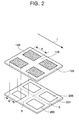
- FIG. 2 is a perspective view illustrating a donor substrate and an acceptor substrate according to an exemplary embodiment of the present invention
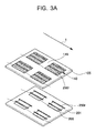
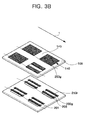
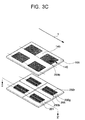
- FIGS. 3A through 3C are perspective views illustrating a method of fabricating an organic light emitting display (OLED) according to an exemplary embodiment of the present invention.
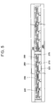
- FIGS. 4 and 5 are cross-sectional views illustrating a method of fabricating an OLED according to an exemplary embodiment of the present invention.
- FIG. 1 is a perspective view illustrating a method of fabricating a donor substrate according to an exemplary embodiment of the present invention.
- a light-to-heat conversion (LTHC) layer is formed on a base substrate 100 that has at least one transfer region and at least one non-transfer region.
- a transfer material is deposited on the LTHC layer in the transfer region using a shadow mask 50, thus forming a transfer layer.
- the base substrate 100 later becomes the donor substrate that is used to donate the patterned transfer layer to an acceptor substrate.
- the LTHC layer is made of a light absorption material that absorbs light in the infrared and visible regions.
- the LTHC layer is made of either an organic material, a metal, or a combination thereof.
- the LTHC layer contains a laser absorption material.
- the LTHC layer serves to convert laser beams irradiated by incident laser radiation into thermal energy. This thermal energy transforms adhesion between the transfer layer and the LTHC layer allowing the transfer layer to be transferred to an acceptor substrate.
- the shadow mask 50 is positioned over the base substrate 100 on which the LTHC layer is formed so that open regions 50a on shadow mask 50 correspond to the transfer regions. Then, the transfer layer is deposited onto base substrate 100 using the shadow mask 50.
- the transfer region is a region on base substrate 100 on which the transfer layer is formed and will be subsequently be transferred to an acceptor substrate through a laser induced thermal imaging (LITI) process.
- LITI laser induced thermal imaging
- a non-transfer region can be positioned between the two transfer regions.
- the transfer layer can be formed after a support plate 70 is fixed to the rear surface of the base substrate 100.
- the transfer layer can be an emission layer of an organic light emitting diode.
- the transfer layer can further include at least one of a hole injection layer, a hole transport layer, a hole blocking layer, and an electron injection layer.
- a buffer layer can be formed between the base substrate 100 and the LTHC layer or between the LTHC layer and the transfer layer in order to prevent damage to the transfer material and to reinforce adhesion between the transfer layer and the donor substrate.
- transfer material patterned in the transfer regions on the donor substrate is transferred via LITI to display regions on an acceptor substrate.
- the transfer regions on the donor substrate correspond to the display regions on the acceptor substrate.
- the width of the transfer layer formed in each of the transfer regions on the donor substrate can be designed to be slightly wider than a width of a corresponding display regions on the acceptor substrate. The difference in widths is used to compensate for either or both of alignment errors and edge effect errors.
- the dimension of an open region 50a of the shadow mask 50 is determined considering an alignment error that occur made when the transfer layer is transferred to the acceptor substrate.
- the dimension of the open region 50a is determined considering an edge effect, such that the transfer layer is transferred wider than the region that needs to be transferred by a thickness error of a pattern edge that can occur during the deposition of the transfer layer.
- the open region 50a of the shadow mask 50 can have a maximum value that adds the alignment error and a width for the edge effect to the pixel region.
- transfer material is formed only in places on the acceptor substrate where it is needed (i.e., the display regions) and not on portions of the acceptor substrate where the presence of transfer material is not needed and potentially harmful (i.e., the encapsulation portion).
- FIG. 2 is a view illustrating a donor substrate 105 and an acceptor substrate 201 according to an exemplary embodiment of the present invention. As illustrated in FIG. 2, the transfer layers 140 on the donor substrate 105 corresponds in pattern and location to the display regions 205 on the acceptor substrate 201.
- the donor substrate 105 which is fabricated as described with reference to FIG. 1, includes a transfer regions 140 and a non-transfer region 145, and a transfer layer is formed only on the transfer regions 140.
- the non-transfer region 145 can be located between the transfer regions 140.
- the patterned transfer layer can be made of an emission layer of an organic light emitting diode. Also, the patterned transfer layer can further include at least one of a hole injection layer, a hole transport layer, a hole blocking layer, and an electron injection layer.
- the donor substrate 105 is located over acceptor substrate 201.
- Acceptor substrate 201 includes at least one display region 205.
- a LITI process is carried out to transfer the transfer layers from the donor substrate 105 to the acceptor substrate 201 resulting in the transfer layers being formed in the display regions 205 on acceptor substrate 201.
- non-display region 203 located between the display regions 205 on acceptor substrate 201 does not need transfer material does not receive transfer material. This is accomplished without having to use on-off controlled lasers. In other words, even if laser beams are irradiated on the entire surface of the donor substrate 105, the transfer layer is patterned only on display regions 205 of acceptor substrate 201 where the transfer layers are needed.
- a patterned transfer layer is formed on the acceptor substrate without the use of either one of a mechanical shutter that operates at lower speed than the laser or a modulator that serves to control an on-off state of the laser. Accordingly, a failure in a pattern can be prevented, and the cost of production can be reduced.
- cleave lines 3 and 5 are also formed in non-display region 203 on acceptor substrate 201. After the completion of processing, the resultant can be cleaved into a plurality if OLEDs. Thus, the present process can be used to make a plurality of OLEDs simultaneously.
- Each of the transfer regions 140 on the donor substrate 105 is designed to be slightly wider than each of the corresponding display regions 205 on acceptor substrate 201 where the transfer material is to be transferred to.
- a difference between a width "a" of the transfer region 140 on donor substrate 105 and a width "b" of display region 205 on acceptor substrate is intentionally designed to compensate for alignment errors between the donor substrate 105 and the acceptor substrate 201 and also to compensate for thickness/edge effect errors of the transfer layer during the deposition of the transfer layer on the donor substrate 105.
- the maximum difference between the width "a" of the transfer region 140 on donor substrate 105 and the width "b" of the display region 205 on the acceptor substrate 201 can be obtained by adding an alignment error of a pixel region to edge effect errors.
- the transfer layer when the transfer layer is patterned on the acceptor substrate 201 using a donor substrate 105, a pattern failure caused by an alignment error can be compensated for and thus prevented. Also, a failure in edge thickness, which can be made when the transfer layer is formed on the donor substrate 105, does not take place even if the transfer layer is transferred to the acceptor substrate 201. Consequently, the transfer layer can be patterned more effectively on the acceptor substrate 201.
- FIGS. 3A through 3C are perspective views illustrating a method of fabricating an OLED according to an exemplary embodiment of the present invention.
- the OLED is fabricated using the above-described donor substrate.
- FIGS. 3A through 3C describe a process where the transfer layer is patterned in the order of the R, G, and B unit pixel regions, it is to be appreciated that other color orders can occur and still be within the scope of the present invention.
- a donor substrate 105 including transfer regions 140 and a non-transfer region 145 is prepared.
- a transfer layer is patterned within the transfer regions 140.
- the non-transfer region 145 can be located between the two transfer regions 140.
- the donor substrate 105 can be larger than the acceptor substrate 201.
- the donor substrate 105 can further include a buffer layer interposed between the transfer layer and an LTHC layer or between the base substrate and the LTHC layer.
- the acceptor substrate 201 includes at least one display region 205, each display region 205 being aligned and opposite to corresponding transfer regions 140 formed on donor substrate 105.
- the transfers regions 140 can contain transfer layers that can include an emission layer.
- the transfer layer can further include at least one of a hole injection layer, a hole transport layer, a hole blocking layer, and an electron injection layer.
- the donor substrate 105 includes at least one transfer region 140 and a non-transfer region 145, and an R transfer layer 250r made of an R (red) emission material is selectively formed on the transfer region 140 using a shadow mask.
- the donor substrate 105 on which the R emission layer 250r is formed is aligned with and located over the display region 205 of acceptor substrate 201. Thereafter, the patterned R emission layer 250r is transferred onto the display region 205 of the substrate 201 via a LITI process.
- the transfer layer 250r can be transferred onto the display region 205 of acceptor substrate 201 by irradiating continuous-wave (CW) laser beams 1 onto the donor substrate 105. As a result, the R emission layer 250r is formed in an R unit pixel regions in display region 205 on the acceptor substrate 201.
- CW continuous-wave
- a G emission layer 250g is transferred to G unit pixel region on the display region 205 on acceptor substrate 201 on which the R emission layer 250r is formed, in the same manner as described with reference to FIG. 3A.
- a B (blue) emission layer 250b is transferred to a B unit pixel region on the display region 205 of acceptor substrate 201 using the donor substrate 105 on which a B emission layer is patterned, in the same manner as described with reference to FIGS. 3A and 3B.
- the occurrence of transferring emission material to portions of the acceptor substrate that do not need the transfer layer, such as the encapsulation portion, can be avoided.
- a process of removing emission material from portions of the acceptor substrate outside of the display regions can be avoided.
- laser irradiation is continuously performed, it is unnecessary to adopt an on-off controller for discontinuous laser irradiation to pattern the transfer layer. Accordingly, the cost of production is reduced. Further, an organic layer is not present in the encapsulation portion so that deterioration of the adhesive properties of the sealant applied can be avoided.
- the patterned emission layers 250r, 250g, and 250b are formed to be slightly larger than the display regions 205.
- the patterned region of the emission layer i.e., the transfer region 140 on the donor substrate 105 can be formed wider than the display region 205 on acceptor substrate 201 to compensate for alignment errors.
- a pattern failure caused by an alignment error between the donor substrate 105 and the acceptor substrate 201 can be prevented.
- the transfer region 140 of the donor substrate 105 can further be formed wider than the display region 205 on acceptor substrate 201 to compensate for an edge effect. As a result, failures in edge thickness that can occur when the transfer layer is formed on the donor substrate 105, does not occur even when the transfer layer is transferred on the acceptor substrate 201 because of the compensation. As a result, the transfer layer can be patterned more effectively.
- FIGS. 4 and 5 are the cross sectional views are taken along line II-II' of FIG. 3C illustrating a method of fabricating an OLED using the above-described donor substrate according to an exemplary embodiment of the present invention.
- FIG. 3C shows the presence of three colors of emission material formed within each display region on acceptor substrate, FIGS. 4 and 5 instead correspond to unit pixels in any one color.
- a predetermined layer including thin film transistors (TFTs) 210 is formed on a lower substrate 200 in at least one display region "b". Specifically, a gate electrode, a source electrode, and a drain electrode are formed on the lower substrate 200. In addition to the TFTs 210, a capacitor or metal interconnections are formed. An insulating layer 220 is formed on the resultant structure. Insulating layer 220 can include a gate insulating layer and an interlayer insulating layer. Insulating layer can further include a passivation layer or a planarization layer. Thus, the TFTs 210 and the insulating layer 220 are formed in each of the unit pixel regions of the lower substrate 200.
- TFTs thin film transistors
- Pixel electrodes 230 are formed so that they are connected to the TFTs 210.
- a reflection layer can be interposed between the pixel electrodes 230 and the insulating layer 220.
- a pixel defining layer 240 is formed on the pixel electrodes 230 on the lower substrate 200 to define each of the unit pixel regions.
- An emission layer 250 is formed on the pixel defining layer 240 using the donor substrate in the same manner as described above.
- the emission layer is not transferred to encapsulation portions "A" where the presence of emission material is not needed and can be harmful.
- a region "a" of the patterned emission layer 250 is formed wider than a display region "b” to compensate for alignment and edge thickness errors. As a result, the emission layer 250 can be patterned more effectively.
- an opposite electrode 260 is formed on the lower substrate 200 on which the emission layer 250 is formed. Thereafter, a sealant 270 is formed on every encapsulation portion "A" between the display regions "b". The resultant structure is then encapsulated using an upper substrate 280, and the encapsulated structure is severed into respective display devices. As a result, the formation of one or more OLEDs is completed.
- a transfer layer on a donor substrate is patterned and formed only in a transfer region.
- a process of removing transfer material from regions outside of the transfer region because no organic material is formed in the encapsulation portion, deterioration of adhesive properties of sealant applied in the encapsulation portion can be avoided.
- a pattern can be formed only in a display region during an LITI process without using any additional on-off controller for a laser.
- the patterned transfer layer on the donor substrate is formed to be slightly wider than the display region of the OLED. Accordingly, a pattern failure caused by an alignment error between the donor substrate and the acceptor substrate can be prevented, and a failure in edge thickness, which can be made when the transfer layer is formed on the donor substrate, can also be prevented even when the transfer layer is transferred to the acceptor substrate. As a result, the transfer layer can be patterned more effectively.
Landscapes
- Physics & Mathematics (AREA)
- Optics & Photonics (AREA)
- Engineering & Computer Science (AREA)
- Manufacturing & Machinery (AREA)
- Electroluminescent Light Sources (AREA)
Applications Claiming Priority (1)
| Application Number | Priority Date | Filing Date | Title |
|---|---|---|---|
| KR1020040079250A KR100793355B1 (ko) | 2004-10-05 | 2004-10-05 | 도너 기판의 제조방법 및 유기전계발광표시장치의 제조방법 |
Publications (2)
| Publication Number | Publication Date |
|---|---|
| EP1646094A1 true EP1646094A1 (fr) | 2006-04-12 |
| EP1646094B1 EP1646094B1 (fr) | 2009-04-08 |
Family
ID=36125940
Family Applications (1)
| Application Number | Title | Priority Date | Filing Date |
|---|---|---|---|
| EP05109172A Expired - Lifetime EP1646094B1 (fr) | 2004-10-05 | 2005-10-04 | Procédé de fabrication d'un OLED au moyen du substrat donneur |
Country Status (6)
| Country | Link |
|---|---|
| US (1) | US7223514B2 (fr) |
| EP (1) | EP1646094B1 (fr) |
| JP (1) | JP4535387B2 (fr) |
| KR (1) | KR100793355B1 (fr) |
| CN (1) | CN100388422C (fr) |
| DE (1) | DE602005013729D1 (fr) |
Cited By (2)
| Publication number | Priority date | Publication date | Assignee | Title |
|---|---|---|---|---|
| US8581234B2 (en) | 2008-02-29 | 2013-11-12 | Semiconductor Energy Laboratory Co., Ltd. | Deposition method and manufacturing method of light-emitting device |
| EP3287291A1 (fr) * | 2016-08-26 | 2018-02-28 | Nederlandse Organisatie voor toegepast- natuurwetenschappelijk onderzoek TNO | Procédé et système d'application d'une structure à motifs sur une surface |
Families Citing this family (16)
| Publication number | Priority date | Publication date | Assignee | Title |
|---|---|---|---|---|
| KR100769431B1 (ko) * | 2006-06-09 | 2007-10-22 | 삼성에스디아이 주식회사 | 도너필름의 제조방법 및 이를 이용한 유기 전계발광표시장치의 제조방법 |
| US7419757B2 (en) * | 2006-10-20 | 2008-09-02 | 3M Innovative Properties Company | Structured thermal transfer donors |
| JP2008235010A (ja) * | 2007-03-20 | 2008-10-02 | Sony Corp | 表示装置の製造方法 |
| CN101271869B (zh) * | 2007-03-22 | 2015-11-25 | 株式会社半导体能源研究所 | 发光器件的制造方法 |
| US20090130427A1 (en) * | 2007-10-22 | 2009-05-21 | The Regents Of The University Of California | Nanomaterial facilitated laser transfer |
| US8425974B2 (en) * | 2007-11-29 | 2013-04-23 | Semiconductor Energy Laboratory Co., Ltd. | Evaporation donor substrate and method for manufacturing light-emitting device |
| US8080811B2 (en) | 2007-12-28 | 2011-12-20 | Semiconductor Energy Laboratory Co., Ltd. | Method for manufacturing evaporation donor substrate and light-emitting device |
| US8182863B2 (en) * | 2008-03-17 | 2012-05-22 | Semiconductor Energy Laboratory Co., Ltd. | Deposition method and manufacturing method of light-emitting device |
| US7932112B2 (en) * | 2008-04-14 | 2011-04-26 | Semiconductor Energy Laboratory Co., Ltd. | Method for manufacturing light-emitting device |
| KR101629637B1 (ko) * | 2008-05-29 | 2016-06-13 | 가부시키가이샤 한도오따이 에네루기 켄큐쇼 | 성막방법 및 발광장치의 제조방법 |
| KR101084179B1 (ko) * | 2009-12-28 | 2011-11-17 | 삼성모바일디스플레이주식회사 | 유기 발광 디스플레이 소자의 봉지 방법 |
| KR20130010628A (ko) * | 2011-07-19 | 2013-01-29 | 삼성디스플레이 주식회사 | 도너 기판, 도너 기판의 제조 방법 및 도너 기판을 이용한 유기 발광 표시 장치의 제조 방법 |
| CN103882374B (zh) | 2014-03-03 | 2016-01-13 | 京东方科技集团股份有限公司 | 掩膜版、有机层加工方法、显示基板制备方法 |
| CN105870265A (zh) | 2016-04-19 | 2016-08-17 | 京东方科技集团股份有限公司 | 发光二极管基板及其制备方法、显示装置 |
| CN108598132A (zh) | 2018-05-23 | 2018-09-28 | 京东方科技集团股份有限公司 | 显示基板的制作方法、掩膜板的制作方法、显示装置 |
| CN111254385A (zh) * | 2020-01-19 | 2020-06-09 | 阿德文泰克全球有限公司 | 金属荫罩及其制备方法,电铸模板及其制备方法 |
Citations (5)
| Publication number | Priority date | Publication date | Assignee | Title |
|---|---|---|---|---|
| EP0773707A2 (fr) | 1995-11-13 | 1997-05-14 | Eastman Kodak Company | Procédé pour la fabrication d'un panneau d'affichage électroluminescent en matière organique |
| EP0913870A2 (fr) * | 1997-10-31 | 1999-05-06 | Eastman Kodak Company | Méthode de transfert sélectif d'une couche organique colorée |
| US6403392B1 (en) * | 1998-10-30 | 2002-06-11 | The Trustees Of Princeton University | Method for patterning devices |
| WO2002070271A2 (fr) * | 2001-03-01 | 2002-09-12 | E. I. Du Pont De Nemours And Company | Procedes d'imagerie thermique et produits de materiau organique electroactif |
| US20050112303A1 (en) * | 2003-11-25 | 2005-05-26 | Mu-Hyun Kim | Donor substrate for full-color organic electroluminescent display device, method of manufacturing the same, and full-color organic electroluminescent display device using donor substrate |
Family Cites Families (16)
| Publication number | Priority date | Publication date | Assignee | Title |
|---|---|---|---|---|
| US5863860A (en) * | 1995-01-26 | 1999-01-26 | Minnesota Mining And Manufacturing Company | Thermal transfer imaging |
| KR100441522B1 (ko) * | 1996-10-23 | 2004-10-14 | 삼성에스디아이 주식회사 | 미소형상 형성용 전사필름 및 그 장치 |
| KR100195175B1 (ko) * | 1996-12-23 | 1999-06-15 | 손욱 | 유기전자발광소자 유기박막용 도너필름, 이를 이용한 유기전자발광소자의 제조방법 및 그 방법에 따라 제조된 유기전자발광소자 |
| US5937272A (en) * | 1997-06-06 | 1999-08-10 | Eastman Kodak Company | Patterned organic layers in a full-color organic electroluminescent display array on a thin film transistor array substrate |
| JP2000195665A (ja) * | 1998-12-25 | 2000-07-14 | Toyota Motor Corp | 有機膜の形成方法 |
| US6114088A (en) * | 1999-01-15 | 2000-09-05 | 3M Innovative Properties Company | Thermal transfer element for forming multilayer devices |
| JP4590663B2 (ja) * | 1999-10-29 | 2010-12-01 | セイコーエプソン株式会社 | カラーフィルタの製造方法 |
| TW501379B (en) * | 2000-07-25 | 2002-09-01 | Eastman Kodak Co | Method of making organic electroluminescent device using laser transfer |
| KR100741052B1 (ko) | 2000-10-16 | 2007-07-19 | 삼성에스디아이 주식회사 | 유기 el 소자의 증착마스크와 이를 이용한 증착방법 및그 장치 |
| US6485884B2 (en) * | 2001-04-27 | 2002-11-26 | 3M Innovative Properties Company | Method for patterning oriented materials for organic electronic displays and devices |
| JP2003031359A (ja) * | 2001-07-10 | 2003-01-31 | Sharp Corp | 薄膜製造装置およびそれを用いて製造された有機エレクトロルミネッセンス素子 |
| US6695029B2 (en) * | 2001-12-12 | 2004-02-24 | Eastman Kodak Company | Apparatus for permitting transfer of organic material from a donor to form a layer in an OLED device |
| JP2003347054A (ja) * | 2002-05-29 | 2003-12-05 | Sharp Corp | 薄膜転写用フィルムとその製造方法およびそれを用いた有機el素子 |
| US6682863B2 (en) * | 2002-06-27 | 2004-01-27 | Eastman Kodak Company | Depositing an emissive layer for use in an organic light-emitting display device (OLED) |
| US6890627B2 (en) * | 2002-08-02 | 2005-05-10 | Eastman Kodak Company | Laser thermal transfer from a donor element containing a hole-transporting layer |
| KR100501315B1 (ko) * | 2002-12-17 | 2005-07-18 | 삼성에스디아이 주식회사 | 레이저 전사법을 사용하는 저분자 풀칼라 유기 전계 발광소자용 도너 필름 및 그 필름을 사용하는 저분자 풀칼라유기 전계 발광 소자의 제조 방법 |
-
2004
- 2004-10-05 KR KR1020040079250A patent/KR100793355B1/ko not_active Expired - Fee Related
-
2005
- 2005-09-28 US US11/236,494 patent/US7223514B2/en not_active Expired - Fee Related
- 2005-10-03 JP JP2005289898A patent/JP4535387B2/ja not_active Expired - Fee Related
- 2005-10-04 EP EP05109172A patent/EP1646094B1/fr not_active Expired - Lifetime
- 2005-10-04 DE DE602005013729T patent/DE602005013729D1/de not_active Expired - Lifetime
- 2005-10-08 CN CNB2005101291433A patent/CN100388422C/zh not_active Expired - Fee Related
Patent Citations (5)
| Publication number | Priority date | Publication date | Assignee | Title |
|---|---|---|---|---|
| EP0773707A2 (fr) | 1995-11-13 | 1997-05-14 | Eastman Kodak Company | Procédé pour la fabrication d'un panneau d'affichage électroluminescent en matière organique |
| EP0913870A2 (fr) * | 1997-10-31 | 1999-05-06 | Eastman Kodak Company | Méthode de transfert sélectif d'une couche organique colorée |
| US6403392B1 (en) * | 1998-10-30 | 2002-06-11 | The Trustees Of Princeton University | Method for patterning devices |
| WO2002070271A2 (fr) * | 2001-03-01 | 2002-09-12 | E. I. Du Pont De Nemours And Company | Procedes d'imagerie thermique et produits de materiau organique electroactif |
| US20050112303A1 (en) * | 2003-11-25 | 2005-05-26 | Mu-Hyun Kim | Donor substrate for full-color organic electroluminescent display device, method of manufacturing the same, and full-color organic electroluminescent display device using donor substrate |
Cited By (5)
| Publication number | Priority date | Publication date | Assignee | Title |
|---|---|---|---|---|
| US8581234B2 (en) | 2008-02-29 | 2013-11-12 | Semiconductor Energy Laboratory Co., Ltd. | Deposition method and manufacturing method of light-emitting device |
| EP3287291A1 (fr) * | 2016-08-26 | 2018-02-28 | Nederlandse Organisatie voor toegepast- natuurwetenschappelijk onderzoek TNO | Procédé et système d'application d'une structure à motifs sur une surface |
| WO2018038613A1 (fr) * | 2016-08-26 | 2018-03-01 | Nederlandse Organisatie Voor Toegepast-Natuurwetenschappelijk Onderzoek Tno | Procédé et système permettant d'appliquer une structure à motifs sur une surface |
| KR20190039794A (ko) * | 2016-08-26 | 2019-04-15 | 네덜란제 오르가니자티에 포오르 토에게파스트-나투우르베텐샤펠리즈크 온데르조에크 테엔오 | 표면에 패터닝된 구조를 적용하기 위한 방법 및 시스템 |
| US11173737B2 (en) | 2016-08-26 | 2021-11-16 | Nederlandse Organisatie Voor Toegepast-Natuurwetenschappelijk Onderzoek Tno | Method and system for applying a patterned structure on a surface |
Also Published As
| Publication number | Publication date |
|---|---|
| EP1646094B1 (fr) | 2009-04-08 |
| US7223514B2 (en) | 2007-05-29 |
| US20060073406A1 (en) | 2006-04-06 |
| KR20060030405A (ko) | 2006-04-10 |
| JP2006108098A (ja) | 2006-04-20 |
| DE602005013729D1 (de) | 2009-05-20 |
| CN100388422C (zh) | 2008-05-14 |
| KR100793355B1 (ko) | 2008-01-11 |
| CN1797713A (zh) | 2006-07-05 |
| JP4535387B2 (ja) | 2010-09-01 |
Similar Documents
| Publication | Publication Date | Title |
|---|---|---|
| EP1646094B1 (fr) | Procédé de fabrication d'un OLED au moyen du substrat donneur | |
| US7247986B2 (en) | Organic electro luminescent display and method for fabricating the same | |
| EP2251906B1 (fr) | Procédé de fabrication d'affichage à diode électroluminescente organique | |
| US7674749B2 (en) | Donor substrate and fabrication method of organic light emitting display using the same | |
| US7612498B2 (en) | Display element, optical device, and optical device manufacturing method | |
| US20070046185A1 (en) | Organic light emitting display and method for fabricating the same | |
| KR20140123787A (ko) | 유기 발광 표시 장치 및 그 제조 방법 | |
| CN104576957A (zh) | 有机电致发光显示设备及其制造方法 | |
| KR100477565B1 (ko) | 평면표시장치용 어레이 기판의 제조방법 및평면표시장치의 제조방법 | |
| US7867846B2 (en) | Organic light emitting display (OLED) having a gas vent groove to decrease edge open failures | |
| EP1826738A1 (fr) | Dispositif d'affichage et procede de fabrication du dispositif d'affichage | |
| US7686052B2 (en) | Lamination apparatus and laser-induced thermal imaging method using the same | |
| US7635609B2 (en) | Patterning method for light-emitting devices | |
| JP2006004743A (ja) | 表示装置及びその製造方法 | |
| US8004184B2 (en) | Electro-luminescent display device | |
| JP5215804B2 (ja) | 有機el表示装置の製造方法 | |
| KR100592280B1 (ko) | 평판 표시장치의 제조방법, 및 평판 표시장치 | |
| KR20140140870A (ko) | 유기발광 표시패널 제조방법 | |
| KR20050111493A (ko) | 평판 표시 장치 및 그 제조방법 | |
| KR20070115339A (ko) | 레이저 열 전사 장치 및 이를 이용한 유기 발광소자의제조방법 |
Legal Events
| Date | Code | Title | Description |
|---|---|---|---|
| PUAI | Public reference made under article 153(3) epc to a published international application that has entered the european phase |
Free format text: ORIGINAL CODE: 0009012 |
|
| AK | Designated contracting states |
Kind code of ref document: A1 Designated state(s): AT BE BG CH CY CZ DE DK EE ES FI FR GB GR HU IE IS IT LI LT LU LV MC NL PL PT RO SE SI SK TR |
|
| AX | Request for extension of the european patent |
Extension state: AL BA HR MK YU |
|
| 17P | Request for examination filed |
Effective date: 20060802 |
|
| 17Q | First examination report despatched |
Effective date: 20060906 |
|
| AKX | Designation fees paid |
Designated state(s): DE FR GB NL |
|
| 17Q | First examination report despatched |
Effective date: 20060906 |
|
| GRAP | Despatch of communication of intention to grant a patent |
Free format text: ORIGINAL CODE: EPIDOSNIGR1 |
|
| RIC1 | Information provided on ipc code assigned before grant |
Ipc: H01L 51/00 20060101AFI20081031BHEP |
|
| RTI1 | Title (correction) |
Free format text: METHOD OF FABRICATING AN OLED USING A DONOR SUBSTRATE |
|
| RAP1 | Party data changed (applicant data changed or rights of an application transferred) |
Owner name: SAMSUNG MOBILE DISPLAY CO., LTD. |
|
| GRAS | Grant fee paid |
Free format text: ORIGINAL CODE: EPIDOSNIGR3 |
|
| GRAA | (expected) grant |
Free format text: ORIGINAL CODE: 0009210 |
|
| AK | Designated contracting states |
Kind code of ref document: B1 Designated state(s): DE FR GB NL |
|
| REG | Reference to a national code |
Ref country code: GB Ref legal event code: FG4D |
|
| REF | Corresponds to: |
Ref document number: 602005013729 Country of ref document: DE Date of ref document: 20090520 Kind code of ref document: P |
|
| PLBE | No opposition filed within time limit |
Free format text: ORIGINAL CODE: 0009261 |
|
| STAA | Information on the status of an ep patent application or granted ep patent |
Free format text: STATUS: NO OPPOSITION FILED WITHIN TIME LIMIT |
|
| PGFP | Annual fee paid to national office [announced via postgrant information from national office to epo] |
Ref country code: NL Payment date: 20091004 Year of fee payment: 5 |
|
| 26N | No opposition filed |
Effective date: 20100111 |
|
| REG | Reference to a national code |
Ref country code: NL Ref legal event code: V1 Effective date: 20110501 |
|
| PG25 | Lapsed in a contracting state [announced via postgrant information from national office to epo] |
Ref country code: NL Free format text: LAPSE BECAUSE OF NON-PAYMENT OF DUE FEES Effective date: 20110501 |
|
| REG | Reference to a national code |
Ref country code: DE Ref legal event code: R082 Ref document number: 602005013729 Country of ref document: DE Representative=s name: GULDE HENGELHAUPT ZIEBIG & SCHNEIDER, DE |
|
| REG | Reference to a national code |
Ref country code: DE Ref legal event code: R082 Ref document number: 602005013729 Country of ref document: DE Representative=s name: GULDE HENGELHAUPT ZIEBIG & SCHNEIDER, DE Effective date: 20121026 Ref country code: DE Ref legal event code: R081 Ref document number: 602005013729 Country of ref document: DE Owner name: SAMSUNG DISPLAY CO., LTD., KR Free format text: FORMER OWNER: SAMSUNG MOBILE DISPLAY CO. LTD., SUWON, KR Effective date: 20121026 Ref country code: DE Ref legal event code: R081 Ref document number: 602005013729 Country of ref document: DE Owner name: SAMSUNG DISPLAY CO., LTD., YONGIN-CITY, KR Free format text: FORMER OWNER: SAMSUNG MOBILE DISPLAY CO. LTD., SUWON, GYEONGGI, KR Effective date: 20121026 Ref country code: DE Ref legal event code: R082 Ref document number: 602005013729 Country of ref document: DE Representative=s name: GULDE & PARTNER PATENT- UND RECHTSANWALTSKANZL, DE Effective date: 20121026 |
|
| REG | Reference to a national code |
Ref country code: GB Ref legal event code: 732E Free format text: REGISTERED BETWEEN 20130110 AND 20130116 |
|
| REG | Reference to a national code |
Ref country code: FR Ref legal event code: TP Owner name: SAMSUNG DISPLAY CO., LTD., KR Effective date: 20130130 |
|
| REG | Reference to a national code |
Ref country code: FR Ref legal event code: PLFP Year of fee payment: 11 |
|
| PGFP | Annual fee paid to national office [announced via postgrant information from national office to epo] |
Ref country code: GB Payment date: 20151009 Year of fee payment: 11 Ref country code: DE Payment date: 20151019 Year of fee payment: 11 |
|
| PGFP | Annual fee paid to national office [announced via postgrant information from national office to epo] |
Ref country code: FR Payment date: 20151026 Year of fee payment: 11 |
|
| REG | Reference to a national code |
Ref country code: DE Ref legal event code: R119 Ref document number: 602005013729 Country of ref document: DE |
|
| GBPC | Gb: european patent ceased through non-payment of renewal fee |
Effective date: 20161004 |
|
| REG | Reference to a national code |
Ref country code: FR Ref legal event code: ST Effective date: 20170630 |
|
| PG25 | Lapsed in a contracting state [announced via postgrant information from national office to epo] |
Ref country code: FR Free format text: LAPSE BECAUSE OF NON-PAYMENT OF DUE FEES Effective date: 20161102 Ref country code: GB Free format text: LAPSE BECAUSE OF NON-PAYMENT OF DUE FEES Effective date: 20161004 Ref country code: DE Free format text: LAPSE BECAUSE OF NON-PAYMENT OF DUE FEES Effective date: 20170503 |