EP0913870A2 - Méthode de transfert sélectif d'une couche organique colorée - Google Patents
Méthode de transfert sélectif d'une couche organique colorée Download PDFInfo
- Publication number
- EP0913870A2 EP0913870A2 EP98203510A EP98203510A EP0913870A2 EP 0913870 A2 EP0913870 A2 EP 0913870A2 EP 98203510 A EP98203510 A EP 98203510A EP 98203510 A EP98203510 A EP 98203510A EP 0913870 A2 EP0913870 A2 EP 0913870A2
- Authority
- EP
- European Patent Office
- Prior art keywords
- layer
- color
- openings
- substrate
- organic
- Prior art date
- Legal status (The legal status is an assumption and is not a legal conclusion. Google has not performed a legal analysis and makes no representation as to the accuracy of the status listed.)
- Withdrawn
Links
Images
Classifications
-
- B—PERFORMING OPERATIONS; TRANSPORTING
- B41—PRINTING; LINING MACHINES; TYPEWRITERS; STAMPS
- B41M—PRINTING, DUPLICATING, MARKING, OR COPYING PROCESSES; COLOUR PRINTING
- B41M5/00—Duplicating or marking methods; Sheet materials for use therein
- B41M5/26—Thermography ; Marking by high energetic means, e.g. laser otherwise than by burning, and characterised by the material used
- B41M5/382—Contact thermal transfer or sublimation processes
- B41M5/38207—Contact thermal transfer or sublimation processes characterised by aspects not provided for in groups B41M5/385 - B41M5/395
- B41M5/38214—Structural details, e.g. multilayer systems
-
- G—PHYSICS
- G02—OPTICS
- G02B—OPTICAL ELEMENTS, SYSTEMS OR APPARATUS
- G02B5/00—Optical elements other than lenses
- G02B5/20—Filters
- G02B5/201—Filters in the form of arrays
-
- H—ELECTRICITY
- H10—SEMICONDUCTOR DEVICES; ELECTRIC SOLID-STATE DEVICES NOT OTHERWISE PROVIDED FOR
- H10F—INORGANIC SEMICONDUCTOR DEVICES SENSITIVE TO INFRARED RADIATION, LIGHT, ELECTROMAGNETIC RADIATION OF SHORTER WAVELENGTH OR CORPUSCULAR RADIATION
- H10F77/00—Constructional details of devices covered by this subclass
- H10F77/30—Coatings
- H10F77/306—Coatings for devices having potential barriers
- H10F77/331—Coatings for devices having potential barriers for filtering or shielding light, e.g. multicolour filters for photodetectors
-
- H—ELECTRICITY
- H10—SEMICONDUCTOR DEVICES; ELECTRIC SOLID-STATE DEVICES NOT OTHERWISE PROVIDED FOR
- H10K—ORGANIC ELECTRIC SOLID-STATE DEVICES
- H10K71/00—Manufacture or treatment specially adapted for the organic devices covered by this subclass
- H10K71/10—Deposition of organic active material
- H10K71/18—Deposition of organic active material using non-liquid printing techniques, e.g. thermal transfer printing from a donor sheet
-
- H—ELECTRICITY
- H10—SEMICONDUCTOR DEVICES; ELECTRIC SOLID-STATE DEVICES NOT OTHERWISE PROVIDED FOR
- H10K—ORGANIC ELECTRIC SOLID-STATE DEVICES
- H10K59/00—Integrated devices, or assemblies of multiple devices, comprising at least one organic light-emitting element covered by group H10K50/00
- H10K59/30—Devices specially adapted for multicolour light emission
- H10K59/35—Devices specially adapted for multicolour light emission comprising red-green-blue [RGB] subpixels
-
- H—ELECTRICITY
- H10—SEMICONDUCTOR DEVICES; ELECTRIC SOLID-STATE DEVICES NOT OTHERWISE PROVIDED FOR
- H10K—ORGANIC ELECTRIC SOLID-STATE DEVICES
- H10K71/00—Manufacture or treatment specially adapted for the organic devices covered by this subclass
Definitions
- the present invention relates to methods for selective transfer of a color organic layer from a transferrable color forming organic donor layer to a device having designated red, green, and blue color subpixels.
- color forming media for example red, green, and blue color forming media
- the color forming media are deposited so as to provide a color filter over the pixels.
- the solid-state image sensing device can be a charge coupled device (CCD) or a complementary metal oxide semiconductor (CMOS) device.
- CMOS complementary metal oxide semiconductor
- a full color light emitting electroluminescent (EL) device red, green, or blue color light emitting pixels or subpixels are formed by pixel-selective deposition of red, green, or blue light emitting organic EL media.
- each color forming EL-medium is comprised of a thin layer of an organic EL host material and, respectively, a red, green, or blue light emitting fluorescent dye.
- Such layers are neat layers, that is, the layers do not contain polymeric binders, and the layers have a thickness in the range of from 200 to 1000 Angstrom.
- Organic color filter arrays on image sensing devices are currently provided by photolithographic patterning of a predeposited uniform layer of a photolithographic composition which either contains a selected colorant, or into which a colorant can be introduced upon patterning.
- lithographically patternable color filter layers contain a photopolymer material, and have a typical thickness in the range of from 10,000 to 20,000 Angstrom.
- This object is achieved by a method for selective transfer of a color organic layer from a donor layer onto a device having an array of pixels with each pixel formed from a number of color subpixels having seleced positions in the array, comprising the steps of:
- the present invention provides selective transfer to a device from a color forming organic donor layer bearing structure upon exposure to radiation.
- the invention employs regions of high radiation absorbance, low thermal mass, and low thermal conductivity where efficient transfer of the color forming organic donor layer to the device is desired, and having regions of high thermal mass, and high thermal conductivity from which transfer of a color forming organic layer is precluded.
- Major advantages include high pixel resolution and edge definition of transferred layers; excellent utilization of the color forming organic donor layer; precise control of the thickness of each selectively transferred color forming organic layer; in scalability to large area device; and compact deposition tooling.
- the term "display” is employed to designate a screen capable of electronically displaying video images or text.
- pixel is employed in its art recognized usage to designate an area of a display that can be stimulated to emit light independently of other areas.
- full color is employed to describe a display which is capable of rendering video images or text in the red, green, and blue regions of the visible spectrum and displaying images in any combination of hues.
- the red, green, and blue colors constitute the three primary colors from which all other colors can be generated by appropriately mixing these three primaries.
- the term “hue” refers to the intensity profile of light within the visible spectrum, with different hues exhibiting visually discernible differences in color.
- the pixel or subpixel is generally used to designate the smallest addressable unit in a display.
- subpixel is employed to designate any portion of a pixel which can be independently addressable to render a specific color.
- a blue subpixel is that portion of a pixel which can be addressed to provide blue light.
- a pixel In a full color display, a pixel generally comprises three primary color subpixels, namely, blue, green, and red.
- the term "pitch" is used to designate the distance separating two pixels or two subpixels. Thus, a subpixel pitch means the separation between two subpixels.
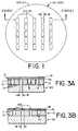
- FIG. 1 there is shown a schematic plan view of a silicon wafer substrate 10 as viewed from a second surface 12.
- the substrate 10 has an ordered array of a plurality of openings 14 with each opening having a width dimension W.
- the width dimension W of the openings can be in a range of from about 1 to about 500 micrometer, and is preferably in a range of from 2 to 300 micrometer commensurate with a range of pixel width dimensions of various classes of image sensing device and of various designs of EL display devices.
- a line 2B-2B indicates a cross-sectional view of a FIG. 2B, and designations shown in parentheses in FIG. 1 refer to a second embodiment of the method and methods in accordance with the present invention and to be detailed with reference to FIGS. 4A-4D.
- a silicon wafer is one preferred substrate for the method of the present invention for the following major reasons: silicon wafers and silicon wafer processing equipment are readily commercially available; recent advances in silicon wafer processing have provided suitable methods in forming deep openings or deep trenches in a silicon wafer by combining standard photolithography with techniques of high density plasma etching as described, for example, in a publication by J.K. Bhardwaj and H. Ashraf, titled “Advanced Silicon Etching Using High Density Plasmas," SPIE: Micromachining and Microfabrication Process Technology, Vol.
- silicon wafers exhibit substantial structural integrity and thermal stability under operating conditions experienced by the silicon wafer substrate when used in the apparatus of the present invention; and the two opposing surfaces of a silicon wafer substrate are substantially coplanar and polished, thus permitting deposition of well defined thin films thereon.
- the microfabrication method can be readily extended to other substrates such as glass and ceramic plates or wafers.
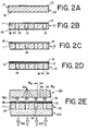
- FIG. 2A there is provided a schematic cross-sectional view of a substrate 10 having a first surface 11 and an opposing second surface 12 with a light transmissive and thermally insulating layer 13 deposited on the first surface 11 of the substrate.
- the layer 13 should have a low thermal conductivity, or it should be sufficiently thin such that its total thermal mass is small compared with the thermal mass of the wafer substrate.
- Particularly preferred materials forming layer 13 are silicon dioxide, silicon nitride, silicon oxynitride, and aluminum oxide.
- the thickness of this layer is preferably in the range of from 0.1 to 50 micrometer.
- FIG. 2B there is shown a schematic cross-sectional view of the substrate 10 taken along the lines 2B-2B of FIG. 1, depicting periodically spaced openings 14 extending from the second surface 12 to the first surface 11 of the substrate.
- the openings 14 have a width dimension W, and are formed by the aforementioned high density plasma etching process in which the insulating layer 13 serves as an etch stop for the etch process which is initiated from the second surface 12.
- the openings 14 are arranged in a pattern which is common with the pattern of the subpixels of a device upon which a color forming organic layer is to be selectively transferred.
- the width dimension W of the openings 14 is preferably in a range of from 2 to 300 micrometer.
- a light absorbing layer 15 is shown disposed on the insulating layer 13.
- an average absorbance of the light absorbing layer should have a value of at least 1.0 over the spectral wavelength range of the radiation source.
- the physical thickness of the light absorbing layer 15 can be in a range from about 0.1 micrometer to several micrometers. Any absorptive materials compatible with the processing of a silicon wafer substrate are useful.
- Preferred materials for the light absorbing layer include single layers of chromium, nickel, cobalt, silicon, germanium, and carbon, or alloys of these materials.
- a multilayer stack of alternating layers of materials for example of alternating layers of chromium and germanium, can be used to desirably match the absorptive range of the light absorbing layer to the spectral characteristics of the radiation source, and to reduce generally undesirable reflective characteristics of the light absorbing layer.
- the substrate, the heat insulating layer, and the light absorbing layer must be durable and preferably useful in multiple processing cycle. Therefore, it is important that the light absorbing layer 15 has high thermal stability, good adhesion to the insulating layer 13, and abrasion resistance to withstand the thermal transfer cycles and any subsequent cleaning processes following each transfer process. Cleaning processes include solvent cleaning, ultrasonic solvent cleaning, gas plasma treatment, scrubbing, and thermal deposition at high temperatures.
- FIG. 2D there is shown disposed on the light absorbing layer 15, layer 16 of a color forming organic material.
- This color forming organic material is necessarily a sublimable neat layer and forms a continuous and uniform film upon transfer using the method of the present invention.
- the desirable characteristics are thermal and photochemical stability, high glass transition temperature, and an organic EL-medium comprised of one or more light-emissive organic materials.
- the color forming organic donor layer 16 is deposited on the light absorbing layer 15 to a thickness in the range of from 0.1 to 10 micrometer, preferably by vapor deposition methods.
- color forming colorants which are useful as a donor layer for selective transfer onto an image sensing device to form a color filter thereon include the following: phthalocyanines, such as Pigment Blue 15, nickel phthalocyanine, chloroaluminum phthalocyanine, hydroxy aluminum phthalocyanine, vanadyl phthalocyanine, titanyl phthalocyanine, and titanyl tetrafluorophthalocyanine; isoindolinones, such as Pigment Yellow 110 and Pigment Yellow 173; isoindolines, such as Pigment Yellow 139 and Pigment Yellow 185; benzimidazolones, such as Pigment Yellow 151, Pigment Yellow 154, Pigment Yellow 175, Pigment Yellow 194, Pigment Orange 36, Pigment Orange 62, Pigment Red 175, and Pigment Red 208; quinophthalones, such as Pigment Yellow 138; quinacridones, such as Pigment Red 122, Pigment Red 202, and Pigment Violet 19; perylenes,
- Examples of light-emissive organic EL host materials and of fluorescent dyes which are useful as a donor layer for selective transfer onto an organic EL display device to form red, green, or blue light emitting subpixels thereon include the following: 2-methyl-8-hydroquinoline aluminum; 8-hydroquinoline aluminum; coumarin-6; 4-(dicyanoethylene)-2-methyl-6-(p-dimethylamino styryl)-4-H-pyran; quinacridone fluorescent dyes; and perylene fluorescent dyes.
- organic EL materials including light emitting organic host materials and fluorescent dyes used as dopants or as guests in such hosts, are disclosed in commonly assigned US-A-4,769,29, US-A-5,405,709 and US-A-5,683,823, the disclosures of which are included herein by reference.
- each of the red, green, and blue light-emissive organic EL materials of the respective donor layer would be a single organic material.
- red, green, and blue light-emissive layers on respective subpixels of the EL display devices are frequently formed from a light-missive organic EL host material having one or more fluorescent dyes incorporated in the light-emissive layer in order to achieve a desired brightness of light emission and a desired color or hue of the emitted light from the EL display device.
- the method of the present invention will include a donor layer 16 (116) for each of the colors which is a layer of a heat-sublimable organic EL-medium comprised of at least one light-emissive organic material.
- a light transmissive support 20 disposed in contact with the second surface 12 of the substrate 10 having on its first surface 11, in sequence, the layers 13, 15, and 16 depicted in FIG. 2D.
- the light transmissive support 20 can be placed in contact with the second surface 12 of the substrate 10, or the light transmissive support 20 can be bonded to the surface 12 of the substrate.
- Preferred materials of the light transmissive support 20 are quartz, pyrex-type glass, soda-lime glass, and rigid plastics.
- the openings 14 in the substrate 10 are substantially sealed by an upper surface of the light transmissive support 20 and by a lower surface of the light transmissive heat insulating layer 13, thereby rendering these openings as substantial thermal insulators compared to the substrate surrounding the openings.
- the openings 14 have low thermal mass and low thermal conductivity, while the substrate surrounding the openings 14 has a higher thermal conductivity and a significantly higher thermal mass.
- the configuration of FIG. 2E comprised of the substrate 10 and the support 20, provides a high thermal contrast between the openings and the substrate material surrounding the openings.
- the radiation exposure 40 (light or heat exposure) is shown by the arrows as incident on the lower surface of the light transmissive support 20.
- Exposure 40 which in this example is incident on both the substrate 10 as well as on the openings 14 therein, will not significantly increase the temperature of the substrate having the relatively high thermal mass, but will significantly increase the temperature of the light absorbing layer 15 in regions coincident with the openings 14, thereby rapidly vaporizing the color forming organic donor layer 16 in regions coincident with the openings.
- a device 30 having a plurality of pixels or subpixels 32 is shown for purposes of clarity of presentation as being spaced from an upper surface of the donor layer 16. Each pixel (subpixel) is shown for illustrative purposes as having a width dimension W p .
- the device 30 Prior to initiation of the light exposure 40, the device 30 is oriented or aligned with respect to the substrate 10, such that the pixels 32 are oriented with respect to corresponding openings 14 of the substrate.
- the selective transfer of the color forming organic donor layer 16 of one color to designated pixels 32 of the device 30 is indicated schematically by dashed arrows in the regions coincident with the openings 14, such selective transfer forming a color organic layer 36 on each one of designated pixels or subpixels of the device 30.
- the device 30 can be an image sensing device of the CCD or of the CMOS device structure having a color filter of designated red, green, and blue color pixels or color subpixels, and alternatively, the device 30 can be an EL display device having designated red, green, and blue light emitting subpixels.
- the device 30 is positioned in contact or close proximity to the donor layer 16 in an oriented relationship between the openings 14 and the corresponding subpixels 32.
- each of the designated color pixels or subpixels 32 is generally substantially covered by the corresponding red, green, or blue selectively transferred colorant layer to form respective color filter layers 36.
- a width dimension W p of each pixel is fully covered with a color filter layer 36, and W ⁇ W p .
- the highest resolution of transferred layers 36 is obtained when the image sensing device is positioned in contact with the donor layer 16.
- the device is an EL display device in which each subpixel is to be fully active as a light emitter which emits red, green, or blue light
- the above considerations pertain with respect to contact or proximity positioning between an EL display device and a color forming organic donor layer 16.
- the active or light emitting area of an EL subpixel is frequently designed to be significantly smaller than the geometrical subpixel area.
- the dimensions of the openings 14 that is, of the shown width dimension W
- W a proximity position between an EL device and an EL organic donor layer 16 is within a proximate spacing of less than or equal to the width dimension W of the openings 14 in the substrate 10 of the apparatus.
- the exposure 40 is depicted here as providing a blanket radiation exposure substrate. Such blanket exposure can be directed to provide uniform exposure of a portion of the substrate or of the entire substrate.
- a blanket exposure can be obtained from a pulsed radiation source, for example, from a pulsed gas discharge lamp.
- the radiation exposure 40 can also be provided from a scanning light source, for example, from a scanning laser beam light source.
- the intensity of the exposure 40 and the duration of the exposure are selected such that sufficient energy is transferred through the openings 14 to the light absorbing layer 15 to produce sufficient heat at the light absorbing layer over the openings 14 so that the transferrable color forming organic donor layer 16 will selectively transfer to the pixels 32 of the device 30 in regions coincident with the openings 14 in the substrate 10.
- FIG. 3A there is shown a schematic cross-sectional view of a method for selective transfer of a color forming organic donor layer in which like numerals designate like parts and functions.
- the substrate 10 has a light reflecting layer 17 extending along the side walls of the openings 14 and along the second surface 12 between the openings, thereby substantially eliminating radiation absorbance of the substrate.
- the light reflecting layer 17 can be a reflecting chromium layer or a silver layer deposited by electroplating onto the substrate when the substrate is an electrically semiconductive silicon substrate.
- the heat insulating layer 13 will not be coated with the light reflecting layer 17 since it is an electrically insulating layer.
- the light reflecting layer 17 can be a chromium, silver, or aluminum reflecting layer vapor deposited under an angled arrangement between a vapor source and the substrate 10. It is understood that the formation of the light reflecting layer 17 takes place prior to providing the light transmissive support 20 on the second surface of the substrate 10, and prior to deposition of the color forming organic donor layer 16 on the light absorbing layer 15.
- FIG. 3B there is shown a schematic cross-sectional view of a method for selective transfer of a color organic layer from a color forming organic donor layer 16 in which light absorbers 15P are patterned to be coincident with the openings 14 in the substrate 10, thereby thermally isolating individual light absorbing layers 15P from one another.
- the light reflecting layer 17 of FIG. 3A can be combined with the patterned light absorbing layer 15P of FIG. 3B.
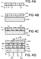
- FIG. 4A there is depicted a schematic cross-sectional view of a substrate 100 having a first surface 111 and an opposing second surface 112 in which openings 114 of a width dimension W extend from the second surface to the first surface.
- the previously described heat insulating layer 13 is not used.
- FIG. 4B there is depicted the substrate 100 and a light transmissive support 200 having a light absorbing layer 215 disposed on an upper surface thereof.
- the light absorbing layer 215 on the light transmissive support 200 is shown in contact with the second surface 112 of the substrate 100.
- a color forming organic donor layer 116 is formed in the openings 114 on the light absorbing layer 215 and on the first surface 111 between the openings 114.
- the donor layer 116 can be formed by vapor deposition from a collimated vapor source.
- FIG. 4D there is shown in a schematic cross-sectional view, the method for selective transfer of a color organic layer depicted in FIG. 4C in which a radiation exposure 400 is incident on the light transmissive support 200 and is absorbed by the light absorbing layer 215, thereby causing vaporization of the color forming organic donor layer previously disposed on the light absorbing layer within the openings 114 in the substrate 100.
- the transfer of the color forming organic donor layer through the openings 114 is schematically indicated by dotted arrows, and provides a selectively transferred color organic layer 336 on designated pixels 332 of a device 300, which is shown for illustrative purposes only to be spaced from an upper surface of the donor layer 116 between the openings 114.
- the device 300 is positioned prior to exposure in contact or close proximity to the upper surface of the donor layer 116 in an oriented relationship between the pixels 332 and corresponding openings 114 in the substrate, with close proximity being a spacing smaller than or equal to W p for full pixel coverage, where W ⁇ W p , or is smaller than or equal to W for fractional pixel coverage of EL display devices where W ⁇ W p , as detailed above in the discussion of FIG. 2E.
- the exposure 400 can be a blanket exposure provided by a pulsed gas discharge lamp and, alternatively, it can be radiation from a scanning laser light beam.
- the light transmissive support 200 with the light absorbing layer 215 thereon can be bonded to the second surface 112 of the substrate 100.
- donor layer residue is removed from the substrate by suitable cleaning processes.
- a donor layer capable of forming another color for example, a green color
- the device is repositioned via orientation marks with respect to the donor layer of such other color in an oriented relationship between the openings 14 (114) and the designated subpixels 32 (332) corresponding to the other color.
- Selective transfer of this donor layer to the designated subpixels of the device then commences by employing a source of radiation as detailed above.
- the sequence of cleaning, donor layer deposition, device repositioning, and selective donor layer transfer is repeated to form the third color (for example, a blue color) organic layer on the corresponding designated subpixels of the device 30 (300).
- the plurality of openings 14 or 114 depicted in FIG. 1 are shown for illustrative purposes only.
- the number of openings, the shape of openings, and the spacing between openings, also referred to as pitch, in a method in accordance with the present invention will be selected to match the number, shape, and pitch of pixels of a device which is to receive the selectively transferred color organic layer.
- both image sensing and organic EL display devices are available in numerous differing configurations. Accordingly, the method for selectively transferring a color organic layer to designated pixels or subpixels of a particular one of such numerous devices will be adapted to be operative with respect to such a particular device.
- the method further including a light transmissive support for supporting the second surface of the substrate having the openings.
- the radiation source includes a light source which provides a blanket radiation exposure.
- the radiation source includes a scanning light source.
- the substrate is selected from the group consisting of a silicon wafer, a glass plate, and a ceramic plate.
Landscapes
- Physics & Mathematics (AREA)
- Optics & Photonics (AREA)
- General Physics & Mathematics (AREA)
- Engineering & Computer Science (AREA)
- Manufacturing & Machinery (AREA)
- Electroluminescent Light Sources (AREA)
- Optical Filters (AREA)
- Liquid Crystal (AREA)
- Printers Or Recording Devices Using Electromagnetic And Radiation Means (AREA)
Applications Claiming Priority (2)
| Application Number | Priority Date | Filing Date | Title |
|---|---|---|---|
| US08/961,808 US5851709A (en) | 1997-10-31 | 1997-10-31 | Method for selective transfer of a color organic layer |
| US961808 | 1997-10-31 |
Publications (2)
| Publication Number | Publication Date |
|---|---|
| EP0913870A2 true EP0913870A2 (fr) | 1999-05-06 |
| EP0913870A3 EP0913870A3 (fr) | 2000-02-09 |
Family
ID=25505046
Family Applications (1)
| Application Number | Title | Priority Date | Filing Date |
|---|---|---|---|
| EP98203510A Withdrawn EP0913870A3 (fr) | 1997-10-31 | 1998-10-19 | Méthode de transfert sélectif d'une couche organique colorée |
Country Status (3)
| Country | Link |
|---|---|
| US (1) | US5851709A (fr) |
| EP (1) | EP0913870A3 (fr) |
| JP (1) | JPH11237504A (fr) |
Cited By (13)
| Publication number | Priority date | Publication date | Assignee | Title |
|---|---|---|---|---|
| EP1335637A1 (fr) * | 2002-01-30 | 2003-08-13 | Eastman Kodak Company | Procédé de fabrication des dispositifs electroluminescents |
| EP1646094A1 (fr) * | 2004-10-05 | 2006-04-12 | Samsung SDI Co., Ltd. | Procédé de fabrication de substrat donneur et procédé de fabrication d'un OLED au moyen du substrat donneur |
| CN1310772C (zh) * | 2002-08-02 | 2007-04-18 | 伊斯曼柯达公司 | 包含分离的掺杂剂层的激光热转印给体 |
| EP1480282A3 (fr) * | 2003-05-22 | 2011-08-03 | Global OLED Technology LLC | Substrat donneur à humidité réduite sur lequel on dépose des couches organiques pour transfert par lumière incidente |
| US8277871B2 (en) | 2007-10-23 | 2012-10-02 | Semiconductor Energy Laboratory Co., Ltd. | Evaporation donor substrate and method for manufacturing light-emitting device |
| US8425974B2 (en) | 2007-11-29 | 2013-04-23 | Semiconductor Energy Laboratory Co., Ltd. | Evaporation donor substrate and method for manufacturing light-emitting device |
| US8435811B2 (en) | 2007-12-28 | 2013-05-07 | Semiconductor Energy Laboratory Co., Ltd. | Method for manufacturing evaporation donor substrate and light-emitting device |
| US8653543B2 (en) | 2008-04-14 | 2014-02-18 | Semiconductor Energy Laboratory Co., Ltd. | Deposition substrate and method for manufacturing light-emitting device |
| US8734915B2 (en) | 2008-02-29 | 2014-05-27 | Semiconductor Energy Laboratory Co., Ltd. | Film-formation method and manufacturing method of light-emitting device |
| US8821963B2 (en) | 2008-02-04 | 2014-09-02 | Semiconductor Energy Laboratory Co., Ltd. | Deposition method and method for manufacturing light-emitting device |
| US9159923B2 (en) | 2007-12-26 | 2015-10-13 | Semiconductor Energy Laboratory Co., Ltd. | Evaporation donor substrate, method for manufacturing the same, and method for manufacturing light-emitting device |
| US9444051B2 (en) | 2007-10-23 | 2016-09-13 | Semiconductor Energy Laboratory Co., Ltd. | Method of manufacturing light-emitting device, and evaporation donor substrate |
| CN110310573A (zh) * | 2019-06-27 | 2019-10-08 | 云谷(固安)科技有限公司 | 一种显示面板 |
Families Citing this family (117)
| Publication number | Priority date | Publication date | Assignee | Title |
|---|---|---|---|---|
| JP3019095B1 (ja) * | 1998-12-22 | 2000-03-13 | 日本電気株式会社 | 有機薄膜elデバイスの製造方法 |
| JP2002539485A (ja) * | 1999-03-08 | 2002-11-19 | コーニンクレッカ フィリップス エレクトロニクス エヌ ヴィ | 表示装置 |
| US6214151B1 (en) | 1999-11-05 | 2001-04-10 | International Business Machines Corporation | Thermal dye transfer process for preparing opto-electronic devices |
| KR100721656B1 (ko) | 2005-11-01 | 2007-05-23 | 주식회사 엘지화학 | 유기 전기 소자 |
| US6852355B2 (en) * | 2001-03-01 | 2005-02-08 | E. I. Du Pont De Nemours And Company | Thermal imaging processes and products of electroactive organic material |
| JP2002343565A (ja) | 2001-05-18 | 2002-11-29 | Sharp Corp | 有機led表示パネルの製造方法、その方法により製造された有機led表示パネル、並びに、その方法に用いられるベースフィルム及び基板 |
| JP2002343564A (ja) | 2001-05-18 | 2002-11-29 | Sharp Corp | 転写用フィルムおよびそれを用いた有機エレクトロルミネッセンス素子の製造方法 |
| US6695029B2 (en) | 2001-12-12 | 2004-02-24 | Eastman Kodak Company | Apparatus for permitting transfer of organic material from a donor to form a layer in an OLED device |
| US6688365B2 (en) | 2001-12-19 | 2004-02-10 | Eastman Kodak Company | Method for transferring of organic material from a donor to form a layer in an OLED device |
| US6555284B1 (en) | 2001-12-27 | 2003-04-29 | Eastman Kodak Company | In situ vacuum method for making OLED devices |
| US6582875B1 (en) | 2002-01-23 | 2003-06-24 | Eastman Kodak Company | Using a multichannel linear laser light beam in making OLED devices by thermal transfer |
| US6872472B2 (en) | 2002-02-15 | 2005-03-29 | Eastman Kodak Company | Providing an organic electroluminescent device having stacked electroluminescent units |
| US6703179B2 (en) | 2002-03-13 | 2004-03-09 | Eastman Kodak Company | Transfer of organic material from a donor to form a layer in an OLED device |
| US6770502B2 (en) * | 2002-04-04 | 2004-08-03 | Eastman Kodak Company | Method of manufacturing a top-emitting OLED display device with desiccant structures |
| US6566032B1 (en) | 2002-05-08 | 2003-05-20 | Eastman Kodak Company | In-situ method for making OLED devices that are moisture or oxygen-sensitive |
| US6682863B2 (en) * | 2002-06-27 | 2004-01-27 | Eastman Kodak Company | Depositing an emissive layer for use in an organic light-emitting display device (OLED) |
| TW200402012A (en) * | 2002-07-23 | 2004-02-01 | Eastman Kodak Co | OLED displays with fiber-optic faceplates |
| US6890627B2 (en) | 2002-08-02 | 2005-05-10 | Eastman Kodak Company | Laser thermal transfer from a donor element containing a hole-transporting layer |
| US6747618B2 (en) | 2002-08-20 | 2004-06-08 | Eastman Kodak Company | Color organic light emitting diode display with improved lifetime |
| US6695030B1 (en) | 2002-08-20 | 2004-02-24 | Eastman Kodak Company | Apparatus for permitting transfer of organic material from a donor web to form a layer in an OLED device |
| US6811938B2 (en) * | 2002-08-29 | 2004-11-02 | Eastman Kodak Company | Using fiducial marks on a substrate for laser transfer of organic material from a donor to a substrate |
| US6765349B2 (en) * | 2002-09-30 | 2004-07-20 | Eastman Kodak Company | High work function metal alloy cathode used in organic electroluminescent devices |
| US20040067302A1 (en) * | 2002-10-08 | 2004-04-08 | Eastman Kodak Company | Laser thermal transfer gap control for oled manufacturing |
| US6831407B2 (en) * | 2002-10-15 | 2004-12-14 | Eastman Kodak Company | Oled device having improved light output |
| US20040250769A1 (en) * | 2002-10-28 | 2004-12-16 | Finisar Corporation | Pulsed laser deposition for mass production |
| US6982179B2 (en) * | 2002-11-15 | 2006-01-03 | University Display Corporation | Structure and method of fabricating organic devices |
| US20040096570A1 (en) * | 2002-11-15 | 2004-05-20 | Michael Weaver | Structure and method of fabricating organic devices |
| US6896723B2 (en) * | 2002-12-06 | 2005-05-24 | Eastman Kodak Company | Compressed fluid formulation containing hole transporting material |
| US6927415B2 (en) * | 2002-12-06 | 2005-08-09 | Eastman Kodak Company | Compressed fluid formulation containing electron transporting material |
| US6896827B2 (en) * | 2002-12-06 | 2005-05-24 | Eastman Kodak Company | Compressed fluid formulation containing electroluminescent polymeric material |
| US6918982B2 (en) * | 2002-12-09 | 2005-07-19 | International Business Machines Corporation | System and method of transfer printing an organic semiconductor |
| US7230594B2 (en) | 2002-12-16 | 2007-06-12 | Eastman Kodak Company | Color OLED display with improved power efficiency |
| US6777025B2 (en) * | 2002-12-20 | 2004-08-17 | Eastman Kodak Company | Tensioning unrolled donor substrate to facilitate transfer of organic material |
| US7052351B2 (en) * | 2002-12-31 | 2006-05-30 | Eastman Kodak Company | Using hole- or electron-blocking layers in color OLEDS |
| US6824950B2 (en) * | 2003-02-14 | 2004-11-30 | Eastman Kodak Company | Forming an oled device with a performance-inhancing layer |
| US7026658B2 (en) * | 2003-03-13 | 2006-04-11 | Samsung Sdi, Co., Ltd. | Electrical conductors in an electroluminescent display device |
| US6790594B1 (en) | 2003-03-20 | 2004-09-14 | Eastman Kodak Company | High absorption donor substrate coatable with organic layer(s) transferrable in response to incident laser light |
| US7033711B2 (en) * | 2003-07-16 | 2006-04-25 | Eastman Kodak Company | Aperture ratio or resolution of an OLED device by limiting the edge taper region |
| US6929048B2 (en) * | 2003-09-05 | 2005-08-16 | Eastman Kodak Company | Laser transfer of organic material from a donor to form a layer in an OLED device |
| US7221332B2 (en) * | 2003-12-19 | 2007-05-22 | Eastman Kodak Company | 3D stereo OLED display |
| US7381579B2 (en) * | 2004-02-26 | 2008-06-03 | Samsung Sdi Co., Ltd. | Donor sheet, method of manufacturing the same, method of manufacturing TFT using the donor sheet, and method of manufacturing flat panel display device using the donor sheet |
| US7238252B2 (en) * | 2004-03-02 | 2007-07-03 | Eastman Kodak Company | Method of forming a OLED donor sheet having rigid edge frame |
| US7032285B2 (en) * | 2004-03-02 | 2006-04-25 | Eastman Kodak Company | Mounting an OLED donor sheet to frames |
| US7132140B2 (en) * | 2004-05-27 | 2006-11-07 | Eastman Kodak Company | Plural metallic layers in OLED donor |
| US7291365B2 (en) * | 2004-05-27 | 2007-11-06 | Eastman Kodak Company | Linear laser light beam for making OLEDS |
| US20060017055A1 (en) * | 2004-07-23 | 2006-01-26 | Eastman Kodak Company | Method for manufacturing a display device with low temperature diamond coatings |
| KR20060020045A (ko) * | 2004-08-30 | 2006-03-06 | 삼성에스디아이 주식회사 | 유기전계발광표시장치의 제조방법 |
| US9040170B2 (en) * | 2004-09-20 | 2015-05-26 | Global Oled Technology Llc | Electroluminescent device with quinazoline complex emitter |
| KR100667069B1 (ko) * | 2004-10-19 | 2007-01-10 | 삼성에스디아이 주식회사 | 도너 기판 및 그를 사용한 유기전계발광표시장치의 제조방법 |
| US8057916B2 (en) | 2005-04-20 | 2011-11-15 | Global Oled Technology, Llc. | OLED device with improved performance |
| US20060240281A1 (en) * | 2005-04-21 | 2006-10-26 | Eastman Kodak Company | Contaminant-scavenging layer on OLED anodes |
| US20060273713A1 (en) * | 2005-06-02 | 2006-12-07 | Eastman Kodak Company | Process for making an organic light-emitting device |
| US20070048545A1 (en) * | 2005-08-31 | 2007-03-01 | Eastman Kodak Company | Electron-transporting layer for white OLED device |
| US8956738B2 (en) | 2005-10-26 | 2015-02-17 | Global Oled Technology Llc | Organic element for low voltage electroluminescent devices |
| US9666826B2 (en) | 2005-11-30 | 2017-05-30 | Global Oled Technology Llc | Electroluminescent device including an anthracene derivative |
| US20070122657A1 (en) * | 2005-11-30 | 2007-05-31 | Eastman Kodak Company | Electroluminescent device containing a phenanthroline derivative |
| US8680693B2 (en) | 2006-01-18 | 2014-03-25 | Lg Chem. Ltd. | OLED having stacked organic light-emitting units |
| US9118020B2 (en) | 2006-04-27 | 2015-08-25 | Global Oled Technology Llc | Electroluminescent devices including organic eil layer |
| EP2016633A1 (fr) | 2006-05-08 | 2009-01-21 | Eastman Kodak Company | Couche d'injection d'electrons d'une oled |
| US20080131587A1 (en) * | 2006-11-30 | 2008-06-05 | Boroson Michael L | Depositing organic material onto an oled substrate |
| WO2008069259A1 (fr) * | 2006-12-05 | 2008-06-12 | Semiconductor Energy Laboratory Co., Ltd. | Appareil de formation d'un film, procédé de formation d'un film, appareil de fabrication et procédé de fabrication d'un dispositif électroluminescent |
| US8795855B2 (en) | 2007-01-30 | 2014-08-05 | Global Oled Technology Llc | OLEDs having high efficiency and excellent lifetime |
| US8034465B2 (en) * | 2007-06-20 | 2011-10-11 | Global Oled Technology Llc | Phosphorescent oled having double exciton-blocking layers |
| US20090004485A1 (en) * | 2007-06-27 | 2009-01-01 | Shiying Zheng | 6-member ring structure used in electroluminescent devices |
| KR20090028413A (ko) * | 2007-09-13 | 2009-03-18 | 가부시키가이샤 한도오따이 에네루기 켄큐쇼 | 발광장치 제작방법 및 증착용 기판 |
| JP5669580B2 (ja) * | 2007-09-20 | 2015-02-12 | ビーエーエスエフ ソシエタス・ヨーロピアBasf Se | エレクトロルミネセンスデバイス |
| US8420229B2 (en) * | 2007-10-26 | 2013-04-16 | Global OLED Technologies LLC | OLED device with certain fluoranthene light-emitting dopants |
| US8129039B2 (en) | 2007-10-26 | 2012-03-06 | Global Oled Technology, Llc | Phosphorescent OLED device with certain fluoranthene host |
| US8076009B2 (en) | 2007-10-26 | 2011-12-13 | Global Oled Technology, Llc. | OLED device with fluoranthene electron transport materials |
| US8431242B2 (en) | 2007-10-26 | 2013-04-30 | Global Oled Technology, Llc. | OLED device with certain fluoranthene host |
| US8900722B2 (en) | 2007-11-29 | 2014-12-02 | Global Oled Technology Llc | OLED device employing alkali metal cluster compounds |
| US20090162612A1 (en) * | 2007-12-19 | 2009-06-25 | Hatwar Tukaram K | Oled device having two electron-transport layers |
| US20090191427A1 (en) * | 2008-01-30 | 2009-07-30 | Liang-Sheng Liao | Phosphorescent oled having double hole-blocking layers |
| JP2009231277A (ja) * | 2008-02-29 | 2009-10-08 | Semiconductor Energy Lab Co Ltd | 製造装置 |
| WO2009107548A1 (fr) * | 2008-02-29 | 2009-09-03 | Semiconductor Energy Laboratory Co., Ltd. | Procédé de dépôt et procédé de fabrication de dispositif électroluminescent |
| JP5367415B2 (ja) * | 2008-03-06 | 2013-12-11 | 株式会社半導体エネルギー研究所 | 発光装置の作製方法及び成膜用基板 |
| JP5238544B2 (ja) * | 2008-03-07 | 2013-07-17 | 株式会社半導体エネルギー研究所 | 成膜方法及び発光装置の作製方法 |
| JP5079722B2 (ja) * | 2008-03-07 | 2012-11-21 | 株式会社半導体エネルギー研究所 | 発光装置の作製方法 |
| US8182863B2 (en) * | 2008-03-17 | 2012-05-22 | Semiconductor Energy Laboratory Co., Ltd. | Deposition method and manufacturing method of light-emitting device |
| US7947974B2 (en) * | 2008-03-25 | 2011-05-24 | Global Oled Technology Llc | OLED device with hole-transport and electron-transport materials |
| US8409672B2 (en) * | 2008-04-24 | 2013-04-02 | Semiconductor Energy Laboratory Co., Ltd. | Method of manufacturing evaporation donor substrate and method of manufacturing light-emitting device |
| JP5159689B2 (ja) * | 2008-04-25 | 2013-03-06 | 株式会社半導体エネルギー研究所 | 発光装置の作製方法 |
| KR101629637B1 (ko) * | 2008-05-29 | 2016-06-13 | 가부시키가이샤 한도오따이 에네루기 켄큐쇼 | 성막방법 및 발광장치의 제조방법 |
| US7919340B2 (en) * | 2008-06-04 | 2011-04-05 | Semiconductor Energy Laboratory Co., Ltd. | Method for manufacturing light-emitting device |
| US8324800B2 (en) * | 2008-06-12 | 2012-12-04 | Global Oled Technology Llc | Phosphorescent OLED device with mixed hosts |
| US8574709B2 (en) * | 2008-07-21 | 2013-11-05 | Semiconductor Energy Laboratory Co., Ltd. | Deposition donor substrate and method for manufacturing light-emitting device |
| JP5469950B2 (ja) * | 2008-08-08 | 2014-04-16 | 株式会社半導体エネルギー研究所 | 発光装置の作製方法 |
| US8247088B2 (en) * | 2008-08-28 | 2012-08-21 | Global Oled Technology Llc | Emitting complex for electroluminescent devices |
| EP2161272A1 (fr) | 2008-09-05 | 2010-03-10 | Basf Se | Phénanthrolines |
| US8486736B2 (en) * | 2008-10-20 | 2013-07-16 | Semiconductor Energy Laboratory Co., Ltd. | Method for manufacturing light-emitting device |
| US7931975B2 (en) | 2008-11-07 | 2011-04-26 | Global Oled Technology Llc | Electroluminescent device containing a flouranthene compound |
| US8088500B2 (en) | 2008-11-12 | 2012-01-03 | Global Oled Technology Llc | OLED device with fluoranthene electron injection materials |
| US7968215B2 (en) | 2008-12-09 | 2011-06-28 | Global Oled Technology Llc | OLED device with cyclobutene electron injection materials |
| JP5438313B2 (ja) * | 2008-12-23 | 2014-03-12 | 株式会社半導体エネルギー研究所 | 成膜方法 |
| US8216697B2 (en) * | 2009-02-13 | 2012-07-10 | Global Oled Technology Llc | OLED with fluoranthene-macrocyclic materials |
| US8147989B2 (en) | 2009-02-27 | 2012-04-03 | Global Oled Technology Llc | OLED device with stabilized green light-emitting layer |
| US20100244677A1 (en) * | 2009-03-31 | 2010-09-30 | Begley William J | Oled device containing a silyl-fluoranthene derivative |
| US8206842B2 (en) | 2009-04-06 | 2012-06-26 | Global Oled Technology Llc | Organic element for electroluminescent devices |
| JP2010251360A (ja) * | 2009-04-10 | 2010-11-04 | Sony Corp | 表示装置の製造方法および表示装置 |
| JP5111427B2 (ja) * | 2009-04-16 | 2013-01-09 | 株式会社半導体エネルギー研究所 | 成膜用基板および成膜方法 |
| JP5258666B2 (ja) * | 2009-04-22 | 2013-08-07 | 株式会社半導体エネルギー研究所 | 発光装置の作製方法および成膜用基板 |
| CN102482574B (zh) | 2009-06-18 | 2014-09-24 | 巴斯夫欧洲公司 | 用作场致发光器件的空穴传输材料的菲并唑化合物 |
| US8877356B2 (en) * | 2009-07-22 | 2014-11-04 | Global Oled Technology Llc | OLED device with stabilized yellow light-emitting layer |
| JP5323784B2 (ja) * | 2009-09-15 | 2013-10-23 | フオン・アルデンネ・アンラーゲンテヒニク・ゲゼルシヤフト・ミト・ベシユレンクテル・ハフツング | 微細構造を製造するための方法及び装置 |
| US8242489B2 (en) | 2009-12-17 | 2012-08-14 | Global Oled Technology, Llc. | OLED with high efficiency blue light-emitting layer |
| US8288187B2 (en) * | 2010-01-20 | 2012-10-16 | Universal Display Corporation | Electroluminescent devices for lighting applications |
| JP5731063B2 (ja) | 2011-04-08 | 2015-06-10 | エーエスエムエル ネザーランズ ビー.ブイ. | リソグラフィ装置、プログラマブル・パターニングデバイス、及びリソグラフィ方法 |
| CN103676309B (zh) * | 2012-09-10 | 2016-08-17 | 联想(北京)有限公司 | 显示装置 |
| CN104752632B (zh) * | 2013-12-31 | 2017-03-08 | 昆山工研院新型平板显示技术中心有限公司 | 一种有机发光显示器的像素的制造方法 |
| KR102181239B1 (ko) * | 2014-09-03 | 2020-11-23 | 삼성디스플레이 주식회사 | 박막 형성 장치 및 그를 이용한 박막 형성 방법 |
| JP6756125B2 (ja) * | 2016-03-16 | 2020-09-16 | 富士電機株式会社 | 半導体装置および半導体装置の製造方法 |
| US10727449B2 (en) | 2016-06-24 | 2020-07-28 | Pioneer Corporation | Light-emitting device |
| KR101929409B1 (ko) * | 2016-12-22 | 2018-12-14 | 주식회사 다원시스 | 유기 발광 장치용 유기물 증착 방법 및 유기 발광 장치 |
| US11360386B2 (en) * | 2016-12-22 | 2022-06-14 | Toray Industries, Inc. | Organic EL display device |
| CN110224014B (zh) * | 2019-06-21 | 2021-12-28 | 京东方科技集团股份有限公司 | 一种图案的制备方法及显示基板的制备方法 |
| KR102921492B1 (ko) * | 2021-05-06 | 2026-02-02 | 삼성디스플레이 주식회사 | 표시 장치의 제조장치 |
| EP4340552A1 (fr) * | 2022-09-13 | 2024-03-20 | Mycronic Ab | Procédé et dispositif de transfert vers l'avant induit par laser |
Family Cites Families (8)
| Publication number | Priority date | Publication date | Assignee | Title |
|---|---|---|---|---|
| DE3023131A1 (de) * | 1979-06-20 | 1981-01-08 | Canon Kk | Verfahren zum herstellen eines farbfilters |
| US4769292A (en) * | 1987-03-02 | 1988-09-06 | Eastman Kodak Company | Electroluminescent device with modified thin film luminescent zone |
| US5405709A (en) * | 1993-09-13 | 1995-04-11 | Eastman Kodak Company | White light emitting internal junction organic electroluminescent device |
| US5521035A (en) * | 1994-07-11 | 1996-05-28 | Minnesota Mining And Manufacturing Company | Methods for preparing color filter elements using laser induced transfer of colorants with associated liquid crystal display device |
| JPH08152512A (ja) * | 1994-11-30 | 1996-06-11 | Toppan Printing Co Ltd | 画像形成方法およびカラーフィルタの製造方法 |
| US5576265A (en) * | 1995-04-26 | 1996-11-19 | Eastman Kodak Company | Color filter arrays by stencil printing |
| US5688551A (en) * | 1995-11-13 | 1997-11-18 | Eastman Kodak Company | Method of forming an organic electroluminescent display panel |
| US5683823A (en) * | 1996-01-26 | 1997-11-04 | Eastman Kodak Company | White light-emitting organic electroluminescent devices |
-
1997
- 1997-10-31 US US08/961,808 patent/US5851709A/en not_active Expired - Lifetime
-
1998
- 1998-10-19 EP EP98203510A patent/EP0913870A3/fr not_active Withdrawn
- 1998-10-30 JP JP31121598A patent/JPH11237504A/ja active Pending
Cited By (15)
| Publication number | Priority date | Publication date | Assignee | Title |
|---|---|---|---|---|
| EP1335637A1 (fr) * | 2002-01-30 | 2003-08-13 | Eastman Kodak Company | Procédé de fabrication des dispositifs electroluminescents |
| CN1310772C (zh) * | 2002-08-02 | 2007-04-18 | 伊斯曼柯达公司 | 包含分离的掺杂剂层的激光热转印给体 |
| EP1480282A3 (fr) * | 2003-05-22 | 2011-08-03 | Global OLED Technology LLC | Substrat donneur à humidité réduite sur lequel on dépose des couches organiques pour transfert par lumière incidente |
| EP1646094A1 (fr) * | 2004-10-05 | 2006-04-12 | Samsung SDI Co., Ltd. | Procédé de fabrication de substrat donneur et procédé de fabrication d'un OLED au moyen du substrat donneur |
| US7223514B2 (en) | 2004-10-05 | 2007-05-29 | Samsung Sdi Co., Ltd. | Method of fabricating donor substrate and method of fabricating OLED using the donor substrate |
| US9444051B2 (en) | 2007-10-23 | 2016-09-13 | Semiconductor Energy Laboratory Co., Ltd. | Method of manufacturing light-emitting device, and evaporation donor substrate |
| US8277871B2 (en) | 2007-10-23 | 2012-10-02 | Semiconductor Energy Laboratory Co., Ltd. | Evaporation donor substrate and method for manufacturing light-emitting device |
| US8425974B2 (en) | 2007-11-29 | 2013-04-23 | Semiconductor Energy Laboratory Co., Ltd. | Evaporation donor substrate and method for manufacturing light-emitting device |
| US9159923B2 (en) | 2007-12-26 | 2015-10-13 | Semiconductor Energy Laboratory Co., Ltd. | Evaporation donor substrate, method for manufacturing the same, and method for manufacturing light-emitting device |
| US8435811B2 (en) | 2007-12-28 | 2013-05-07 | Semiconductor Energy Laboratory Co., Ltd. | Method for manufacturing evaporation donor substrate and light-emitting device |
| US8821963B2 (en) | 2008-02-04 | 2014-09-02 | Semiconductor Energy Laboratory Co., Ltd. | Deposition method and method for manufacturing light-emitting device |
| US8734915B2 (en) | 2008-02-29 | 2014-05-27 | Semiconductor Energy Laboratory Co., Ltd. | Film-formation method and manufacturing method of light-emitting device |
| US8653543B2 (en) | 2008-04-14 | 2014-02-18 | Semiconductor Energy Laboratory Co., Ltd. | Deposition substrate and method for manufacturing light-emitting device |
| CN110310573A (zh) * | 2019-06-27 | 2019-10-08 | 云谷(固安)科技有限公司 | 一种显示面板 |
| CN110310573B (zh) * | 2019-06-27 | 2021-07-23 | 云谷(固安)科技有限公司 | 一种显示面板 |
Also Published As
| Publication number | Publication date |
|---|---|
| US5851709A (en) | 1998-12-22 |
| JPH11237504A (ja) | 1999-08-31 |
| EP0913870A3 (fr) | 2000-02-09 |
Similar Documents
| Publication | Publication Date | Title |
|---|---|---|
| US5851709A (en) | Method for selective transfer of a color organic layer | |
| JP3789991B2 (ja) | 有機エレクトロルミネセンス媒体を熱転写するためのドナーシート及びフルカラー有機エレクトロルミネセンス表示装置の製造方法 | |
| JP2002110350A (ja) | 有機電界発光表示装置の製造方法 | |
| KR100298272B1 (ko) | 칼라유기el 디스플레이 및 그 제조방법 | |
| US5756240A (en) | Method of making color filter arrays by transferring colorant material | |
| US5229232A (en) | Method of making thermally-transferred color filter arrays with incorporated black matrix using electronic light flash | |
| JPH1154275A (ja) | 薄膜トランジスタ配列基板上のフルカラー有機エレクトロルミネセンス表示配列にパターン化された有機層 | |
| US20080026303A1 (en) | Donor sheet, color filter, organic el element and method for producing them | |
| KR20000064839A (ko) | 유기 전압 발광 표시 장치 | |
| KR20000048257A (ko) | 전색 유기성 발광 디스플레이 제조방법 | |
| KR20120113747A (ko) | 도너 기판, 패터닝 방법 및 디바이스의 제조 방법 | |
| US20220352430A1 (en) | Micro light emitting diode array and manufacturing method thereof | |
| US20040012020A1 (en) | Integral organic light emitting diode printhead utilizing color filters | |
| EP0771673B1 (fr) | Méthode pour la fabrication d'un élément de filtre-réseaux colorés | |
| MXPA06005650A (es) | Metodo para fabricar dispositivo electroluminiscente que incluye filtro de color. | |
| JPH0752244B2 (ja) | イエロー染料とシアン染料からなるカラーフィルターアレイ素子の緑色用混合物 | |
| JPH0816723B2 (ja) | カラーフィルターアレイ素子用アリールアゾアニリンブルー染料 | |
| JPH05173016A (ja) | イエロー染料とマゼンタ染料からなるカラーフィルターアレイ素子の赤色用混合物 | |
| EP0518349B1 (fr) | Mélange de colorants cyans et jaunes pour former une teinte verte pour élément de filtre-réseaux colorés | |
| US6214151B1 (en) | Thermal dye transfer process for preparing opto-electronic devices | |
| JP2504693B2 (ja) | 感熱転写カラ―フィルタ―アレイ素子 | |
| JP2006163241A (ja) | 有機エレクトロルミネッセント素子用カラーフィルタ基板 | |
| FR2678391A1 (fr) | Procede de depot local d'un materiau par impression thermo-optique et application de ce procede a la fabrication de filtres colores. |
Legal Events
| Date | Code | Title | Description |
|---|---|---|---|
| PUAI | Public reference made under article 153(3) epc to a published international application that has entered the european phase |
Free format text: ORIGINAL CODE: 0009012 |
|
| AK | Designated contracting states |
Kind code of ref document: A2 Designated state(s): DE FR GB |
|
| AX | Request for extension of the european patent |
Free format text: AL;LT;LV;MK;RO;SI |
|
| PUAL | Search report despatched |
Free format text: ORIGINAL CODE: 0009013 |
|
| AK | Designated contracting states |
Kind code of ref document: A3 Designated state(s): AT BE CH CY DE DK ES FI FR GB GR IE IT LI LU MC NL PT SE |
|
| AX | Request for extension of the european patent |
Free format text: AL;LT;LV;MK;RO;SI |
|
| 17P | Request for examination filed |
Effective date: 20000713 |
|
| AKX | Designation fees paid |
Free format text: DE FR GB |
|
| GRAP | Despatch of communication of intention to grant a patent |
Free format text: ORIGINAL CODE: EPIDOSNIGR1 |
|
| 18D | Application deemed to be withdrawn |
Effective date: 20060327 |