EP1646151A1 - Procede de reechantillonnage dans la transmission et la reception d'un signal numerique avec translation dans la bande numerique - Google Patents
Procede de reechantillonnage dans la transmission et la reception d'un signal numerique avec translation dans la bande numerique Download PDFInfo
- Publication number
- EP1646151A1 EP1646151A1 EP04735485A EP04735485A EP1646151A1 EP 1646151 A1 EP1646151 A1 EP 1646151A1 EP 04735485 A EP04735485 A EP 04735485A EP 04735485 A EP04735485 A EP 04735485A EP 1646151 A1 EP1646151 A1 EP 1646151A1
- Authority
- EP
- European Patent Office
- Prior art keywords
- signal
- transmission
- digital
- resampling
- reception
- Prior art date
- Legal status (The legal status is an assumption and is not a legal conclusion. Google has not performed a legal analysis and makes no representation as to the accuracy of the status listed.)
- Granted
Links
- 238000012952 Resampling Methods 0.000 title claims abstract description 60
- 230000005540 biological transmission Effects 0.000 title claims abstract description 57
- 238000013519 translation Methods 0.000 title claims abstract description 41
- 238000000034 method Methods 0.000 title claims abstract description 29
- 238000005070 sampling Methods 0.000 claims description 16
- 238000012545 processing Methods 0.000 claims description 14
- 238000004364 calculation method Methods 0.000 claims description 4
- 238000006243 chemical reaction Methods 0.000 claims description 4
- 238000013461 design Methods 0.000 claims description 2
- 238000012937 correction Methods 0.000 abstract description 12
- 230000014616 translation Effects 0.000 description 25
- 238000004891 communication Methods 0.000 description 8
- 230000008569 process Effects 0.000 description 6
- 239000000523 sample Substances 0.000 description 6
- 238000004422 calculation algorithm Methods 0.000 description 5
- 230000006870 function Effects 0.000 description 3
- 238000010586 diagram Methods 0.000 description 2
- 238000007620 mathematical function Methods 0.000 description 1
- 230000009467 reduction Effects 0.000 description 1
- 230000004044 response Effects 0.000 description 1
Images


Classifications
-
- H—ELECTRICITY
- H03—ELECTRONIC CIRCUITRY
- H03M—CODING; DECODING; CODE CONVERSION IN GENERAL
- H03M1/00—Analogue/digital conversion; Digital/analogue conversion
- H03M1/06—Continuously compensating for, or preventing, undesired influence of physical parameters
- H03M1/08—Continuously compensating for, or preventing, undesired influence of physical parameters of noise
- H03M1/0836—Continuously compensating for, or preventing, undesired influence of physical parameters of noise of phase error, e.g. jitter
-
- H—ELECTRICITY
- H04—ELECTRIC COMMUNICATION TECHNIQUE
- H04L—TRANSMISSION OF DIGITAL INFORMATION, e.g. TELEGRAPHIC COMMUNICATION
- H04L27/00—Modulated-carrier systems
-
- H—ELECTRICITY
- H03—ELECTRONIC CIRCUITRY
- H03M—CODING; DECODING; CODE CONVERSION IN GENERAL
- H03M1/00—Analogue/digital conversion; Digital/analogue conversion
- H03M1/06—Continuously compensating for, or preventing, undesired influence of physical parameters
-
- H—ELECTRICITY
- H03—ELECTRONIC CIRCUITRY
- H03M—CODING; DECODING; CODE CONVERSION IN GENERAL
- H03M1/00—Analogue/digital conversion; Digital/analogue conversion
- H03M1/66—Digital/analogue converters
-
- H—ELECTRICITY
- H03—ELECTRONIC CIRCUITRY
- H03M—CODING; DECODING; CODE CONVERSION IN GENERAL
- H03M3/00—Conversion of analogue values to or from differential modulation
- H03M3/30—Delta-sigma modulation
- H03M3/322—Continuously compensating for, or preventing, undesired influence of physical parameters
- H03M3/368—Continuously compensating for, or preventing, undesired influence of physical parameters of noise other than the quantisation noise already being shaped inherently by delta-sigma modulators
- H03M3/37—Compensation or reduction of delay or phase error
-
- H—ELECTRICITY
- H03—ELECTRONIC CIRCUITRY
- H03M—CODING; DECODING; CODE CONVERSION IN GENERAL
- H03M7/00—Conversion of a code where information is represented by a given sequence or number of digits to a code where the same, similar or subset of information is represented by a different sequence or number of digits
-
- H—ELECTRICITY
- H03—ELECTRONIC CIRCUITRY
- H03M—CODING; DECODING; CODE CONVERSION IN GENERAL
- H03M1/00—Analogue/digital conversion; Digital/analogue conversion
- H03M1/12—Analogue/digital converters
-
- H—ELECTRICITY
- H03—ELECTRONIC CIRCUITRY
- H03M—CODING; DECODING; CODE CONVERSION IN GENERAL
- H03M3/00—Conversion of analogue values to or from differential modulation
- H03M3/30—Delta-sigma modulation
- H03M3/458—Analogue/digital converters using delta-sigma modulation as an intermediate step
- H03M3/462—Details relating to the decimation process
-
- H—ELECTRICITY
- H03—ELECTRONIC CIRCUITRY
- H03M—CODING; DECODING; CODE CONVERSION IN GENERAL
- H03M3/00—Conversion of analogue values to or from differential modulation
- H03M3/30—Delta-sigma modulation
- H03M3/50—Digital/analogue converters using delta-sigma modulation as an intermediate step
- H03M3/508—Details relating to the interpolation process
Definitions
- the present invention refers to a procedure for resampling in transmission and reception of a digital signal with digital band translation which permits correction of the frequency error introduced by digital-analog and analog-digital converters used in telecommunications systems.
- the procedure of the invention simplifies the electronics necessary for carrying out resampling in band-pass signals.
- the signal transmitted is sampled in reception by an analog-digital converter using a time constant sampling frequency.
- this sampling frequency is not exactly equal to the transmission frequency, it is necessary to interpolate the received signal in order to obtain the samples which would be received if the two frequencies were equal, and in this way be able to demodulate the previously transmitted data correctly.
- the invention forming the object of the patent proposes a variation on the interpolation structure which facilitates its implementation, reducing the complexity of the filters and lowering their working frequency. Also, the resampling is done not just in reception but also in transmission.
- CORDIC Coordinat Rotation Digital Computer
- the invention consists of a procedure for resampling in transmission and reception of a digital signal with digital band translation, which selectively comprises processing in transmission, in reception or a combination of both.
- the processing comprises the sampling of the signal in reception by means of an analog-digital converter (ADC), a band translation of the signal and a processing of the signal in the time domain. Due to the fact that most communications channels are band-pass channels, the information is transmitted in band-pass so that in reception, following the analog-digital conversion (ADC), a translation of the digital signal to base-band is performed.
- ADC analog-digital converter
- the invention provides for an adjustment to be made in reception to the band translation frequency of the digital signal in the process of conversion of the signal to base-band, and following that conversion the signal is decimated in order to reduce the sampling frequency and eliminate replicas. Following decimation of the signal in base-band, the signal is resampled in order to obtain the desired samples.
- the processing of the signal carried out in reception following the resampling is done continuously and the blocks located after the resampler must be capable of absorbing the variations in the output frequency of the signal from the resampler, for which an overdimensioning of the hardware is carried out.
- the base-band signal is resampled. Following the resampling, the signal is interpolated in order to increment the sampling frequency. Later on, the signal is translated in frequency in order to obtain a band-pass signal and supply it to the digital-analog converter (DAC) where the signal is converted into an analog signal for its transmission.
- DAC digital-analog converter
- the invention provides for the adjustment of the band translation frequency of the digital signal.
- a memory has been introduced after the resampler which is in charge of absorbing all the samples of the resampling block and supplying them to the interpolation block with a fixed cadence.
- the speed with which the samples are introduced into the memory is variable and the speed of reading the memory is fixed.
- the reading and writing indices will be reset to their initial valueswhen there is no transmission or just zeros are being transmitted.
- the calculation of the dimensions of the memory is done taking as reference the maximum transmission time and the maximum resampling time, in such a way that no sample that is introduced into that memory is lost.
- the signal is interpolated by an integer number prior to its application to the input of the resampler, while at its output the samples will be decimated by the same factor.
- the signal is transmitted in band-pass, in other words occupying a range of frequencies that does not include the frequency zero.
- this signal is internally processed in base-band, in other words, in a range of frequencies that includes zero, and it is then translated to band-pass in transmission. In reception the process is carried out in reverse.
- This resampling is normally done directly with the band-pass signal after sampling the reception signal by means of an ADC (1), in other words, directly using a resampler block (6), therefore the electronics that is used has to function at the same frequency generated by the oscillator (2) of the ADC converter, and the resampling filters have to have sufficient bandwidth in order not to distort the signal.
- the procedure of the invention uses a set of blocks (25) in order to achieve the resampling of the signal, with the advantages stated above. In transmission, the process is similar but the resampling block (16) conventionally used is replaced by the set of blocks (26) in order to carry out the resampling following the procedure of the invention.
- the system In the case of band-pass signals, the system is being overdimensioned because it is working at much higher frequencies than those which would be used if it were working in base-band. Therefore, in reception it is better to carry out the translation to base-band by means of a band translation block (4) directly after the ADC (1).
- the block (4) corresponds to two multipliers, one of the signal with sine and the other with cosine.
- a band translation block (20) is also used, which is carried out in a similar way, though adding an adder. This frequency translation is not fixed since it depends on the error introduced in the converters, so it has to be adjusted depending on the error that is being corrected.
- the invention After the frequency translation, the invention performs a decimation (5) of the signal by an integer number, N, in order to reduce the sampling frequency at the decimator output and eliminate the replicas appearing with the band translation, and after that the resampling of the signal is carried out.
- the resampling block (6) is known in the state of the art and it can be carried out in different ways like those described in part II of the article referenced in the background. By working at a lower frequency and the fact that it depends on the decimation factor, N, the design and the embodiment of the resampling filters become simpler.
- FIG. 1 Also appearing in figure 1 is a block (7) which is responsible for determining the frequency correction to apply and which, as has been explained, affects the translation to base-band, by means of varying the translation frequency to base-band via a CORDIC (3), and also affects the resampling block (6) which, as has been said, is known in the state of the art and which obtains digital samples at its output as if the analog signal equivalent to the digital signal at its input had been sampled with a frequency different to that used for sampling the signal at its input.
- the frequency of the samples at the output from the resampling block (6) is different from the input due to the applied correction (7), and the signal processing blocks, among which the first of them is a demodulator (8), located after the resampler must be capable of absorbing this variation. This is especially important if the processing cannot ever be stopped, as is the case with a synchronization block, since the frequency of the samples can be slightly greater than the frequency of the clock used by those synchronization blocks, which compels the latter to be overdimensioned. In other cases, the processing is not continuous, as in DFT (Discrete Fourier Transform) used in the demodulation of an OFDM signal, and the variation is absorbed without any major consequences. If the frequency of samples at the output of the resampler is less than at its input, then there is no problem in stopping the demodulator (8) when there are no samples available at its input.
- DFT Discrete Fourier Transform
- the resampling of the signal can also be done in transmission in such a way that the receiver receives the same samples as it would obtain in the event of it itself carrying out the resampling.
- the resampling can be done simultaneously in transmission and reception in such a way that between the two processes the error introduced by the converters is corrected.
- the resampling in transmission can be done in accordance with figure 2, in which the samples to transmit come from a modulator (9) and pass to the resampler block (16). The signal is then interpolated (10) by an integer number N in order to increment the sampling frequency and the signal is translated to band-pass thanks to the translation block (20), already mentioned earlier. Finally, the samples of the band-pass signal are passed to a DAC converter (11). A transmission correction block (17) determines the correction to be applied in the resampler and in the band translation, in a way similar to how this was done in reception. Moreover, this figure also shows the block (19) which represents the oscillator which provides the frequency for the DAC and the block (18) which represents a CORDIC circuit.
- certain blocks of the system can be reused, for example, using the same CORDIC block for (3) and (18), one translation block for (4) and (20), one resampling block for (6) and (16), one correction block for (7) and (17), and one oscillator (19) and (2), with the functioning of the blocks being adjusted to the transmission and reception periods of the signals.
- FIG. 2 Also appearing in figure 2 is a memory (12) in which the resampler writes its output samples and from where the interpolator reads them. Both operations are conducted with circular pointers (13 and 14), in other words, when the last position of the memory is reached the first one is then continued with.
- the function of this memory is to absorb the difference in speed between the output of samples from the resampler and the input into the interpolator.
- the sampling frequency in reception is greater than that of transmission which means that the resampling procedure in transmission writes the samples in the memory slower than they are read, in which case it waits for the writing pointer (14) to reach a defined position before starting to read. This value is calculated by the corrector block (17) on the basis of the applied correction and the duration of the transmission. Another less optimum implementation waits for the memory to become full before starting to read.
- block (17) is what determines the functioning of the memory depending on the correction to be made, as shown in figure 2.
- a sine and a cosine of a specific frequency need to be generated.
- an efficient algorithm needs to be used for calculating the sine and cosine of variable angles, since the frequency adjustment is done varying the angle increment to be applied in each sample.
- a CORDIC algorithm is used which calculates the sine and cosine of any angle.
- the samples of the signal are multiplied (4) or (20) by the sine and cosine of an angle. This angle increases in modulus 360 degrees in each sample and it is by means of the variation of this angle increment made by the corrector block (7) or (17) that the adjustment in the translation frequency is carried out.
- the resampling filters In both transmission and reception, the resampling filters have to have a sufficient bandwidth in order not to distort the signal and not to affect the quality of the communication. Depending on the bandwidth of the signal and on the sampling frequency, it could occur that the implementation of these filters is excessively complex in terms of number of operations or even that it is not possible to obtain a filter that meets the specifications. Moreover, in most communications systems it is necessary that the channel does not vary during the transmission of a symbol, something that is very important in systems using OFDM modulation. In the embodiment of the resampling filters the response of the filter varies lightly in each sample owing to the actual interpolation, this variation being greater for frequencies close to the rejection band of the filter, so it could affect the signal in those frequencies.
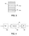
- decimating by M after the resampling merely consists of taking one out of every M samples since there is no replica of the signal to filter, in other words, there is no additional calculation. Furthermore, it is not necessary to calculate the samples that are eliminated, so the implementation of the resampling block (6), (16) or (23) can be simplified, as represented in figure 4 by means of the' block (15) which groups the resampler and the decimator. By simplifying the resampling filter, a more optimum solution can be obtained in terms of number of operations to perform by means of using this structure with interpolation and resampling than in the case of using a resampling structure directly.
Landscapes
- Engineering & Computer Science (AREA)
- Theoretical Computer Science (AREA)
- Computer Networks & Wireless Communication (AREA)
- Signal Processing (AREA)
- Transmission Systems Not Characterized By The Medium Used For Transmission (AREA)
- Analogue/Digital Conversion (AREA)
Applications Claiming Priority (2)
| Application Number | Priority Date | Filing Date | Title |
|---|---|---|---|
| ES200301288A ES2221570B2 (es) | 2003-05-30 | 2003-05-30 | Procedimiento de remuestreo en transmision y recepcion de una señal digital con traslacion en banda digital. |
| PCT/ES2004/000224 WO2004107584A1 (fr) | 2003-05-30 | 2004-05-31 | Procede de reechantillonnage dans la transmission et la reception d'un signal numerique avec translation dans la bande numerique |
Publications (2)
| Publication Number | Publication Date |
|---|---|
| EP1646151A1 true EP1646151A1 (fr) | 2006-04-12 |
| EP1646151B1 EP1646151B1 (fr) | 2018-07-11 |
Family
ID=33484262
Family Applications (1)
| Application Number | Title | Priority Date | Filing Date |
|---|---|---|---|
| EP04735485.7A Expired - Lifetime EP1646151B1 (fr) | 2003-05-30 | 2004-05-31 | Procede de reechantillonnage dans la transmission d'un signal numerique avec translation dans la bande numerique |
Country Status (14)
| Country | Link |
|---|---|
| US (1) | US20060120497A1 (fr) |
| EP (1) | EP1646151B1 (fr) |
| JP (1) | JP2006526345A (fr) |
| KR (1) | KR101078441B1 (fr) |
| CN (1) | CN100488055C (fr) |
| AU (1) | AU2004244394A1 (fr) |
| BR (1) | BRPI0410849A (fr) |
| CA (1) | CA2527649A1 (fr) |
| EA (1) | EA008651B1 (fr) |
| ES (1) | ES2221570B2 (fr) |
| IL (1) | IL172265A0 (fr) |
| MX (1) | MXPA05012861A (fr) |
| TW (1) | TWI254536B (fr) |
| WO (1) | WO2004107584A1 (fr) |
Cited By (2)
| Publication number | Priority date | Publication date | Assignee | Title |
|---|---|---|---|---|
| CN101114843B (zh) * | 2006-07-27 | 2011-06-01 | 索尼株式会社 | 接收装置以及接收方法 |
| CN101227256B (zh) * | 2006-10-12 | 2011-12-14 | 索尼株式会社 | 接收器设备、接收方法 |
Families Citing this family (7)
| Publication number | Priority date | Publication date | Assignee | Title |
|---|---|---|---|---|
| ES2221570B2 (es) | 2003-05-30 | 2005-10-01 | Diseño De Sistemas En Silicio, S.A. | Procedimiento de remuestreo en transmision y recepcion de una señal digital con traslacion en banda digital. |
| WO2008075268A1 (fr) * | 2006-12-19 | 2008-06-26 | Koninklijke Philips Electronics N.V. | Système d'irm avec récepteur numérique direct utilisant le re-échantillonnage |
| CN101867740B (zh) * | 2010-05-21 | 2013-06-19 | 深圳国微技术有限公司 | 用于数字电视基带信号的采样速率转换器及转换方法 |
| EP2630759B1 (fr) * | 2010-10-19 | 2019-03-20 | CommScope Technologies LLC | Procédés et dispositifs de transport de signaux rf numériques |
| US8724759B2 (en) * | 2011-05-06 | 2014-05-13 | I Berium Communications, Inc. | Coherent synchronization and framing in a digital television receiver |
| CN112350765B (zh) * | 2020-10-20 | 2022-03-22 | 中国电子科技集团公司第五十四研究所 | 一种基于数字重采样的多级全数字变频解调装置 |
| CN114785349B (zh) * | 2022-03-10 | 2025-04-11 | 安徽听见科技有限公司 | 一种信号采样同步方法、装置、设备及存储介质 |
Family Cites Families (16)
| Publication number | Priority date | Publication date | Assignee | Title |
|---|---|---|---|---|
| US4884265A (en) | 1987-04-30 | 1989-11-28 | Loral Corporation | Digital demodulator for frequency-division-multiplexed signals |
| US5365468A (en) * | 1992-02-17 | 1994-11-15 | Yamaha Corporation | Sampling frequency converter |
| GB9208493D0 (en) * | 1992-04-16 | 1992-06-03 | Thomson Consumer Electronics | Dual port video memory |
| US5495203A (en) * | 1994-12-02 | 1996-02-27 | Applied Signal Technology, Inc. | Efficient QAM equalizer/demodulator with non-integer sampling |
| US5748126A (en) * | 1996-03-08 | 1998-05-05 | S3 Incorporated | Sigma-delta digital-to-analog conversion system and process through reconstruction and resampling |
| US5818888A (en) * | 1997-02-26 | 1998-10-06 | Ericsson, Inc. | Sample rate converter |
| JP3836947B2 (ja) * | 1997-06-20 | 2006-10-25 | パイオニア株式会社 | サンプリングレート変換ユニット、サンプリングレート変換装置及びサンプリングレート変換方法 |
| US6411653B1 (en) * | 1999-07-16 | 2002-06-25 | Lucent Technologies Inc. | Cascaded polyphase DFT-filter band for a wireless telecommunications system |
| DE19960559A1 (de) * | 1999-12-15 | 2001-07-05 | Infineon Technologies Ag | Empfangsvorrichtung für winkelmodulierte Signale |
| SE519885C2 (sv) * | 2000-03-27 | 2003-04-22 | Ericsson Telefon Ab L M | Förfarande och anordning för omvandling av samplingsfrekvens |
| DE10036703B4 (de) * | 2000-07-27 | 2005-12-29 | Rohde & Schwarz Gmbh & Co. Kg | Verfahren und Vorrichtung zur Korrektur eines Resamplers |
| US6973146B1 (en) * | 2000-08-29 | 2005-12-06 | Lucent Technologies Inc. | Resampler for a bit pump and method of resampling a signal associated therewith |
| ES2188370B1 (es) * | 2001-05-21 | 2004-10-16 | Diseño De Sistemas En Silicio, S.A. | Procedimiento para la sincronizacion en el enlace descendente de multiples usuarios en un sistema de transmision punto a multipunto con modulacion ofdm. |
| DE10133898C1 (de) * | 2001-07-12 | 2002-10-17 | Infineon Technologies Ag | Empfänger mit einem integrierten Taktphasendetektor |
| US7072418B2 (en) * | 2001-09-18 | 2006-07-04 | Thomson Licensing | Method and apparatus for performing Nyquist folding frequency modulation |
| ES2221570B2 (es) | 2003-05-30 | 2005-10-01 | Diseño De Sistemas En Silicio, S.A. | Procedimiento de remuestreo en transmision y recepcion de una señal digital con traslacion en banda digital. |
-
2003
- 2003-05-30 ES ES200301288A patent/ES2221570B2/es not_active Expired - Fee Related
-
2004
- 2004-05-31 MX MXPA05012861A patent/MXPA05012861A/es active IP Right Grant
- 2004-05-31 BR BRPI0410849-3A patent/BRPI0410849A/pt not_active IP Right Cessation
- 2004-05-31 WO PCT/ES2004/000224 patent/WO2004107584A1/fr not_active Ceased
- 2004-05-31 EP EP04735485.7A patent/EP1646151B1/fr not_active Expired - Lifetime
- 2004-05-31 CN CNB2004800221390A patent/CN100488055C/zh not_active Expired - Lifetime
- 2004-05-31 EA EA200501938A patent/EA008651B1/ru not_active IP Right Cessation
- 2004-05-31 CA CA002527649A patent/CA2527649A1/fr not_active Abandoned
- 2004-05-31 TW TW093115633A patent/TWI254536B/zh not_active IP Right Cessation
- 2004-05-31 AU AU2004244394A patent/AU2004244394A1/en not_active Abandoned
- 2004-05-31 KR KR1020057022978A patent/KR101078441B1/ko not_active Expired - Fee Related
- 2004-05-31 JP JP2006508324A patent/JP2006526345A/ja active Pending
-
2005
- 2005-11-29 US US11/288,957 patent/US20060120497A1/en not_active Abandoned
- 2005-11-29 IL IL172265A patent/IL172265A0/en unknown
Non-Patent Citations (1)
| Title |
|---|
| See references of WO2004107584A1 * |
Cited By (2)
| Publication number | Priority date | Publication date | Assignee | Title |
|---|---|---|---|---|
| CN101114843B (zh) * | 2006-07-27 | 2011-06-01 | 索尼株式会社 | 接收装置以及接收方法 |
| CN101227256B (zh) * | 2006-10-12 | 2011-12-14 | 索尼株式会社 | 接收器设备、接收方法 |
Also Published As
| Publication number | Publication date |
|---|---|
| MXPA05012861A (es) | 2006-02-22 |
| WO2004107584A1 (fr) | 2004-12-09 |
| CN1830147A (zh) | 2006-09-06 |
| CN100488055C (zh) | 2009-05-13 |
| TWI254536B (en) | 2006-05-01 |
| KR101078441B1 (ko) | 2011-11-01 |
| EP1646151B1 (fr) | 2018-07-11 |
| EA008651B1 (ru) | 2007-06-29 |
| IL172265A0 (en) | 2006-04-10 |
| KR20060041174A (ko) | 2006-05-11 |
| JP2006526345A (ja) | 2006-11-16 |
| EA200501938A1 (ru) | 2006-06-30 |
| TW200501685A (en) | 2005-01-01 |
| BRPI0410849A (pt) | 2006-07-04 |
| CA2527649A1 (fr) | 2004-12-09 |
| ES2221570B2 (es) | 2005-10-01 |
| ES2221570A1 (es) | 2004-12-16 |
| US20060120497A1 (en) | 2006-06-08 |
| AU2004244394A1 (en) | 2004-12-09 |
Similar Documents
| Publication | Publication Date | Title |
|---|---|---|
| US6539052B1 (en) | System for accelerating the reconfiguration of a transceiver and method therefor | |
| US5612975A (en) | Digital receiver for variable data rate communications | |
| CA2681362C (fr) | Extremite frontale d'emetteur-recepteur pour des systemes de radio logicielle | |
| CN106972832B (zh) | 一种可任意倍数重采样的数字下变频器 | |
| US5933452A (en) | Timing interpolator in digital demodulator | |
| JP3986891B2 (ja) | デジタル通信受信機における受信信号のデジタル復調装置および方法 | |
| CN111194077A (zh) | 一种低采样率下的定时同步方法 | |
| EP1646151A1 (fr) | Procede de reechantillonnage dans la transmission et la reception d'un signal numerique avec translation dans la bande numerique | |
| EP1192723A1 (fr) | Emetteur-recepteur fi numerique programmable | |
| US5970086A (en) | Radio remote interface for modulating/demodulating data in a digital communication system | |
| CN111683028B (zh) | 一种数字等报幅cw信号解调方法 | |
| HK1090473A (en) | Method for resampling at transmission and reception of a digital signal with digital band translation | |
| JP3986890B2 (ja) | デジタル通信受信機における受信信号のデジタル復調装置および方法 | |
| EP1693954B1 (fr) | Circuit de démodulation pour un récepteur employant un schéma d'échantillonnage FI | |
| JP2002300224A (ja) | 受信装置 | |
| JP2001268066A (ja) | 同期検出装置及び同期検出方法 | |
| JP3893197B2 (ja) | デジタル変調回路 | |
| Sinha et al. | Digital Front End in Software Defined Radio | |
| KR940027326A (ko) | 디지탈 심볼 동기 장치 및 방법 | |
| Li | A DSP-Based it/4-DQPSK Modem | |
| HK1058864B (en) | Apparatus and method for encoding of information and apparatus and method for decoding of encoded information |
Legal Events
| Date | Code | Title | Description |
|---|---|---|---|
| PUAI | Public reference made under article 153(3) epc to a published international application that has entered the european phase |
Free format text: ORIGINAL CODE: 0009012 |
|
| 17P | Request for examination filed |
Effective date: 20051230 |
|
| AK | Designated contracting states |
Kind code of ref document: A1 Designated state(s): AT BE BG CH CY CZ DE DK EE ES FI FR GB GR HU IE IT LI LU MC NL PL PT RO SE SI SK TR |
|
| DAX | Request for extension of the european patent (deleted) | ||
| REG | Reference to a national code |
Ref country code: HK Ref legal event code: DE Ref document number: 1090473 Country of ref document: HK |
|
| RIN1 | Information on inventor provided before grant (corrected) |
Inventor name: GARC A SAN JOS , AITOR Inventor name: BLASCO CLARET, JORGE VICENTE Inventor name: RIVEIRO INSUA, JUAN CARLOS Inventor name: IRANZO MOLINERO, SALVADOR |
|
| RAP1 | Party data changed (applicant data changed or rights of an application transferred) |
Owner name: MARVELL HISPANIA S.L. |
|
| REG | Reference to a national code |
Ref country code: HK Ref legal event code: WD Ref document number: 1090473 Country of ref document: HK |
|
| 17Q | First examination report despatched |
Effective date: 20130219 |
|
| REG | Reference to a national code |
Ref country code: DE Ref legal event code: R079 Ref document number: 602004052918 Country of ref document: DE Free format text: PREVIOUS MAIN CLASS: H03M0007000000 Ipc: H03M0001080000 |
|
| RIC1 | Information provided on ipc code assigned before grant |
Ipc: H03M 3/00 20060101ALI20171201BHEP Ipc: H03M 1/08 20060101AFI20171201BHEP Ipc: H03M 1/66 20060101ALI20171201BHEP Ipc: H03M 1/12 20060101ALI20171201BHEP |
|
| GRAP | Despatch of communication of intention to grant a patent |
Free format text: ORIGINAL CODE: EPIDOSNIGR1 |
|
| STAA | Information on the status of an ep patent application or granted ep patent |
Free format text: STATUS: GRANT OF PATENT IS INTENDED |
|
| INTG | Intention to grant announced |
Effective date: 20180129 |
|
| RIN1 | Information on inventor provided before grant (corrected) |
Inventor name: BLASCO CLARET, JORGE VICENTE Inventor name: GARCIA SAN JOSE , AITOR Inventor name: RIVEIRO INSUA, JUAN CARLOS Inventor name: IRANZO MOLINERO, SALVADOR |
|
| GRAS | Grant fee paid |
Free format text: ORIGINAL CODE: EPIDOSNIGR3 |
|
| GRAA | (expected) grant |
Free format text: ORIGINAL CODE: 0009210 |
|
| STAA | Information on the status of an ep patent application or granted ep patent |
Free format text: STATUS: THE PATENT HAS BEEN GRANTED |
|
| AK | Designated contracting states |
Kind code of ref document: B1 Designated state(s): AT BE BG CH CY CZ DE DK EE ES FI FR GB GR HU IE IT LI LU MC NL PL PT RO SE SI SK TR |
|
| REG | Reference to a national code |
Ref country code: GB Ref legal event code: FG4D |
|
| REG | Reference to a national code |
Ref country code: CH Ref legal event code: EP |
|
| REG | Reference to a national code |
Ref country code: AT Ref legal event code: REF Ref document number: 1017973 Country of ref document: AT Kind code of ref document: T Effective date: 20180715 |
|
| REG | Reference to a national code |
Ref country code: DE Ref legal event code: R096 Ref document number: 602004052918 Country of ref document: DE |
|
| REG | Reference to a national code |
Ref country code: IE Ref legal event code: FG4D |
|
| REG | Reference to a national code |
Ref country code: NL Ref legal event code: MP Effective date: 20180711 |
|
| REG | Reference to a national code |
Ref country code: AT Ref legal event code: MK05 Ref document number: 1017973 Country of ref document: AT Kind code of ref document: T Effective date: 20180711 |
|
| PG25 | Lapsed in a contracting state [announced via postgrant information from national office to epo] |
Ref country code: NL Free format text: LAPSE BECAUSE OF FAILURE TO SUBMIT A TRANSLATION OF THE DESCRIPTION OR TO PAY THE FEE WITHIN THE PRESCRIBED TIME-LIMIT Effective date: 20180711 |
|
| PG25 | Lapsed in a contracting state [announced via postgrant information from national office to epo] |
Ref country code: GR Free format text: LAPSE BECAUSE OF FAILURE TO SUBMIT A TRANSLATION OF THE DESCRIPTION OR TO PAY THE FEE WITHIN THE PRESCRIBED TIME-LIMIT Effective date: 20181012 Ref country code: AT Free format text: LAPSE BECAUSE OF FAILURE TO SUBMIT A TRANSLATION OF THE DESCRIPTION OR TO PAY THE FEE WITHIN THE PRESCRIBED TIME-LIMIT Effective date: 20180711 Ref country code: PL Free format text: LAPSE BECAUSE OF FAILURE TO SUBMIT A TRANSLATION OF THE DESCRIPTION OR TO PAY THE FEE WITHIN THE PRESCRIBED TIME-LIMIT Effective date: 20180711 Ref country code: SE Free format text: LAPSE BECAUSE OF FAILURE TO SUBMIT A TRANSLATION OF THE DESCRIPTION OR TO PAY THE FEE WITHIN THE PRESCRIBED TIME-LIMIT Effective date: 20180711 Ref country code: FI Free format text: LAPSE BECAUSE OF FAILURE TO SUBMIT A TRANSLATION OF THE DESCRIPTION OR TO PAY THE FEE WITHIN THE PRESCRIBED TIME-LIMIT Effective date: 20180711 Ref country code: BG Free format text: LAPSE BECAUSE OF FAILURE TO SUBMIT A TRANSLATION OF THE DESCRIPTION OR TO PAY THE FEE WITHIN THE PRESCRIBED TIME-LIMIT Effective date: 20181011 |
|
| PG25 | Lapsed in a contracting state [announced via postgrant information from national office to epo] |
Ref country code: ES Free format text: LAPSE BECAUSE OF FAILURE TO SUBMIT A TRANSLATION OF THE DESCRIPTION OR TO PAY THE FEE WITHIN THE PRESCRIBED TIME-LIMIT Effective date: 20180711 |
|
| REG | Reference to a national code |
Ref country code: DE Ref legal event code: R097 Ref document number: 602004052918 Country of ref document: DE |
|
| PG25 | Lapsed in a contracting state [announced via postgrant information from national office to epo] |
Ref country code: EE Free format text: LAPSE BECAUSE OF FAILURE TO SUBMIT A TRANSLATION OF THE DESCRIPTION OR TO PAY THE FEE WITHIN THE PRESCRIBED TIME-LIMIT Effective date: 20180711 Ref country code: CZ Free format text: LAPSE BECAUSE OF FAILURE TO SUBMIT A TRANSLATION OF THE DESCRIPTION OR TO PAY THE FEE WITHIN THE PRESCRIBED TIME-LIMIT Effective date: 20180711 Ref country code: RO Free format text: LAPSE BECAUSE OF FAILURE TO SUBMIT A TRANSLATION OF THE DESCRIPTION OR TO PAY THE FEE WITHIN THE PRESCRIBED TIME-LIMIT Effective date: 20180711 Ref country code: IT Free format text: LAPSE BECAUSE OF FAILURE TO SUBMIT A TRANSLATION OF THE DESCRIPTION OR TO PAY THE FEE WITHIN THE PRESCRIBED TIME-LIMIT Effective date: 20180711 |
|
| PLBE | No opposition filed within time limit |
Free format text: ORIGINAL CODE: 0009261 |
|
| STAA | Information on the status of an ep patent application or granted ep patent |
Free format text: STATUS: NO OPPOSITION FILED WITHIN TIME LIMIT |
|
| PG25 | Lapsed in a contracting state [announced via postgrant information from national office to epo] |
Ref country code: SK Free format text: LAPSE BECAUSE OF FAILURE TO SUBMIT A TRANSLATION OF THE DESCRIPTION OR TO PAY THE FEE WITHIN THE PRESCRIBED TIME-LIMIT Effective date: 20180711 Ref country code: DK Free format text: LAPSE BECAUSE OF FAILURE TO SUBMIT A TRANSLATION OF THE DESCRIPTION OR TO PAY THE FEE WITHIN THE PRESCRIBED TIME-LIMIT Effective date: 20180711 |
|
| 26N | No opposition filed |
Effective date: 20190412 |
|
| PG25 | Lapsed in a contracting state [announced via postgrant information from national office to epo] |
Ref country code: SI Free format text: LAPSE BECAUSE OF FAILURE TO SUBMIT A TRANSLATION OF THE DESCRIPTION OR TO PAY THE FEE WITHIN THE PRESCRIBED TIME-LIMIT Effective date: 20180711 |
|
| REG | Reference to a national code |
Ref country code: CH Ref legal event code: PL |
|
| GBPC | Gb: european patent ceased through non-payment of renewal fee |
Effective date: 20190531 |
|
| PG25 | Lapsed in a contracting state [announced via postgrant information from national office to epo] |
Ref country code: CH Free format text: LAPSE BECAUSE OF NON-PAYMENT OF DUE FEES Effective date: 20190531 Ref country code: MC Free format text: LAPSE BECAUSE OF FAILURE TO SUBMIT A TRANSLATION OF THE DESCRIPTION OR TO PAY THE FEE WITHIN THE PRESCRIBED TIME-LIMIT Effective date: 20180711 Ref country code: LI Free format text: LAPSE BECAUSE OF NON-PAYMENT OF DUE FEES Effective date: 20190531 |
|
| REG | Reference to a national code |
Ref country code: BE Ref legal event code: MM Effective date: 20190531 |
|
| PG25 | Lapsed in a contracting state [announced via postgrant information from national office to epo] |
Ref country code: LU Free format text: LAPSE BECAUSE OF NON-PAYMENT OF DUE FEES Effective date: 20190531 |
|
| PG25 | Lapsed in a contracting state [announced via postgrant information from national office to epo] |
Ref country code: TR Free format text: LAPSE BECAUSE OF FAILURE TO SUBMIT A TRANSLATION OF THE DESCRIPTION OR TO PAY THE FEE WITHIN THE PRESCRIBED TIME-LIMIT Effective date: 20180711 |
|
| PG25 | Lapsed in a contracting state [announced via postgrant information from national office to epo] |
Ref country code: IE Free format text: LAPSE BECAUSE OF NON-PAYMENT OF DUE FEES Effective date: 20190531 Ref country code: GB Free format text: LAPSE BECAUSE OF NON-PAYMENT OF DUE FEES Effective date: 20190531 |
|
| PG25 | Lapsed in a contracting state [announced via postgrant information from national office to epo] |
Ref country code: BE Free format text: LAPSE BECAUSE OF NON-PAYMENT OF DUE FEES Effective date: 20190531 |
|
| PG25 | Lapsed in a contracting state [announced via postgrant information from national office to epo] |
Ref country code: PT Free format text: LAPSE BECAUSE OF FAILURE TO SUBMIT A TRANSLATION OF THE DESCRIPTION OR TO PAY THE FEE WITHIN THE PRESCRIBED TIME-LIMIT Effective date: 20181111 Ref country code: FR Free format text: LAPSE BECAUSE OF NON-PAYMENT OF DUE FEES Effective date: 20190531 |
|
| PG25 | Lapsed in a contracting state [announced via postgrant information from national office to epo] |
Ref country code: CY Free format text: LAPSE BECAUSE OF FAILURE TO SUBMIT A TRANSLATION OF THE DESCRIPTION OR TO PAY THE FEE WITHIN THE PRESCRIBED TIME-LIMIT Effective date: 20180711 |
|
| PG25 | Lapsed in a contracting state [announced via postgrant information from national office to epo] |
Ref country code: HU Free format text: LAPSE BECAUSE OF FAILURE TO SUBMIT A TRANSLATION OF THE DESCRIPTION OR TO PAY THE FEE WITHIN THE PRESCRIBED TIME-LIMIT; INVALID AB INITIO Effective date: 20040531 |
|
| PGFP | Annual fee paid to national office [announced via postgrant information from national office to epo] |
Ref country code: DE Payment date: 20230530 Year of fee payment: 20 |
|
| REG | Reference to a national code |
Ref country code: DE Ref legal event code: R071 Ref document number: 602004052918 Country of ref document: DE |