EP1646883B1 - Ic mit eingebauter karakteristikbestimmung - Google Patents
Ic mit eingebauter karakteristikbestimmung Download PDFInfo
- Publication number
- EP1646883B1 EP1646883B1 EP04744458A EP04744458A EP1646883B1 EP 1646883 B1 EP1646883 B1 EP 1646883B1 EP 04744458 A EP04744458 A EP 04744458A EP 04744458 A EP04744458 A EP 04744458A EP 1646883 B1 EP1646883 B1 EP 1646883B1
- Authority
- EP
- European Patent Office
- Prior art keywords
- operable
- semiconductor device
- test
- characterization
- data
- Prior art date
- Legal status (The legal status is an assumption and is not a legal conclusion. Google has not performed a legal analysis and makes no representation as to the accuracy of the status listed.)
- Expired - Lifetime
Links
Images


Classifications
-
- G—PHYSICS
- G01—MEASURING; TESTING
- G01R—MEASURING ELECTRIC VARIABLES; MEASURING MAGNETIC VARIABLES
- G01R31/00—Arrangements for testing electric properties; Arrangements for locating electric faults; Arrangements for electrical testing characterised by what is being tested not provided for elsewhere
- G01R31/28—Testing of electronic circuits, e.g. by signal tracer
- G01R31/317—Testing of digital circuits
- G01R31/3181—Functional testing
- G01R31/3187—Built-in tests
-
- H—ELECTRICITY
- H10—SEMICONDUCTOR DEVICES; ELECTRIC SOLID-STATE DEVICES NOT OTHERWISE PROVIDED FOR
- H10P—GENERIC PROCESSES OR APPARATUS FOR THE MANUFACTURE OR TREATMENT OF DEVICES COVERED BY CLASS H10
- H10P74/00—Testing or measuring during manufacture or treatment of wafers, substrates or devices
-
- G—PHYSICS
- G01—MEASURING; TESTING
- G01R—MEASURING ELECTRIC VARIABLES; MEASURING MAGNETIC VARIABLES
- G01R31/00—Arrangements for testing electric properties; Arrangements for locating electric faults; Arrangements for electrical testing characterised by what is being tested not provided for elsewhere
- G01R31/28—Testing of electronic circuits, e.g. by signal tracer
- G01R31/317—Testing of digital circuits
- G01R31/3181—Functional testing
- G01R31/319—Tester hardware, i.e. output processing circuits
- G01R31/31903—Tester hardware, i.e. output processing circuits tester configuration
- G01R31/31915—In-circuit Testers
-
- H—ELECTRICITY
- H10—SEMICONDUCTOR DEVICES; ELECTRIC SOLID-STATE DEVICES NOT OTHERWISE PROVIDED FOR
- H10P—GENERIC PROCESSES OR APPARATUS FOR THE MANUFACTURE OR TREATMENT OF DEVICES COVERED BY CLASS H10
- H10P95/00—Generic processes or apparatus for manufacture or treatments not covered by the other groups of this subclass
Definitions
- the present invention relates to the field of integrated circuit (IC) testing.
- an IC is tested to ensure its quality and functionality. If, at any point during the production cycle, an IC is found not to function correctly, or has operating parameters which fall outside specified ranges, it may be discarded in order to save time and money.
- tests to determine functionality are also performed in order to ascertain certain operating parameters of an IC such as maximum and minimum operating voltage and/or temperature, and maximum and minimum applicable clock frequencies, for example.
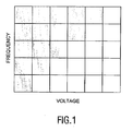
- Figure 1 shows the results of a typical characterization process carried out using expensive test equipment.
- Figure 1 is a so-called ⁇ Shmoo plot', which shows a characterization of the frequency of an IC versus supply voltage of the IC in question.
- a Shmoo plot is a graph which represents how a particular test passes or fails when parameters like frequency, voltage, or temperature are varied and the test is executed repeatedly on the IC in question.
- the shape of the failing region is meaningful and helps in determining the cause of the failure.
- a pass is shown as a white square
- a fail is shown as a grey square.
- a Shmoo plot of a normal circuit operation shows better high-frequency performance as supply voltage increases, as shown in figure 1.
- characterization tests In order to make characterization tests viable, they must be performed quickly, and utilize as little test equipment as possible. However, as mentioned, due to increasing process shifts (even on a single wafer) for new semiconductor IC technologies, a characterization test is unlikely to produce the same results (i.e. operating parameters) for every IC. However, in order to ensure low production costs, it is not practicable to separately characterize every IC at the end of its production process using the test equipment.
- US 6,556,938 discloses a system for facilitating automated test equipment functionality within integrated circuits.
- the integrated circuit comprises a parametric test circuit that is adapted to electrically communicate with automated test equipment, so that in response to a signal received from the automated test equipment, the parametric test circuit measures at least one parameter of a first pad of the integrated circuit.
- a semiconductor device comprising a functional device and a characterization unit, characterized in that the characterization unit is operable to control the variation of an operating parameter of the device to provide characterization data for the device with respect to the varied operating parameter.
- a method of characterizing a semiconductor device comprising a functional device and a characterization unit, characterized in that the method comprises:
- Figure 2 shows an IC 201 having an architecture according to an aspect of the present invention.
- a supply voltage and clock signal of the IC 201 are controlled by a voltage controller 203, and a clock controller 205 respectively.
- the voltage controller 203 is operable to provide a variable voltage supply to a device under characterization (DUC) 207
- the clock controller 205 is operable to provide a variable clock signal to the DUC 207 (i.e. a clock signal with a variable period).
- the controllers 203, 205 may usefully be described as 'characterization parameter controllers' to describe their function as controllers which are operable to control a characterization parameter of the DUC 207.
- a test interface is provided in order to supply instructions to the controllers 203, 205.
- a hardware or software controller is available outside of the IC 201 in order to execute a characterization.
- Test stimuli are applied to the DUC 207 externally through an interface.
- the clock controller 205 is also operable to output the clock signal from the IC 201 in order to synchronize the test stimuli and responses thereto to the external world.
- the implementation of the system of figure 2 requires a test interface which is operable to provide the voltage controller 203 and the clock controller 205 with the required parameters in order to start a characterization process.
- the DUC 207 is provided with the test stimuli from an external hardware or software source through a further interface.
- the DUC 207 provides the functionality of the IC 201, and all other parts of the IC 201 such as the voltage controller 203 and the clock controller 205 are ancillary items providing test functionality on the IC 201 in accordance with the present invention.
- the parameters used to perform the characterization are therefore voltage and clock period. It will appreciated, however, that any parameter suitable for forming a characterization of a DUC 207 may be controlled by the controllers 203, 205.
- IC characterization may be performed 'on-chip', thereby providing a built-in chip characterization (BICC) system.
- BICC built-in chip characterization
- FIG. 3 shows an IC 301 having an architecture according to a second embodiment of the present invention.
- a device under characterization 303 (DUC) is surrounded by built-in self test (BIST) hardware 305 that is operable to generate test stimuli and observe the responses.
- BIST built-in self test
- a supply voltage and clock signal of the IC 301 are controlled by a voltage controller 307, and a clock controller 309.
- voltage controller 307 is operable to provide a variable voltage supply to both the DUC 303, and the BIST hardware 305
- the clock controller 309 is operable to provide a variable clock signal to the DUC 303.
- the clock signal is also supplied to the BIST hardware 305.
- Both the controllers 307, 309 are controlled by the use of external software or hardware control means (not shown).
- the controllers 307, 309 receive data through a test interface of IC 301.
- the DUC 303 provides the functionality of the IC 301, and all other parts of the IC 301 such as the BIST hardware 305, the voltage controller 307 and clock controller 309, are ancillary items providing test functionality on the IC 301.
- test stimuli are generated internally via the BIST module 309.
- the test results are output through the test interface.
- the controllers 307, 309 are operable to vary a characterization parameter of the DUC 303.
- a test is performed on the DUC 303.
- characterization of the DUC 303 is performed, the results of which are output from the IC as explained above.
- the results may be used to generate a Shmoo plot similar to that shown in figure 1, so as to provide a characterization of the DUC 303 with respect to the parameters controlled by controllers 307, 309 (i.e. voltage and clock period respectively in the example of figure 3).
- FIG. 2 The implementations of figures 2 and 3 provide BICC functionality, but requires the use of an external (to the IC 201, 301) software or hardware. In this way, IC area may be saved as an internal global control module is not required.
- FIG. 4 shows an IC 401 according to another embodiment of the present invention.
- the BICC system comprises a voltage controller 403, a clock controller 405, a DUC 407, and BIST functionality provided by BIST hardware 409, similar to that shown in figure 3.
- a test interface is provided in order to supply instructions to a global controller 411.
- the global controller 411 receives a prompt through the test interface in order to start a characterization process.
- the prompt can include a request to the global controller 411 to begin the process, and can also include the parameters of the chip 401 that are to be characterized during the process.
- the controller 411 Upon reception of this prompt data, the controller 411 is operable to vary certain parameters of the chip 401 via the use of the controllers 403, 405 (which in this case control a voltage and clock signal respectively).
- the global controller 411 after having received the necessary prompt and characterization parameters through the test interface, is operable to vary certain parameters of the DUC 407 via the use of the controllers 403, 405.
- controllers 403, 405 control a voltage and clock signal of the DUC 407 respectively, and will therefore enable a characterization of the DUC 407 to be performed with respect to IC supply voltage and clock frequency.
- Such a characterization is usefully depicted in the form of a Shmoo plot as described above with reference to figure 1.
- the global controller 411 is operable to program the controllers 403, 405 repeatedly so that a 'virtual' Shmoo plot may be generated.
- the Shmoo plot will only have pass/fail information. If, however, no BIST is used (figure 2), the Shmoo plot may also contain the number of faults per test. In general, however, the virtual Shmoo plots as generated by the characterization process of the present invention are the same as those generated using external test equipment. As is necessary for Shmoo plots generated by the test equipment, external software is required in order to be able to view and evaluate the Shmoo plots.
- any suitable parameter of the DUC 403 may be controlled by controllers 403, 405.
- controllers 403, 405. The use of voltage and clock controllers is not intended to be limiting, and is merely included in order to better explain the inventive concept and particular advantages brought forth by the present invention.
- characterization information is output directly via the test interface.
Landscapes
- Engineering & Computer Science (AREA)
- General Engineering & Computer Science (AREA)
- Physics & Mathematics (AREA)
- General Physics & Mathematics (AREA)
- Semiconductor Integrated Circuits (AREA)
- Tests Of Electronic Circuits (AREA)
- Heterocyclic Carbon Compounds Containing A Hetero Ring Having Oxygen Or Sulfur (AREA)
- Testing Or Measuring Of Semiconductors Or The Like (AREA)
Claims (24)
- Halbleiteranordnung (201) mit einer Funktionsanordnung (207) und einer Charakterisierungseinheit (203),
dadurch gekennzeichnet, dass die Charakterisierungseinheit wirksam ist, die Variation eines Arbeitsparameters der Anordnung zu steuern, um die Charakterisierungsdaten für die Anordnung (201) in Bezug auf den variierten Arbeitsparameter zur Verfügung zu stellen. - Halbleiteranordnung (201) nach Anspruch 1, dadurch gekennzeichnet, dass die Charakterisierungseinheit (203) wirksam ist, ein Steuersignal zum Steuern eines Arbeitsparameters der Anordnung (201) zu liefern.
- Halbleiteranordnung (201) nach Anspruch 2, dadurch gekennzeichnet, dass die integrierte Charakterisierungseinheit (203) wirksam ist, ein Steuersignal zum Steuern einer Spannungsversorgung der Anordnung (201) zu steuern.
- Halbleiteranordnung (201) nach Anspruch 2 oder 3, dadurch gekennzeichnet, dass die integrierte Charakterisierungseinheit (203) wirksam ist, ein Steuersignal zum Steuern eines Taktsignals der Anordnung (201) zu steuern.
- Halbleiteranordnung (201) nach einem oder mehreren der Ansprüche 1 bis 4, dadurch gekennzeichnet, dass die Funktionsanordnung (207) wirksam ist, Testdaten zu empfangen.
- Halbleiteranordnung (201) nach Anspruch 5, dadurch gekennzeichnet, dass die Funktionsanordnung (207) wirksam ist, abhängig von den Testdaten eine Testreaktion zu produzieren.
- Halbleiteranordnung (201) nach Anspruch 5 oder 6, dadurch gekennzeichnet, dass die Funktionsanordnung (207) wirksam ist, ein Steuersignal von der Charakterisierungseinheit (207) zu empfangen.
- Halbleiteranordnung (201) nach Anspruch 4, dadurch gekennzeichnet, dass die Charakterisierungseinheit (203) wirksam ist, der Anordnung (201) das Taktsignal extern zuzuführen.
- Halbleiteranordnung (201) nach einem oder mehreren der vorstehenden Ansprüche, dadurch gekennzeichnet, dass eine Test-Schnittstelle vorgesehen ist und dass die Charakterisierungseinheit (207) wirksam ist, Daten über die Test-Schnittstelle zu empfangen.
- Halbleiteranordnung (201) nach einem oder mehreren der vorstehenden Ansprüche, dadurch gekennzeichnet, dass Software-Steuermittel vorgesehen sind, die wirksam sind, Steuerdaten an die Charakterisierungseinheit (207) zu liefern.
- Halbleiteranordnung (201) nach einem oder mehreren der vorstehenden Ansprüche, dadurch gekennzeichnet, dass Hardware-Steuermittel vorgesehen sind, die wirksam sind, Steuerdaten an die Charakterisierungseinheit (207) zu liefern.
- Halbleiteranordnung (201) nach Anspruch 10 oder 11, dadurch gekennzeichnet, dass die Steuermittel wirksam sind, Steuerdaten an die Charakterisierungseinheit (207) über die Test-Schnittstelle der Anordnung (201) zu liefern.
- Halbleiteranordnung (301) nach Anspruch 5, dadurch gekennzeichnet, dass eine eingebaute Testhardware (305) vorgesehen ist, die wirksam ist, Testdaten an die Funktionsanordnung (303) zu liefern.
- Halbleiteranordnung (301) nach Anspruch 13, dadurch gekennzeichnet, dass die eingebaute Testhardware (305) mit der IEEE 1149.1 konform ist.
- Halbleiteranordnung (301) nach Anspruch 13 oder 14, dadurch gekennzeichnet, dass eine Test-Schnittstelle vorgesehen ist und dass die eingebaute Testhardware (305) wirksam ist, Testdaten über eine Test-Schnittstelle der Anordnung (301) zu empfangen.
- Halbleiteranordnung (301) nach Anspruch 13 bis 15, dadurch gekennzeichnet, dass die eingebaute Testhardware (305) wirksam ist, abhängig von den der Funktionsanordnung (303) zugeführten Testdaten Testreaktionsdaten zu liefern.
- Halbleiteranordnung (301) nach Anspruch 16, dadurch gekennzeichnet, dass die eingebaute Testhardware (305) wirksam ist, aus der Anordnung (301) Testreaktionsdaten auszugeben.
- Halbleiteranordnung (401) nach einem oder mehreren der vorstehenden Ansprüche, dadurch gekennzeichnet, dass ein Speichermodul (413) vorgesehen ist, das wirksam ist, Charakterisierungsdaten der Anordnung (401) zu speichern.
- Halbleiteranordnung (401) nach einem oder mehreren der vorstehenden Ansprüche, dadurch gekennzeichnet, dass eine Steuereinheit (411) vorgesehen ist, die wirksam ist, Steuerdaten an die Charakterisierungseinheit (407) zu liefern.
- Halbleiteranordnung (401) nach Anspruch 19, wenn abhängig vom Anspruch 13, dadurch gekennzeichnet, dass die Steuereinheit (411) wirksam ist, Steuerdaten an die eingebaute Testhardware zu liefern.
- Halbleiteranordnung (401) nach Anspruch 19, wenn abhängig vom Anspruch 18, dadurch gekennzeichnet, dass die Steuereinheit (411) wirksam ist, mit dem Speichermodul (413) zu kommunizieren.
- Halbleiteranordnung (401) nach Anspruch 19, dadurch gekennzeichnet, dass die Steuereinheit (411) wirksam ist, Daten über eine Test-Schnittstelle der Anordnung (401) zu empfangen.
- Verfahren zum Kennzeichnen einer Halbleiteranordnung (201), bei dem die Halbleiteranordnung eine Funktionsanordnung (207) und eine Charakterisierungseinheit (203) aufweist, und bei dem das Verfahren gekennzeichnet ist durch- Variieren eines Arbeitsparameters der Anordnung unter Steuerung durch die Charakterisierungseinheit, und- Erreichen von Charakterisierungsdaten in Bezug auf den variierenden Arbeitsparameter von der Charakterisierungseinheit (203).
- Verfahren nach Anspruch 23, dadurch gekennzeichnet, dass die Charakterisierungseinheit ein Steuersignal zum Steuern eines Arbeitsparameters der Anordnung (201) liefert.
Priority Applications (1)
| Application Number | Priority Date | Filing Date | Title |
|---|---|---|---|
| EP04744458A EP1646883B8 (de) | 2003-07-09 | 2004-07-01 | Ic mit eingebauter karakteristikbestimmung |
Applications Claiming Priority (3)
| Application Number | Priority Date | Filing Date | Title |
|---|---|---|---|
| EP03102062 | 2003-07-09 | ||
| EP04744458A EP1646883B8 (de) | 2003-07-09 | 2004-07-01 | Ic mit eingebauter karakteristikbestimmung |
| PCT/IB2004/051089 WO2005006005A1 (en) | 2003-07-09 | 2004-07-01 | Ic with on-board characterization unit |
Publications (3)
| Publication Number | Publication Date |
|---|---|
| EP1646883A1 EP1646883A1 (de) | 2006-04-19 |
| EP1646883B1 true EP1646883B1 (de) | 2007-07-11 |
| EP1646883B8 EP1646883B8 (de) | 2007-09-05 |
Family
ID=34042919
Family Applications (1)
| Application Number | Title | Priority Date | Filing Date |
|---|---|---|---|
| EP04744458A Expired - Lifetime EP1646883B8 (de) | 2003-07-09 | 2004-07-01 | Ic mit eingebauter karakteristikbestimmung |
Country Status (9)
| Country | Link |
|---|---|
| US (1) | US7475312B2 (de) |
| EP (1) | EP1646883B8 (de) |
| JP (1) | JP2007527110A (de) |
| KR (1) | KR20060028810A (de) |
| CN (1) | CN100592097C (de) |
| AT (1) | ATE366941T1 (de) |
| DE (1) | DE602004007525T2 (de) |
| TW (1) | TW200508632A (de) |
| WO (1) | WO2005006005A1 (de) |
Families Citing this family (4)
| Publication number | Priority date | Publication date | Assignee | Title |
|---|---|---|---|---|
| US8484524B2 (en) * | 2007-08-21 | 2013-07-09 | Qualcomm Incorporated | Integrated circuit with self-test feature for validating functionality of external interfaces |
| US10768230B2 (en) * | 2016-05-27 | 2020-09-08 | International Business Machines Corporation | Built-in device testing of integrated circuits |
| US10685730B1 (en) * | 2018-03-20 | 2020-06-16 | Seagate Technology Llc | Circuit including efficient clocking for testing memory interface |
| CN113242976B (zh) | 2018-10-01 | 2024-09-17 | 大众汽车股份公司 | 用于监测电子系统的可靠性的方法和装置 |
Family Cites Families (17)
| Publication number | Priority date | Publication date | Assignee | Title |
|---|---|---|---|---|
| US7137048B2 (en) * | 2001-02-02 | 2006-11-14 | Rambus Inc. | Method and apparatus for evaluating and optimizing a signaling system |
| JPH04212524A (ja) * | 1990-12-06 | 1992-08-04 | Matsushita Electric Ind Co Ltd | 半導体集積回路 |
| CN1032983C (zh) * | 1991-01-26 | 1996-10-09 | 中国科学院广州电子技术研究所 | 半导体器件特性测试装置 |
| US6466520B1 (en) * | 1996-09-17 | 2002-10-15 | Xilinx, Inc. | Built-in AC self test using pulse generators |
| US5982189A (en) * | 1997-05-14 | 1999-11-09 | International Business Machines Corporation | Built-in dynamic stress for integrated circuits |
| US6427217B1 (en) * | 1999-04-15 | 2002-07-30 | Agilent Technologies, Inc. | System and method for scan assisted self-test of integrated circuits |
| DE19917884C1 (de) * | 1999-04-20 | 2000-11-16 | Siemens Ag | Schaltung mit eingebautem Selbsttest |
| US6496947B1 (en) * | 1999-10-25 | 2002-12-17 | Lsi Logic Corporation | Built-in self repair circuit with pause for data retention coverage |
| JP4048691B2 (ja) * | 2000-04-27 | 2008-02-20 | 横河電機株式会社 | Ic試験装置及びic試験方法 |
| US6556938B1 (en) * | 2000-08-29 | 2003-04-29 | Agilent Technologies, Inc. | Systems and methods for facilitating automated test equipment functionality within integrated circuits |
| JP4115676B2 (ja) * | 2001-03-16 | 2008-07-09 | 株式会社東芝 | 半導体記憶装置 |
| JP2003060049A (ja) * | 2001-08-09 | 2003-02-28 | Hitachi Ltd | 半導体集積回路装置 |
| US6889332B2 (en) * | 2001-12-11 | 2005-05-03 | Advanced Micro Devices, Inc. | Variable maximum die temperature based on performance state |
| US6948080B2 (en) * | 2002-01-09 | 2005-09-20 | Raytheon Company | System and method for minimizing upsets in digital microcircuits via ambient radiation monitoring |
| US7036062B2 (en) * | 2002-10-02 | 2006-04-25 | Teseda Corporation | Single board DFT integrated circuit tester |
| US7017094B2 (en) * | 2002-11-26 | 2006-03-21 | International Business Machines Corporation | Performance built-in self test system for a device and a method of use |
| JP2004260090A (ja) * | 2003-02-27 | 2004-09-16 | Renesas Technology Corp | 半導体集積回路装置 |
-
2004
- 2004-07-01 EP EP04744458A patent/EP1646883B8/de not_active Expired - Lifetime
- 2004-07-01 WO PCT/IB2004/051089 patent/WO2005006005A1/en not_active Ceased
- 2004-07-01 KR KR1020067000348A patent/KR20060028810A/ko not_active Ceased
- 2004-07-01 CN CN200480019482A patent/CN100592097C/zh not_active Expired - Fee Related
- 2004-07-01 JP JP2006518456A patent/JP2007527110A/ja active Pending
- 2004-07-01 DE DE602004007525T patent/DE602004007525T2/de not_active Expired - Lifetime
- 2004-07-01 AT AT04744458T patent/ATE366941T1/de not_active IP Right Cessation
- 2004-07-01 US US10/563,415 patent/US7475312B2/en not_active Expired - Fee Related
- 2004-07-06 TW TW093120234A patent/TW200508632A/zh unknown
Non-Patent Citations (1)
| Title |
|---|
| None * |
Also Published As
| Publication number | Publication date |
|---|---|
| JP2007527110A (ja) | 2007-09-20 |
| DE602004007525D1 (de) | 2007-08-23 |
| CN1820205A (zh) | 2006-08-16 |
| TW200508632A (en) | 2005-03-01 |
| KR20060028810A (ko) | 2006-04-03 |
| ATE366941T1 (de) | 2007-08-15 |
| CN100592097C (zh) | 2010-02-24 |
| DE602004007525T2 (de) | 2008-03-13 |
| US7475312B2 (en) | 2009-01-06 |
| EP1646883B8 (de) | 2007-09-05 |
| WO2005006005A1 (en) | 2005-01-20 |
| EP1646883A1 (de) | 2006-04-19 |
| US20060155500A1 (en) | 2006-07-13 |
Similar Documents
| Publication | Publication Date | Title |
|---|---|---|
| US20180003771A1 (en) | Semiconductor device, electronic device, and self-diagnosis method for semiconductor device | |
| US8234511B2 (en) | Speed binning for dynamic and adaptive power control | |
| CN101996912A (zh) | 集成电路晶圆级测试方法、半导体装置测试系统及其方法 | |
| US10823781B1 (en) | Internally clocked logic built-in self-test apparatuses and methods | |
| US6747473B2 (en) | Device under interface card with on-board testing | |
| CN105989900B (zh) | 片上系统芯片及其嵌入式存储器最低工作电压的测量 | |
| CN104459366A (zh) | 电子装置、效能分类系统与方法、电压自动校正系统 | |
| WO2003052437A2 (en) | Microprocessor-based probe for integrated circuit testing | |
| US8112686B2 (en) | Deterministic logic built-in self-test stimuli generation | |
| CN114509617A (zh) | 电子设备的自诊断装置 | |
| KR20090028889A (ko) | 테스트 보드, 테스트 시스템 및 테스트 방법 | |
| JP2009502038A (ja) | システム・イン・パッケージの製造方法 | |
| US7475312B2 (en) | Integrated circuit (IC) with on-board characterization unit | |
| US9003244B2 (en) | Dynamic built-in self-test system | |
| US7990172B2 (en) | Method and apparatus for testing electronic device | |
| US20100033204A1 (en) | Semiconductor inspection apparatus and semiconductor integrated circuit | |
| US20030188237A1 (en) | Method and apparatus for testing a circuit using a die frame logic analyzer | |
| Wu et al. | The HOY tester-Can IC testing go wireless? | |
| US7987399B2 (en) | System and method for electronic device development | |
| US7653852B2 (en) | Semiconductor device and method of adding tester circuit for the same | |
| US20080100327A1 (en) | Apparatuses and methods for outputting signals during self-heat burn-in modes of operation | |
| US7493542B2 (en) | Arrangement for testing integrated circuits | |
| JP2004325124A (ja) | 半導体装置 | |
| JP2003513287A (ja) | スキャンテストポイント監視システムおよび方法 | |
| US20030025519A1 (en) | Inspection apparatus and method for test ambient and test mode circuit on integrated circuit chip |
Legal Events
| Date | Code | Title | Description |
|---|---|---|---|
| PUAI | Public reference made under article 153(3) epc to a published international application that has entered the european phase |
Free format text: ORIGINAL CODE: 0009012 |
|
| 17P | Request for examination filed |
Effective date: 20060209 |
|
| AK | Designated contracting states |
Kind code of ref document: A1 Designated state(s): AT BE BG CH CY CZ DE DK EE ES FI FR GB GR HU IE IT LI LU MC NL PL PT RO SE SI SK TR |
|
| DAX | Request for extension of the european patent (deleted) | ||
| GRAP | Despatch of communication of intention to grant a patent |
Free format text: ORIGINAL CODE: EPIDOSNIGR1 |
|
| GRAS | Grant fee paid |
Free format text: ORIGINAL CODE: EPIDOSNIGR3 |
|
| GRAA | (expected) grant |
Free format text: ORIGINAL CODE: 0009210 |
|
| AK | Designated contracting states |
Kind code of ref document: B1 Designated state(s): AT BE BG CH CY CZ DE DK EE ES FI FR GB GR HU IE IT LI LU MC NL PL PT RO SE SI SK TR |
|
| REG | Reference to a national code |
Ref country code: GB Ref legal event code: FG4D |
|
| REG | Reference to a national code |
Ref country code: CH Ref legal event code: EP |
|
| RAP2 | Party data changed (patent owner data changed or rights of a patent transferred) |
Owner name: NXP B.V. |
|
| REF | Corresponds to: |
Ref document number: 602004007525 Country of ref document: DE Date of ref document: 20070823 Kind code of ref document: P |
|
| REG | Reference to a national code |
Ref country code: IE Ref legal event code: FG4D |
|
| NLT2 | Nl: modifications (of names), taken from the european patent patent bulletin |
Owner name: NXP B.V. Effective date: 20070801 |
|
| ET | Fr: translation filed | ||
| PG25 | Lapsed in a contracting state [announced via postgrant information from national office to epo] |
Ref country code: FI Free format text: LAPSE BECAUSE OF FAILURE TO SUBMIT A TRANSLATION OF THE DESCRIPTION OR TO PAY THE FEE WITHIN THE PRESCRIBED TIME-LIMIT Effective date: 20070711 Ref country code: PT Free format text: LAPSE BECAUSE OF FAILURE TO SUBMIT A TRANSLATION OF THE DESCRIPTION OR TO PAY THE FEE WITHIN THE PRESCRIBED TIME-LIMIT Effective date: 20071211 Ref country code: ES Free format text: LAPSE BECAUSE OF FAILURE TO SUBMIT A TRANSLATION OF THE DESCRIPTION OR TO PAY THE FEE WITHIN THE PRESCRIBED TIME-LIMIT Effective date: 20071022 Ref country code: BG Free format text: LAPSE BECAUSE OF FAILURE TO SUBMIT A TRANSLATION OF THE DESCRIPTION OR TO PAY THE FEE WITHIN THE PRESCRIBED TIME-LIMIT Effective date: 20071011 Ref country code: NL Free format text: LAPSE BECAUSE OF FAILURE TO SUBMIT A TRANSLATION OF THE DESCRIPTION OR TO PAY THE FEE WITHIN THE PRESCRIBED TIME-LIMIT Effective date: 20070711 |
|
| REG | Reference to a national code |
Ref country code: CH Ref legal event code: PL |
|
| NLV1 | Nl: lapsed or annulled due to failure to fulfill the requirements of art. 29p and 29m of the patents act | ||
| PG25 | Lapsed in a contracting state [announced via postgrant information from national office to epo] |
Ref country code: PL Free format text: LAPSE BECAUSE OF FAILURE TO SUBMIT A TRANSLATION OF THE DESCRIPTION OR TO PAY THE FEE WITHIN THE PRESCRIBED TIME-LIMIT Effective date: 20070711 Ref country code: AT Free format text: LAPSE BECAUSE OF FAILURE TO SUBMIT A TRANSLATION OF THE DESCRIPTION OR TO PAY THE FEE WITHIN THE PRESCRIBED TIME-LIMIT Effective date: 20070711 Ref country code: CH Free format text: LAPSE BECAUSE OF FAILURE TO SUBMIT A TRANSLATION OF THE DESCRIPTION OR TO PAY THE FEE WITHIN THE PRESCRIBED TIME-LIMIT Effective date: 20070711 Ref country code: LI Free format text: LAPSE BECAUSE OF FAILURE TO SUBMIT A TRANSLATION OF THE DESCRIPTION OR TO PAY THE FEE WITHIN THE PRESCRIBED TIME-LIMIT Effective date: 20070711 |
|
| PG25 | Lapsed in a contracting state [announced via postgrant information from national office to epo] |
Ref country code: BE Free format text: LAPSE BECAUSE OF FAILURE TO SUBMIT A TRANSLATION OF THE DESCRIPTION OR TO PAY THE FEE WITHIN THE PRESCRIBED TIME-LIMIT Effective date: 20070711 |
|
| PG25 | Lapsed in a contracting state [announced via postgrant information from national office to epo] |
Ref country code: DK Free format text: LAPSE BECAUSE OF FAILURE TO SUBMIT A TRANSLATION OF THE DESCRIPTION OR TO PAY THE FEE WITHIN THE PRESCRIBED TIME-LIMIT Effective date: 20070711 Ref country code: GR Free format text: LAPSE BECAUSE OF FAILURE TO SUBMIT A TRANSLATION OF THE DESCRIPTION OR TO PAY THE FEE WITHIN THE PRESCRIBED TIME-LIMIT Effective date: 20071012 |
|
| PLBE | No opposition filed within time limit |
Free format text: ORIGINAL CODE: 0009261 |
|
| STAA | Information on the status of an ep patent application or granted ep patent |
Free format text: STATUS: NO OPPOSITION FILED WITHIN TIME LIMIT |
|
| PG25 | Lapsed in a contracting state [announced via postgrant information from national office to epo] |
Ref country code: SK Free format text: LAPSE BECAUSE OF FAILURE TO SUBMIT A TRANSLATION OF THE DESCRIPTION OR TO PAY THE FEE WITHIN THE PRESCRIBED TIME-LIMIT Effective date: 20070711 Ref country code: CZ Free format text: LAPSE BECAUSE OF FAILURE TO SUBMIT A TRANSLATION OF THE DESCRIPTION OR TO PAY THE FEE WITHIN THE PRESCRIBED TIME-LIMIT Effective date: 20070711 |
|
| 26N | No opposition filed |
Effective date: 20080414 |
|
| PG25 | Lapsed in a contracting state [announced via postgrant information from national office to epo] |
Ref country code: SE Free format text: LAPSE BECAUSE OF FAILURE TO SUBMIT A TRANSLATION OF THE DESCRIPTION OR TO PAY THE FEE WITHIN THE PRESCRIBED TIME-LIMIT Effective date: 20071011 Ref country code: RO Free format text: LAPSE BECAUSE OF FAILURE TO SUBMIT A TRANSLATION OF THE DESCRIPTION OR TO PAY THE FEE WITHIN THE PRESCRIBED TIME-LIMIT Effective date: 20070711 |
|
| REG | Reference to a national code |
Ref country code: FR Ref legal event code: TP |
|
| PG25 | Lapsed in a contracting state [announced via postgrant information from national office to epo] |
Ref country code: MC Free format text: LAPSE BECAUSE OF NON-PAYMENT OF DUE FEES Effective date: 20080731 |
|
| PG25 | Lapsed in a contracting state [announced via postgrant information from national office to epo] |
Ref country code: EE Free format text: LAPSE BECAUSE OF FAILURE TO SUBMIT A TRANSLATION OF THE DESCRIPTION OR TO PAY THE FEE WITHIN THE PRESCRIBED TIME-LIMIT Effective date: 20070711 |
|
| PG25 | Lapsed in a contracting state [announced via postgrant information from national office to epo] |
Ref country code: SI Free format text: LAPSE BECAUSE OF FAILURE TO SUBMIT A TRANSLATION OF THE DESCRIPTION OR TO PAY THE FEE WITHIN THE PRESCRIBED TIME-LIMIT Effective date: 20070711 |
|
| PG25 | Lapsed in a contracting state [announced via postgrant information from national office to epo] |
Ref country code: IE Free format text: LAPSE BECAUSE OF NON-PAYMENT OF DUE FEES Effective date: 20080701 Ref country code: CY Free format text: LAPSE BECAUSE OF FAILURE TO SUBMIT A TRANSLATION OF THE DESCRIPTION OR TO PAY THE FEE WITHIN THE PRESCRIBED TIME-LIMIT Effective date: 20070711 |
|
| PG25 | Lapsed in a contracting state [announced via postgrant information from national office to epo] |
Ref country code: HU Free format text: LAPSE BECAUSE OF FAILURE TO SUBMIT A TRANSLATION OF THE DESCRIPTION OR TO PAY THE FEE WITHIN THE PRESCRIBED TIME-LIMIT Effective date: 20080112 Ref country code: LU Free format text: LAPSE BECAUSE OF NON-PAYMENT OF DUE FEES Effective date: 20080701 |
|
| PG25 | Lapsed in a contracting state [announced via postgrant information from national office to epo] |
Ref country code: TR Free format text: LAPSE BECAUSE OF FAILURE TO SUBMIT A TRANSLATION OF THE DESCRIPTION OR TO PAY THE FEE WITHIN THE PRESCRIBED TIME-LIMIT Effective date: 20070711 |
|
| PG25 | Lapsed in a contracting state [announced via postgrant information from national office to epo] |
Ref country code: IT Free format text: LAPSE BECAUSE OF NON-PAYMENT OF DUE FEES Effective date: 20080731 |
|
| PGFP | Annual fee paid to national office [announced via postgrant information from national office to epo] |
Ref country code: GB Payment date: 20120629 Year of fee payment: 9 |
|
| GBPC | Gb: european patent ceased through non-payment of renewal fee |
Effective date: 20130701 |
|
| PG25 | Lapsed in a contracting state [announced via postgrant information from national office to epo] |
Ref country code: GB Free format text: LAPSE BECAUSE OF NON-PAYMENT OF DUE FEES Effective date: 20130701 |
|
| REG | Reference to a national code |
Ref country code: FR Ref legal event code: PLFP Year of fee payment: 12 |
|
| REG | Reference to a national code |
Ref country code: FR Ref legal event code: PLFP Year of fee payment: 13 |
|
| REG | Reference to a national code |
Ref country code: FR Ref legal event code: PLFP Year of fee payment: 14 |
|
| REG | Reference to a national code |
Ref country code: FR Ref legal event code: PLFP Year of fee payment: 15 |
|
| PGFP | Annual fee paid to national office [announced via postgrant information from national office to epo] |
Ref country code: FR Payment date: 20190621 Year of fee payment: 16 |
|
| PGFP | Annual fee paid to national office [announced via postgrant information from national office to epo] |
Ref country code: DE Payment date: 20190620 Year of fee payment: 16 |
|
| REG | Reference to a national code |
Ref country code: DE Ref legal event code: R119 Ref document number: 602004007525 Country of ref document: DE |
|
| PG25 | Lapsed in a contracting state [announced via postgrant information from national office to epo] |
Ref country code: FR Free format text: LAPSE BECAUSE OF NON-PAYMENT OF DUE FEES Effective date: 20200731 |
|
| PG25 | Lapsed in a contracting state [announced via postgrant information from national office to epo] |
Ref country code: DE Free format text: LAPSE BECAUSE OF NON-PAYMENT OF DUE FEES Effective date: 20210202 |