EP1647036B1 - Systeme inductif - Google Patents
Systeme inductif Download PDFInfo
- Publication number
- EP1647036B1 EP1647036B1 EP04737200A EP04737200A EP1647036B1 EP 1647036 B1 EP1647036 B1 EP 1647036B1 EP 04737200 A EP04737200 A EP 04737200A EP 04737200 A EP04737200 A EP 04737200A EP 1647036 B1 EP1647036 B1 EP 1647036B1
- Authority
- EP
- European Patent Office
- Prior art keywords
- coil
- printed
- inductive
- printed coil
- air
- Prior art date
- Legal status (The legal status is an assumption and is not a legal conclusion. Google has not performed a legal analysis and makes no representation as to the accuracy of the status listed.)
- Expired - Lifetime
Links
Images
Classifications
-
- H—ELECTRICITY
- H01—ELECTRIC ELEMENTS
- H01F—MAGNETS; INDUCTANCES; TRANSFORMERS; SELECTION OF MATERIALS FOR THEIR MAGNETIC PROPERTIES
- H01F5/00—Coils
-
- H—ELECTRICITY
- H05—ELECTRIC TECHNIQUES NOT OTHERWISE PROVIDED FOR
- H05K—PRINTED CIRCUITS; CASINGS OR CONSTRUCTIONAL DETAILS OF ELECTRIC APPARATUS; MANUFACTURE OF ASSEMBLAGES OF ELECTRICAL COMPONENTS
- H05K1/00—Printed circuits
- H05K1/16—Printed circuits incorporating printed electric components, e.g. printed resistors, capacitors or inductors
- H05K1/165—Printed circuits incorporating printed electric components, e.g. printed resistors, capacitors or inductors incorporating printed inductors
-
- H—ELECTRICITY
- H01—ELECTRIC ELEMENTS
- H01F—MAGNETS; INDUCTANCES; TRANSFORMERS; SELECTION OF MATERIALS FOR THEIR MAGNETIC PROPERTIES
- H01F17/00—Fixed inductances of the signal type
- H01F17/02—Fixed inductances of the signal type without magnetic core
-
- H—ELECTRICITY
- H01—ELECTRIC ELEMENTS
- H01Q—ANTENNAS, i.e. RADIO AERIALS
- H01Q1/00—Details of, or arrangements associated with, antennas
- H01Q1/36—Structural form of radiating elements, e.g. cone, spiral, umbrella; Particular materials used therewith
-
- H—ELECTRICITY
- H01—ELECTRIC ELEMENTS
- H01Q—ANTENNAS, i.e. RADIO AERIALS
- H01Q1/00—Details of, or arrangements associated with, antennas
- H01Q1/36—Structural form of radiating elements, e.g. cone, spiral, umbrella; Particular materials used therewith
- H01Q1/362—Structural form of radiating elements, e.g. cone, spiral, umbrella; Particular materials used therewith for broadside radiating helical antennas
-
- H—ELECTRICITY
- H01—ELECTRIC ELEMENTS
- H01Q—ANTENNAS, i.e. RADIO AERIALS
- H01Q11/00—Electrically-long antennas having dimensions more than twice the shortest operating wavelength and consisting of conductive active radiating elements
- H01Q11/02—Non-resonant antennas, e.g. travelling-wave antenna
- H01Q11/08—Helical antennas
-
- H—ELECTRICITY
- H01—ELECTRIC ELEMENTS
- H01Q—ANTENNAS, i.e. RADIO AERIALS
- H01Q21/00—Antenna arrays or systems
- H01Q21/30—Combinations of separate antenna units operating in different wavebands and connected to a common feeder system
-
- H—ELECTRICITY
- H01—ELECTRIC ELEMENTS
- H01Q—ANTENNAS, i.e. RADIO AERIALS
- H01Q9/00—Electrically-short antennas having dimensions not more than twice the operating wavelength and consisting of conductive active radiating elements
- H01Q9/04—Resonant antennas
- H01Q9/16—Resonant antennas with feed intermediate between the extremities of the antenna, e.g. centre-fed dipole
- H01Q9/26—Resonant antennas with feed intermediate between the extremities of the antenna, e.g. centre-fed dipole with folded element or elements, the folded parts being spaced apart a small fraction of operating wavelength
- H01Q9/27—Spiral antennas
-
- H—ELECTRICITY
- H01—ELECTRIC ELEMENTS
- H01F—MAGNETS; INDUCTANCES; TRANSFORMERS; SELECTION OF MATERIALS FOR THEIR MAGNETIC PROPERTIES
- H01F5/00—Coils
- H01F5/003—Printed circuit coils
-
- H—ELECTRICITY
- H05—ELECTRIC TECHNIQUES NOT OTHERWISE PROVIDED FOR
- H05K—PRINTED CIRCUITS; CASINGS OR CONSTRUCTIONAL DETAILS OF ELECTRIC APPARATUS; MANUFACTURE OF ASSEMBLAGES OF ELECTRICAL COMPONENTS
- H05K1/00—Printed circuits
- H05K1/18—Printed circuits structurally associated with non-printed electric components
- H05K1/181—Printed circuits structurally associated with non-printed electric components associated with surface mounted components
-
- H—ELECTRICITY
- H05—ELECTRIC TECHNIQUES NOT OTHERWISE PROVIDED FOR
- H05K—PRINTED CIRCUITS; CASINGS OR CONSTRUCTIONAL DETAILS OF ELECTRIC APPARATUS; MANUFACTURE OF ASSEMBLAGES OF ELECTRICAL COMPONENTS
- H05K2201/00—Indexing scheme relating to printed circuits covered by H05K1/00
- H05K2201/10—Details of components or other objects attached to or integrated in a printed circuit board
- H05K2201/10007—Types of components
- H05K2201/1003—Non-printed inductor
Definitions
- the invention relates to an inductive-system, to a printed circuit board comprising an inductive-system, to a tuner comprising a filter with an inductive-system, and to a method for producing an inductive- system.
- An example of such an inductive-system is a coil, a chip inductor etc.
- the tuner for example forms part of a television receiver.
- a microelectronic fabrication comprising: a substrate; a spirally patterned conductor layer formed over the substrate, wherein the spirally patterned conductor layer terminates in a microelectronic structure formed within the center of the spirally patterned conductor layer, wherein the spirally patterned conductor layer forms a planar spiral inductor, and wherein the microelectronic structure formed within the center of the spirally patterned conductor layer comprises a series of electrically interconnected sub- patterns is known.
- inductive-systems having relatively large inductive-values are required.
- this helical coil gets a relatively large physical size. This leaves less room for the other components on the printed circuit board, or the printed circuit board must be made relatively large in size.
- this pattern coil gets a relatively large physical size. This leaves less room for the other prints in the printed circuit board, or the printed circuit board must be made relatively large in size.
- the known inductive-system is disadvantageous, inter alia, due to, for relatively large inductive-values, getting relatively large in size.
- objects of the invention are, inter alia, providing a printed circuit board comprising an inductive-system which, for relatively large inductive values, is relatively small in size, providing a tuner comprising a filter with an inductive-system which, for relatively large inductive-values, is relatively small in size, and providing a method for producing an inductive- system which, for relatively large inductive-values, is relatively small in size.
- the inductive-system comprises - a first part in the form of a printed coil comprising a number of turns defined by at least one track width and at least one turn spacing; and - a second part in the form of a non-printed coil; which printed coil and which non-printed coil are coupled serially.
- the inductive-values of both coils are to be added, resulting in the inductive- system getting a relatively large inductive-value. So, both coils are coupled serially for making the inductive-value of the inductive-system larger than each inductive-value of each individual coil. Due to the first part being printed and therefore being located in a printed circuit board and the second part being non-printed and therefore being mounted on the printed circuit board, the inductive-system uses the available room efficiently, and is relatively small in size.
- US 6,307440 B1 discloses an inductive-system with a pattern coil in a printed circuit board and an air-core coil mounted on the printed circuit board. However, these coils are coupled in parallel, to adjust an oscillation frequency of an oscillator circuit by adjusting an angle of the air-core coil relative to the printed circuit board. Both coils each comprise half a turn or more and less than one turn and are therefore not defined by at least one turn spacing, because a turn spacing requires a coil to have more than one turn. So, this inductive- system does not comprise serially coupled coils and is not designed, adapted or arranged for making the inductive- value of the inductive- system larger than an individual inductive-value of an individual coil.
- a first embodiment of the inductive-system according to the invention is defined by claim 1.
- the non-printed coil By realising the non-printed coil through an air coil comprising a further number of turns defined by at least one wire diameter and at least one coil diameter, the non-printed coil can be coupled magnetically to a further component and/or to a further part of the printed circuit board.
- a second embodiment of the inductive-system according to the invention is deemed by claim 2.
- the total inductance of the inductive-system is substantially equal to an inductance of the printed coil plus an inductance of the air coil plus a mutual inductance. So, the inductive-value of the inductive- system can be made larger than the sum of the inductive-values of both coils, dependently on the sign of the mutual inductance.
- a third embodiment of the inductive-system according to the invention is defined by claim 3.
- the value of the mutual inductance can be chosen by combining a right turn air coil or a left turn air coil with a clockwise printed coil or an anti-clockwise printed coil and by selecting a length of the air coil, and increases with the length of the air coil until a maximum overlapping area between the printed coil and the air coil has been reached.
- a fourth embodiment of the inductive-system according to the invention is defined by claim 4.
- the number of turns are farther defined by a diameter of a center path and a turning direction (clockwise or anti-clockwise), with the further number of turns being further defined by a turning orientation (right turn or left turn) to create more design options.
- a fifth embodiment of the inductive-system according to the invention is defined by claim 5. With one end of the non-printed coil being coupled to a center end of the printed coil and with the other end of the non-printed coil and an outer end of the printed coil constituting ends of the inductive-system, both coils are coupled in a compact way.
- a sixth embodiment of the inductive-system according to the invention is defined by claim 6.
- the printed coil can be printed on an inner or an outer layer of a printed circuit board, to create more design options, and with the kind of layer used being of little influence to the functioning of the inductive-system.
- the printed coil can be cylindrical, rectangular, hexagonal etc. and the air coil can be cylindrical, rectangular, hexagonal etc. without departing from the scope of this invention.
- the word "turn” may be a kind of circular turn, a kind of rectangular turn, a kind of hexagonal turn etc.
- Embodiments of the printed circuit board according to the invention, of the tuner according to the invention and of the method according to the invention correspond with the embodiments of the inductive-system according to the invention.
- the invention is based upon an insight, inter alia, that large printed coils and large non-printed coils are to be avoided, and is based upon a basic idea, inter alia, that both kinds of coils can be combined efficiently by coupling them serially.
- the invention solves the problem, inter alia, of providing an inductive-system which, for relatively large inductive-values, is relatively small in size, and is advantageous, inter alia, in that the available room is used efficiently.
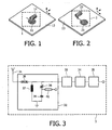
- the inductive-system 1 according to the invention shown in Fig. 1 comprises a printed coil 11 printed on a printed circuit board 13, and an air coil 12 mounted on the printed circuit board 13. Both coils 11,12 are coupled serially, with one end of the air coil 12 being coupled to a center end of the printed coil 11 and with the other end of the air coil 12 and the outer end of the printed coil 11 forming the ends of the inductive-system 1.
- the inductive-system 2 according to the invention shown in Fig. 2 comprises a printed coil 21 printed on a printed circuit board 23, and an air coil 22 mounted on the printed circuit board 23. Both coils 21,22 are coupled serially, with one end of the air coil 22 being coupled to an outer end of the printed coil 21 and with the other end of the air coil 22 and the inner end of the printed coil 21 forming the ends of the inductive-system 2.
- the tuner 3 according to the invention shown in Fig. 3 comprises an antenna input 31 to be coupled to an antenna or a cable or a satellite receiver etc.
- Antenna input 31 is coupled to an input of a filter 32, of which an output is coupled to an input of an amplifier 33, of which an output is coupled to an input of a bandpass filter 34, of which an output is coupled to an input of a mixer 35 etc.
- Filter 32 comprises a coil 36 coupled between the input and the output of the filter 32.
- Filter 32 further comprises a coil 37 coupled between the output of filter 32 and ground, and a serial circuit coupled in parallel to coil 37 and comprising a variable capacitor 38 and a capacitor 39.
- Each one of coils 36 and 37 may correspond with the inductive-system 1 or 2 as shown in Fig 1 or 2.
- Bandpass filter 34 may also comprise an inductive-system 1 or 2.
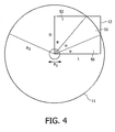
- the top view of a printed coil 11 and an air coil 12 as shown in Fig. 4 comprises the printed coil 11 having a radius (R 2 ) and the air coil 12 having a coil diameter (D) and a length (L).
- An overlapping area 50,51,52 comprises a first triangle 50 having a surface area equal to 0.5•L•R 2 •sin ( ⁇ ), a circle segment 51 having a surface area equal to 0.5• (R 2 ) 2 • ⁇ , and a second triangle 52 having a surface area equal to 0.5•D• R 2 •sin ( ⁇ ).
- the printed coil 11 comprises a number (n) of turns defined by at least one track width (w) and at least one turn spacing (s).
- the air coil 12 comprises a further number (T) of turns defined by at least one wire diameter (W) and at least one coil diameter (D).
- the number (n) of turns are further defined by a diameter of a center path (R 1 ) and a turning direction (d being clockwise or counterclockwise); with the further number (T) of turns being further defined by a turning orientation (O being left or right).
- the diameter of the center path (R 1 ) corresponds with a diameter of a most inner path, with the radius (R 2 ) corresponding with half the diameter of a most outer path.
- a total inductance of the inductive-system 1 is substantially equal to an inductance of the printed coil 11 plus an inductance of the air coil 12 plus a mutual inductance.
- the value of the mutual inductance is chosen by combining a right turn air coil or a left turn air coil with a clockwise printed coil or an counterclockwise printed coil and by selecting a length (L) of the air coil 12, with the mutual inductance increasing with the length (L) of the air coil 12 until a maximum overlapping area (50,51,52) between the printed coil 11 and the air coil 12 has been reached.
- the mutual inductance is relatively large negative for right turn air coils 12 combined with clockwise printed coils 11, and for left turn air coils 12 combined with counterclockwise printed coils 11.
- the mutual inductance is slightly negative for air coils having a relatively low number of turns (T) and increasingly positive for air coils having an increasing number of turns (T).
- the mutual inductance is relatively independent from the kind of layer (inner layer or outer layer) used for the printed coil 11.
- the inductive value of the printed coil 11 should be at most for example 1/3 of the inductive value of the inductive-system 1, to avoid that spreading in printed circuit board factors like etching accuracy and dielectric constant etc. get too much influence.
- the air coil 12 may have an inductance of about 200 nH and a Quality factor Q of about 100
- the printed coil 11 may have an inductance of about 150 nH and a Quality factor Q of about 65
- the inductive-system having an inductance of about 350 nH and a Quality factor Q of about 84.
- the printed coil 11,21 can be cylindrical, rectangular, hexagonal etc. and the air coil 12,22 can be cylindrical, rectangular, hexagonal etc. without departing from the scope of this invention. So, the word "turn” may be a kind of circular turn, a kind of rectangular turn, a kind of hexagonal turn etc.
- the invention is based upon an insight, inter alia, that large printed coils and large non-printed coils are to be avoided, and is based upon a basic idea, inter alia, that both kinds of coils can be combined efficiently by coupling them serially.
- the invention solves the problem, inter alia, of providing an inductive-system which, for relatively large inductive-values, is relatively small in size, and is advantageous, inter alia, in that the available room is used efficiently.
Landscapes
- Engineering & Computer Science (AREA)
- Power Engineering (AREA)
- Microelectronics & Electronic Packaging (AREA)
- Coils Or Transformers For Communication (AREA)
Abstract
Claims (9)
- Système inductif (1, 2) comprenant- une première partie sous la forme d'une bobine imprimée (11, 21) comprenant un certain nombre de spires défini par au moins une largeur de piste et au moins un espacement de spires ; et- une deuxième partie sous la forme d'une bobine non imprimée (12, 22) ; ladite bobine imprimée (11, 21) et ladite bobine non imprimée (12, 22) sont couplées en séries,dans lequel la bobine non imprimée (12, 22) comprend une bobine à air comprenant un autre nombre de spires défini par au moins un diamètre de fil et au moins un diamètre de bobine (D).
- Système inductif (12) tel que défini dans la revendication 2, dans lequel l'inductance totale I du système inductif (1, 2) est essentiellement égale à l'inductance de la bobine imprimée (11, 21) plus l'inductance de la bobine à air plus l'inductance mutuelle.
- Système inductif (1, 2) tel que défini dans la revendication 3, dans lequel une valeur de l'inductance mutuelle I a été choisie en combinant une bobine à air tournant à droite ou une bobine à air tournant à gauche avec une bobine imprimée tournant dans le sens des aiguilles d'une montre ou une bobine imprimée tournant dans le sens inverse des aiguilles d'une montre et en sélectionnant une longueur (L) de la bobine à air, dans laquelle l'inductance mutuelle augmente avec la longueur (L) de la bobine à air jusqu'à ce qu'une zone de superposition maximale (50, 51, 52) entre la bobine imprimée (11, 21) et la bobine à air ait été atteinte.
- Système inductif (1, 2) tel que défini dans la revendication 2, dans lequel le nombre de spires est en outre caractérisé par un diamètre d'un chemin central (Rat) et par un sens d'enroulement, le nombre supplémentaire de spires étant en outre caractérisé par un sens d'enroulement.
- Système inductif (1) tel que défini dans la revendication 1, dans lequel une extrémité de la bobine non imprimée (12) est couplée à une extrémité centrale de la bobine imprimée (11), l'autre extrémité de la bobine non imprimée (12) et une extrémité externe de la bobine imprimée (11) constituant les extrémités du système inductif (1).
- Système inductif (1, 2) tel que défini dans la revendication 1, dans lequel la bobine imprimée (11, 21) est imprimée sur une couche interne ou externe d'une carte à circuit imprimé (13, 23).
- Carte à circuit imprimé (13, 23) qui comprend un système inductif (1, 2) selon la revendication 1 et dans lequel la bobine imprimée (11, 21) est imprimée sur une couche interne ou externe de la carte à circuit imprimé (13, 23).
- Syntoniseur (3) qui comprend un filtre (32) avec un système inductif (1, 2) selon la revendication 1.
- Procédé de production d'un système inductif (1, 2) et comprenant les étapes de- production d'une première partie sous la forme d'une bobine imprimée (11, 21) comprenant un certain nombre de spires défini par une largeur d'au moins une piste et un espacement d'au moins un tour; production d'une deuxième partie sous la forme d'une bobine non imprimée (12, 22); et- couplage de la bobine imprimée (11, 21) et de la bobine non imprimée (12, 22) en séries,dans lequel la bobine non imprimée (12, 22) comprend une bobine à air comprenant un autre nombre de spires défini par au moins un diamètre de fil et au moins un diamètre de bobine (D).
Priority Applications (1)
| Application Number | Priority Date | Filing Date | Title |
|---|---|---|---|
| EP04737200A EP1647036B1 (fr) | 2003-07-11 | 2004-06-28 | Systeme inductif |
Applications Claiming Priority (3)
| Application Number | Priority Date | Filing Date | Title |
|---|---|---|---|
| EP03102113 | 2003-07-11 | ||
| PCT/IB2004/051021 WO2005006357A1 (fr) | 2003-07-11 | 2004-06-28 | Systeme inductif |
| EP04737200A EP1647036B1 (fr) | 2003-07-11 | 2004-06-28 | Systeme inductif |
Publications (2)
| Publication Number | Publication Date |
|---|---|
| EP1647036A1 EP1647036A1 (fr) | 2006-04-19 |
| EP1647036B1 true EP1647036B1 (fr) | 2007-11-21 |
Family
ID=34042940
Family Applications (1)
| Application Number | Title | Priority Date | Filing Date |
|---|---|---|---|
| EP04737200A Expired - Lifetime EP1647036B1 (fr) | 2003-07-11 | 2004-06-28 | Systeme inductif |
Country Status (7)
| Country | Link |
|---|---|
| US (1) | US20070018771A1 (fr) |
| EP (1) | EP1647036B1 (fr) |
| JP (1) | JP2007519218A (fr) |
| KR (1) | KR20060032196A (fr) |
| CN (1) | CN1823396B (fr) |
| DE (1) | DE602004010266T2 (fr) |
| WO (1) | WO2005006357A1 (fr) |
Families Citing this family (4)
| Publication number | Priority date | Publication date | Assignee | Title |
|---|---|---|---|---|
| CN1967267B (zh) * | 2006-10-29 | 2012-06-27 | 长沙同庆电气信息有限公司 | Pcb型空心线圈电流传感器 |
| GB2518476B (en) * | 2013-09-20 | 2015-11-04 | Silicon Lab Inc | Multi-chip modules having stacked television demodulators |
| US10396215B2 (en) * | 2015-03-10 | 2019-08-27 | United Silicon Carbide, Inc. | Trench vertical JFET with improved threshold voltage control |
| WO2017104454A1 (fr) * | 2015-12-14 | 2017-06-22 | 株式会社村田製作所 | Module à haute fréquence et module de transmission |
Family Cites Families (11)
| Publication number | Priority date | Publication date | Assignee | Title |
|---|---|---|---|---|
| US4035695A (en) * | 1974-08-05 | 1977-07-12 | Motorola, Inc. | Microelectronic variable inductor |
| JPH04801A (ja) * | 1990-04-17 | 1992-01-06 | Murata Mfg Co Ltd | バンドパスフィルタ |
| JP2713529B2 (ja) * | 1992-08-21 | 1998-02-16 | 三菱電機株式会社 | 信号受信用コイルおよびこれを使用した非接触icカード |
| JP3132297B2 (ja) * | 1994-07-28 | 2001-02-05 | 松下電器産業株式会社 | バランス型発振器とそれを用いた高周波装置 |
| JP3027112U (ja) * | 1996-01-23 | 1996-07-30 | 船井電機株式会社 | 巻線部品のプリント基板への取り付け構造 |
| US6163300A (en) * | 1997-08-07 | 2000-12-19 | Tokin Corporation | Multi-band antenna suitable for use in a mobile radio device |
| US6164241A (en) * | 1998-06-30 | 2000-12-26 | Lam Research Corporation | Multiple coil antenna for inductively-coupled plasma generation systems |
| JP2000278042A (ja) * | 1999-03-26 | 2000-10-06 | Sony Corp | 発振回路及びチューナ |
| JP3798195B2 (ja) * | 1999-08-12 | 2006-07-19 | ローム株式会社 | チップ型発光装置 |
| US7038294B2 (en) * | 2001-03-29 | 2006-05-02 | Taiwan Semiconductor Manufacturing Company, Ltd. | Planar spiral inductor structure with patterned microelectronic structure integral thereto |
| JP2003163403A (ja) * | 2001-11-29 | 2003-06-06 | Mitsubishi Electric Corp | 光素子モジュール |
-
2004
- 2004-06-28 EP EP04737200A patent/EP1647036B1/fr not_active Expired - Lifetime
- 2004-06-28 CN CN2004800199700A patent/CN1823396B/zh not_active Expired - Fee Related
- 2004-06-28 WO PCT/IB2004/051021 patent/WO2005006357A1/fr not_active Ceased
- 2004-06-28 JP JP2006518423A patent/JP2007519218A/ja not_active Withdrawn
- 2004-06-28 KR KR1020067000405A patent/KR20060032196A/ko not_active Withdrawn
- 2004-06-28 DE DE602004010266T patent/DE602004010266T2/de not_active Expired - Lifetime
- 2004-06-28 US US10/564,292 patent/US20070018771A1/en not_active Abandoned
Also Published As
| Publication number | Publication date |
|---|---|
| CN1823396B (zh) | 2010-05-12 |
| WO2005006357A1 (fr) | 2005-01-20 |
| KR20060032196A (ko) | 2006-04-14 |
| DE602004010266D1 (de) | 2008-01-03 |
| DE602004010266T2 (de) | 2008-11-06 |
| CN1823396A (zh) | 2006-08-23 |
| JP2007519218A (ja) | 2007-07-12 |
| EP1647036A1 (fr) | 2006-04-19 |
| US20070018771A1 (en) | 2007-01-25 |
Similar Documents
| Publication | Publication Date | Title |
|---|---|---|
| US6163300A (en) | Multi-band antenna suitable for use in a mobile radio device | |
| US7091814B2 (en) | On-chip differential multi-layer inductor | |
| US9385682B2 (en) | High frequency component and filter component | |
| US20020067235A1 (en) | High Q spiral inductor | |
| EP0795922A1 (fr) | Circuit d'adaptation et dispositif d'antenne | |
| US20070126544A1 (en) | Inductive component | |
| US10033103B2 (en) | Multilayer coil device, antenna module, and wireless communication module | |
| US6005467A (en) | Trimmable inductor | |
| US6975199B2 (en) | Embedded inductor and method of making | |
| US20120098728A1 (en) | Antenna module | |
| US11322284B2 (en) | High-frequency transformer and phase shifter | |
| AU744394B2 (en) | Compact antenna feed circuits | |
| GB2255692A (en) | Transponder tag having an adjustable inductance antenna | |
| JP2017212749A (ja) | 移相器、インピーダンス整合回路および通信端末装置 | |
| EP1647036B1 (fr) | Systeme inductif | |
| US5764197A (en) | Chip antenna | |
| US20210336648A1 (en) | Filter circuit module, filter circuit element, filter circuit, and communication apparatus | |
| JP2003197426A (ja) | インダクタンス素子を含む複合電子部品 | |
| JPH09307331A (ja) | 整合回路及びそれを用いたアンテナ装置 | |
| US7272884B2 (en) | Design and fabrication of inductors on a semiconductor substrate | |
| EP2433361B1 (fr) | Filtre de distribution de signaux tv équipé d'inducteurs plans | |
| WO2003092158A1 (fr) | Appareil a circuit multicouche offrant un couplage reduit | |
| JPH10256823A (ja) | ヘリカルアンテナ | |
| JP2005110144A (ja) | マッチング回路及びアンテナ装置 | |
| JPH023608Y2 (fr) |
Legal Events
| Date | Code | Title | Description |
|---|---|---|---|
| PUAI | Public reference made under article 153(3) epc to a published international application that has entered the european phase |
Free format text: ORIGINAL CODE: 0009012 |
|
| 17P | Request for examination filed |
Effective date: 20060213 |
|
| AK | Designated contracting states |
Kind code of ref document: A1 Designated state(s): AT BE BG CH CY CZ DE DK EE ES FI FR GB GR HU IE IT LI LU MC NL PL PT RO SE SI SK TR |
|
| DAX | Request for extension of the european patent (deleted) | ||
| GRAP | Despatch of communication of intention to grant a patent |
Free format text: ORIGINAL CODE: EPIDOSNIGR1 |
|
| RAP1 | Party data changed (applicant data changed or rights of an application transferred) |
Owner name: NXP B.V. |
|
| GRAS | Grant fee paid |
Free format text: ORIGINAL CODE: EPIDOSNIGR3 |
|
| GRAA | (expected) grant |
Free format text: ORIGINAL CODE: 0009210 |
|
| AK | Designated contracting states |
Kind code of ref document: B1 Designated state(s): AT BE BG CH CY CZ DE DK EE ES FI FR GB GR HU IE IT LI LU MC NL PL PT RO SE SI SK TR |
|
| REG | Reference to a national code |
Ref country code: GB Ref legal event code: FG4D |
|
| REG | Reference to a national code |
Ref country code: IE Ref legal event code: FG4D |
|
| REG | Reference to a national code |
Ref country code: CH Ref legal event code: EP |
|
| REF | Corresponds to: |
Ref document number: 602004010266 Country of ref document: DE Date of ref document: 20080103 Kind code of ref document: P |
|
| ET | Fr: translation filed | ||
| PG25 | Lapsed in a contracting state [announced via postgrant information from national office to epo] |
Ref country code: NL Free format text: LAPSE BECAUSE OF FAILURE TO SUBMIT A TRANSLATION OF THE DESCRIPTION OR TO PAY THE FEE WITHIN THE PRESCRIBED TIME-LIMIT Effective date: 20071121 Ref country code: SE Free format text: LAPSE BECAUSE OF FAILURE TO SUBMIT A TRANSLATION OF THE DESCRIPTION OR TO PAY THE FEE WITHIN THE PRESCRIBED TIME-LIMIT Effective date: 20080221 Ref country code: CH Free format text: LAPSE BECAUSE OF FAILURE TO SUBMIT A TRANSLATION OF THE DESCRIPTION OR TO PAY THE FEE WITHIN THE PRESCRIBED TIME-LIMIT Effective date: 20071121 Ref country code: LI Free format text: LAPSE BECAUSE OF FAILURE TO SUBMIT A TRANSLATION OF THE DESCRIPTION OR TO PAY THE FEE WITHIN THE PRESCRIBED TIME-LIMIT Effective date: 20071121 Ref country code: ES Free format text: LAPSE BECAUSE OF FAILURE TO SUBMIT A TRANSLATION OF THE DESCRIPTION OR TO PAY THE FEE WITHIN THE PRESCRIBED TIME-LIMIT Effective date: 20080304 |
|
| NLV1 | Nl: lapsed or annulled due to failure to fulfill the requirements of art. 29p and 29m of the patents act | ||
| PG25 | Lapsed in a contracting state [announced via postgrant information from national office to epo] |
Ref country code: SI Free format text: LAPSE BECAUSE OF FAILURE TO SUBMIT A TRANSLATION OF THE DESCRIPTION OR TO PAY THE FEE WITHIN THE PRESCRIBED TIME-LIMIT Effective date: 20071121 Ref country code: PL Free format text: LAPSE BECAUSE OF FAILURE TO SUBMIT A TRANSLATION OF THE DESCRIPTION OR TO PAY THE FEE WITHIN THE PRESCRIBED TIME-LIMIT Effective date: 20071121 Ref country code: BG Free format text: LAPSE BECAUSE OF FAILURE TO SUBMIT A TRANSLATION OF THE DESCRIPTION OR TO PAY THE FEE WITHIN THE PRESCRIBED TIME-LIMIT Effective date: 20080221 Ref country code: FI Free format text: LAPSE BECAUSE OF FAILURE TO SUBMIT A TRANSLATION OF THE DESCRIPTION OR TO PAY THE FEE WITHIN THE PRESCRIBED TIME-LIMIT Effective date: 20071121 |
|
| REG | Reference to a national code |
Ref country code: CH Ref legal event code: PL |
|
| PG25 | Lapsed in a contracting state [announced via postgrant information from national office to epo] |
Ref country code: AT Free format text: LAPSE BECAUSE OF FAILURE TO SUBMIT A TRANSLATION OF THE DESCRIPTION OR TO PAY THE FEE WITHIN THE PRESCRIBED TIME-LIMIT Effective date: 20071121 |
|
| PG25 | Lapsed in a contracting state [announced via postgrant information from national office to epo] |
Ref country code: CZ Free format text: LAPSE BECAUSE OF FAILURE TO SUBMIT A TRANSLATION OF THE DESCRIPTION OR TO PAY THE FEE WITHIN THE PRESCRIBED TIME-LIMIT Effective date: 20071121 Ref country code: DK Free format text: LAPSE BECAUSE OF FAILURE TO SUBMIT A TRANSLATION OF THE DESCRIPTION OR TO PAY THE FEE WITHIN THE PRESCRIBED TIME-LIMIT Effective date: 20071121 |
|
| PG25 | Lapsed in a contracting state [announced via postgrant information from national office to epo] |
Ref country code: SK Free format text: LAPSE BECAUSE OF FAILURE TO SUBMIT A TRANSLATION OF THE DESCRIPTION OR TO PAY THE FEE WITHIN THE PRESCRIBED TIME-LIMIT Effective date: 20071121 Ref country code: BE Free format text: LAPSE BECAUSE OF FAILURE TO SUBMIT A TRANSLATION OF THE DESCRIPTION OR TO PAY THE FEE WITHIN THE PRESCRIBED TIME-LIMIT Effective date: 20071121 Ref country code: RO Free format text: LAPSE BECAUSE OF FAILURE TO SUBMIT A TRANSLATION OF THE DESCRIPTION OR TO PAY THE FEE WITHIN THE PRESCRIBED TIME-LIMIT Effective date: 20071121 |
|
| PLBE | No opposition filed within time limit |
Free format text: ORIGINAL CODE: 0009261 |
|
| STAA | Information on the status of an ep patent application or granted ep patent |
Free format text: STATUS: NO OPPOSITION FILED WITHIN TIME LIMIT |
|
| PG25 | Lapsed in a contracting state [announced via postgrant information from national office to epo] |
Ref country code: PT Free format text: LAPSE BECAUSE OF FAILURE TO SUBMIT A TRANSLATION OF THE DESCRIPTION OR TO PAY THE FEE WITHIN THE PRESCRIBED TIME-LIMIT Effective date: 20080421 |
|
| 26N | No opposition filed |
Effective date: 20080822 |
|
| PG25 | Lapsed in a contracting state [announced via postgrant information from national office to epo] |
Ref country code: GR Free format text: LAPSE BECAUSE OF FAILURE TO SUBMIT A TRANSLATION OF THE DESCRIPTION OR TO PAY THE FEE WITHIN THE PRESCRIBED TIME-LIMIT Effective date: 20080222 Ref country code: MC Free format text: LAPSE BECAUSE OF NON-PAYMENT OF DUE FEES Effective date: 20080630 |
|
| PG25 | Lapsed in a contracting state [announced via postgrant information from national office to epo] |
Ref country code: EE Free format text: LAPSE BECAUSE OF FAILURE TO SUBMIT A TRANSLATION OF THE DESCRIPTION OR TO PAY THE FEE WITHIN THE PRESCRIBED TIME-LIMIT Effective date: 20071121 Ref country code: IE Free format text: LAPSE BECAUSE OF NON-PAYMENT OF DUE FEES Effective date: 20080630 |
|
| PG25 | Lapsed in a contracting state [announced via postgrant information from national office to epo] |
Ref country code: CY Free format text: LAPSE BECAUSE OF FAILURE TO SUBMIT A TRANSLATION OF THE DESCRIPTION OR TO PAY THE FEE WITHIN THE PRESCRIBED TIME-LIMIT Effective date: 20071121 |
|
| PG25 | Lapsed in a contracting state [announced via postgrant information from national office to epo] |
Ref country code: LU Free format text: LAPSE BECAUSE OF NON-PAYMENT OF DUE FEES Effective date: 20080628 Ref country code: HU Free format text: LAPSE BECAUSE OF FAILURE TO SUBMIT A TRANSLATION OF THE DESCRIPTION OR TO PAY THE FEE WITHIN THE PRESCRIBED TIME-LIMIT Effective date: 20080522 |
|
| PGFP | Annual fee paid to national office [announced via postgrant information from national office to epo] |
Ref country code: FR Payment date: 20100709 Year of fee payment: 7 |
|
| PG25 | Lapsed in a contracting state [announced via postgrant information from national office to epo] |
Ref country code: TR Free format text: LAPSE BECAUSE OF FAILURE TO SUBMIT A TRANSLATION OF THE DESCRIPTION OR TO PAY THE FEE WITHIN THE PRESCRIBED TIME-LIMIT Effective date: 20071121 |
|
| PGFP | Annual fee paid to national office [announced via postgrant information from national office to epo] |
Ref country code: DE Payment date: 20100625 Year of fee payment: 7 Ref country code: GB Payment date: 20100623 Year of fee payment: 7 |
|
| PG25 | Lapsed in a contracting state [announced via postgrant information from national office to epo] |
Ref country code: IT Free format text: LAPSE BECAUSE OF NON-PAYMENT OF DUE FEES Effective date: 20080630 |
|
| GBPC | Gb: european patent ceased through non-payment of renewal fee |
Effective date: 20110628 |
|
| REG | Reference to a national code |
Ref country code: FR Ref legal event code: ST Effective date: 20120229 |
|
| REG | Reference to a national code |
Ref country code: DE Ref legal event code: R119 Ref document number: 602004010266 Country of ref document: DE Effective date: 20120103 |
|
| PG25 | Lapsed in a contracting state [announced via postgrant information from national office to epo] |
Ref country code: DE Free format text: LAPSE BECAUSE OF NON-PAYMENT OF DUE FEES Effective date: 20120103 Ref country code: FR Free format text: LAPSE BECAUSE OF NON-PAYMENT OF DUE FEES Effective date: 20110630 |
|
| PG25 | Lapsed in a contracting state [announced via postgrant information from national office to epo] |
Ref country code: GB Free format text: LAPSE BECAUSE OF NON-PAYMENT OF DUE FEES Effective date: 20110628 |