EP1652973A1 - Monocristal et substrat de carbure de silicium et procédé pour la fabrication d'un monocristal de carbure de silicium - Google Patents
Monocristal et substrat de carbure de silicium et procédé pour la fabrication d'un monocristal de carbure de silicium Download PDFInfo
- Publication number
- EP1652973A1 EP1652973A1 EP05023532A EP05023532A EP1652973A1 EP 1652973 A1 EP1652973 A1 EP 1652973A1 EP 05023532 A EP05023532 A EP 05023532A EP 05023532 A EP05023532 A EP 05023532A EP 1652973 A1 EP1652973 A1 EP 1652973A1
- Authority
- EP
- European Patent Office
- Prior art keywords
- content
- single crystal
- dopant
- atoms
- silicon carbide
- Prior art date
- Legal status (The legal status is an assumption and is not a legal conclusion. Google has not performed a legal analysis and makes no representation as to the accuracy of the status listed.)
- Granted
Links
Images
Classifications
-
- C—CHEMISTRY; METALLURGY
- C30—CRYSTAL GROWTH
- C30B—SINGLE-CRYSTAL GROWTH; UNIDIRECTIONAL SOLIDIFICATION OF EUTECTIC MATERIAL OR UNIDIRECTIONAL DEMIXING OF EUTECTOID MATERIAL; REFINING BY ZONE-MELTING OF MATERIAL; PRODUCTION OF A HOMOGENEOUS POLYCRYSTALLINE MATERIAL WITH DEFINED STRUCTURE; SINGLE CRYSTALS OR HOMOGENEOUS POLYCRYSTALLINE MATERIAL WITH DEFINED STRUCTURE; AFTER-TREATMENT OF SINGLE CRYSTALS OR A HOMOGENEOUS POLYCRYSTALLINE MATERIAL WITH DEFINED STRUCTURE; APPARATUS THEREFOR
- C30B29/00—Single crystals or homogeneous polycrystalline material with defined structure characterised by the material or by their shape
- C30B29/10—Inorganic compounds or compositions
- C30B29/36—Carbides
-
- C—CHEMISTRY; METALLURGY
- C30—CRYSTAL GROWTH
- C30B—SINGLE-CRYSTAL GROWTH; UNIDIRECTIONAL SOLIDIFICATION OF EUTECTIC MATERIAL OR UNIDIRECTIONAL DEMIXING OF EUTECTOID MATERIAL; REFINING BY ZONE-MELTING OF MATERIAL; PRODUCTION OF A HOMOGENEOUS POLYCRYSTALLINE MATERIAL WITH DEFINED STRUCTURE; SINGLE CRYSTALS OR HOMOGENEOUS POLYCRYSTALLINE MATERIAL WITH DEFINED STRUCTURE; AFTER-TREATMENT OF SINGLE CRYSTALS OR A HOMOGENEOUS POLYCRYSTALLINE MATERIAL WITH DEFINED STRUCTURE; APPARATUS THEREFOR
- C30B23/00—Single-crystal growth by condensing evaporated or sublimed materials
-
- Y—GENERAL TAGGING OF NEW TECHNOLOGICAL DEVELOPMENTS; GENERAL TAGGING OF CROSS-SECTIONAL TECHNOLOGIES SPANNING OVER SEVERAL SECTIONS OF THE IPC; TECHNICAL SUBJECTS COVERED BY FORMER USPC CROSS-REFERENCE ART COLLECTIONS [XRACs] AND DIGESTS
- Y10—TECHNICAL SUBJECTS COVERED BY FORMER USPC
- Y10S—TECHNICAL SUBJECTS COVERED BY FORMER USPC CROSS-REFERENCE ART COLLECTIONS [XRACs] AND DIGESTS
- Y10S438/00—Semiconductor device manufacturing: process
- Y10S438/931—Silicon carbide semiconductor
Definitions
- the present invention relates to silicon carbide (SiC) single crystal, a SiC substrate and a manufacturing method for SiC single crystal, and in particular, to p type SiC single crystal having high resistivity, a SiC substrate and a manufacturing method for SiC single crystal.
- SiC silicon carbide
- SiC has a band gap that is approximately 3 times greater than that of silicon (Si), a dielectric breakdown voltage that is approximately 10 times higher than that of Si, an electron saturation speed that is approximately twice greater than that of Si, and thermal conductivity that is approximately 3 times greater than that of Si, as well as properties that Si does not have.
- SiC is a thermally and chemically stable semiconductor material, and on the basis of these properties, and, in recent years, has come to be expected to be applied to power devices that exceed the physical limit of Si devices, or to environment resistant devices that operate at a high temperatures.
- GaN gallium nitride
- a substrate having a low resistivity is required as a substrate for a semiconductor laser
- a substrate having high resistivity is required as a substrate for a high frequency device, so that the parasitic capacitance can be reduced, element isolation can be gained and the like.
- a SiC substrate having low resistivity can be gained relatively easily, for example, by mixing a nitrogen gas with an argon gas, which is an atmospheric gas, in an improved Rayleigh method.
- a SiC substrate having high resistivity can be manufactured by cutting SiC single crystal containing vanadium and having high resistivity, as described in, for example, U.S. Patent No. 5,611,955, PCT National Publication No. 2003-500321, and Japanese Patent Laying-Open No. 2003-104798.
- Such SiC single crystal containing vanadium and having high resistivity can be manufactured by adding highly pure metal vanadium to a highly pure SiC crystal powder, and by sublimating the metal vanadium together with SiC, so that vanadium is contained in the SiC single crystal.
- Japanese Patent Laying-Open No. 2003-104798 discloses a method for manufacturing SiC crystal that contains vanadium in advance, and then converting it into powder form, and re-growing SiC single crystal that contains vanadium from this raw material in accordance with an improved Rayleigh method.
- this method it is necessary to manufacture SiC crystal that contains vanadium in advance, and therefore, a problem arises, where SiC single crystal having high resistivity cannot be efficiently manufactured.
- SiC substrate having high resistivity can be fabricated by increasing the purity of SiC single crystal instead of adding vanadium as described above.
- SiC single crystal that has been fabricated in accordance with a high temperature CVD method which is a specialized chemical vapor deposition (CVD) method, for example, tends to have high purity.
- CVD chemical vapor deposition
- An object of the present invention is to provide SiC single crystal and a SiC substrate having high resistivity.
- an object of the present invention is to provide a manufacturing method for SiC single crystal according to which SiC single crystal stably having high resistivity can be manufactured.
- the present invention provides SiC single crystal that includes a first dopant functioning as an acceptor, and a second dopant functioning as a donor, where the content of the first dopant is no less than 5 ⁇ 10 15 atoms/cm 3 , the content of the second dopant is no less than 5 ⁇ 10 15 atoms/cm 3 , and the content of the first dopant is greater than the content of the second dopant.
- the content of the first dopant is no less than 1 x 10 16 atoms/cm 3 and no greater than 1 x 10 17 atoms/cm 3 .
- the content of the second dopant is no less than 1 ⁇ 10 16 atoms/cm 3 .
- the difference between the content of the first dopant and the content of the second dopant is no greater than 5 x 10 16 atoms/cm 3 .
- the first dopant prefferably be boron and for the second dopant to be nitrogen.
- the resistivity at 25 °C is no less than 1 ⁇ 10 4 ⁇ cm.
- the resistivity at 25 °C is no less than 1 x 10 7 ⁇ cm.
- the present invention provides a SiC substrate made of SiC single crystal, as described above.
- the present invention provided a manufacturing method for silicon carbide single crystal that includes the steps of: fabricating a raw material by mixing a metal boride with a material that includes carbon and silicon; vaporizing the raw material; generating a mixed gas that includes carbon, silicon, boron and nitrogen; and growing silicon carbide single crystal that includes boron and nitrogen on a surface of a seed crystal substrate by re-crystallizing the mixed gas on the surface of the seed substrate.
- the metal boride prefferably be at least one type of substance selected from the group of titanium boride, zirconium boride, hafnium boride, tantalum boride and niobium boride.
- the present invention can provide SiC single crystal and a SiC substrate having high resistivity.
- the present invention can provide a manufacturing method for SiC single crystal according to which SiC single crystal having high resistivity can be stably manufactured.
- the present invention provides SiC single crystal that includes a first dopant functioning as an acceptor, and a second dopant functioning as a donor, wherein the content of the first dopant is no less than 5 x 10 15 atoms/cm 3 , the content of the second dopant is no less than 5 x 10 15 atoms/cm 3 , and the content of the first dopant is greater than the content of the second dopant.
- the content of the first dopant in the SiC single crystal is no less than 1 x 10 16 atoms/cm 3 and no greater than 1 x 10 17 atoms/cm 3 .
- the content of the first dopant in the SiC single crystal is too small, causing scattering of electrons due to the first dopant to be insufficient, and the SiC single crystal tends not to have high resistivity, and in the case where the content of the first dopant is greater than 1 ⁇ 10 17 atoms/cm 3 , the crystallinity of the SiC single crystal tends to deteriorate.
- the content of the second dopant in the SiC single crystal is no less than 1 ⁇ 10 16 atoms/cm 3 .
- the content of the second dopant in the SiC single crystal is too small, causing scattering of electrons due to the second dopant to be insufficient, and the SiC single crystal tends not to have high resistivity.
- the difference between the content of the first dopant and the content of the second dopant is no greater than 5 x 10 16 atoms/cm 3 .
- the difference between the content of the first dopant and the content of the second dopant is greater than 5 x 10 16 atoms/cm 3 , reduction in the number of carriers due to the compensation between the first dopant and the second dopant is not sufficient, and the resistivity of the SiC single crystal tends to become low.
- the first dopant functioning as an acceptor is a dopant that functions as an electron receptor in SiC single crystal.
- Boron, aluminum and gallium, for example, can be cited as the first dopant, and in particular, boron is preferable. This is because boron has deep level and SiC single crystal that includes boron tends to have high resistivity.
- the second dopant functioning as a donor is a dopant that functions as an electron donor in SiC single crystal.
- Nitrogen and phosphorous for example, can be cited as the second dopant, and in particular, nitrogen is preferable. This is because in the case where nitrogen is used as the second dopant, the manufacture of SiC single crystal tends to become easy.
- the resistivity of the SiC single crystal at 25°C in the present invention is no less than 1 ⁇ 10 4 ⁇ cm, and it is more preferable for it to be no less than 1 ⁇ 10 7 ⁇ cm.
- the resistivity of the SiC single crystal at 25 °C in the present invention is no less than 1 ⁇ 10 4 ⁇ cm
- the SiC single crystal of the present invention is appropriate for use as a substrate for a semiconductor device that requires an insulating substrate.
- the resistivity at 25°C is no less than 1 ⁇ 10 7 ⁇ cm
- the SiC single crystal of the present invention is more appropriate for use as a substrate for a semiconductor device that requires an insulating substrate.
- a manufacturing method for such SiC single crystal of the present invention there is a manufacturing method that includes the steps of: fabricating a raw material by mixing a metal boride with a material that includes carbon and silicon; vaporizing the raw material; generating a mixed gas that includes carbon, silicon, boron and nitrogen; and growing SiC single crystal that contains boron and nitrogen on a surface of a seed crystal substrate by re-crystallizing the mixed gas on the surface of the seed crystal substrate.
- a metal boride includes titanium boride, zirconium boride, hafnium boride, tantalum boride, niobium boride, aluminum boride, ytterbium boride, uranium boride, gadolinium boride, calcium boride, chromium boride, silicon boride, cobalt boride, strontium boride, tungsten boride, iron boride, copper boride, thorium boride, nickel boride, barium boride, magnesium boride, manganese boride, molybdenum boride, vanadium boride and cerium boride.
- the metal boride it is preferable to use at least one type of substance selected from the group of titanium boride, zirconium boride, hafnium boride, tantalum boride and niobium boride as the metal boride.
- these metal borides have a vapor pressure that is lower than that of single boron, and therefore, a large amount of boron is not taken in by SiC single crystal at the initial stage of growth of the SiC single crystal, unlike in the case where metal boron is used, and boron can be uniformly taken in by the SiC single crystal.
- the dimensions of atoms of boron in these metal borides are not so different from those of carbon, and therefore, boron tends to be taken into carbon sites in the SiC single crystal, while metal in the metal borides has atoms that are greater than those of silicon and carbon, and therefore, metal in the metal borides tends not to be taken into silicon sites and carbon sites in the SiC single crystal.
- a raw material where a metal boride is mixed with a material that includes carbon and silicon is heated to a temperature of, for example, no lower than 2000 °C and no higher than 2800 °C, so as to be vaporized into a vapor gas with which a nitrogen gas is then mixed, and thus, a mixed gas that includes carbon, silicon, boron and nitrogen is generated.
- the content of boron in the mixed gas is made to be no less than 2 x 10 -3 mol% of the content of silicon in the mixed gas, and thereby, the content of boron in the SiC single crystal can be made to be no less than 5 x 10 15 atoms/cm 3 .
- the content of nitrogen in the mixed gas is made to be no less than 2 x 10 -3 mol% of the content of silicon in the mixed gas, and thereby, the content of nitrogen in the SiC single crystal can be made to be no less than 5 x 10 15 atoms/cm 3 .
- the content of boron in the mixed gas is made to be no less than 4 x 10 -3 mol% and no greater than 4 x 10 -1 mol% of silicon in the mixed gas by adjusting the mixed amount of the metal boride
- the content of boron in the SiC single crystal can be made to be no less than 1 x 10 16 atoms/cm 3 and no greater than 1 ⁇ 10 17 atoms/cm 3 .
- the content of nitrogen in the mixed gas is made to be no less than 4 x 10 -3 mol% of silicon in the mixed gas by adjusting the mixed amount of the nitrogen gas
- the content of nitrogen in the SiC single crystal can be made to be no less than 1 x 10 16 atoms/cm 3 .
- the difference in content between boron and nitrogen in the SiC single crystal can be made to be no greater than 5 ⁇ 10 16 atoms/cm 3 , by appropriately adjusting the mixed amount of the metal boride and the mixed amount of the nitrogen gas.
- this mixed gas is re-crystallized on a surface of a seed crystal substrate, and thereby, SiC single crystal is grown on the surface of the seed crystal substrate, and the SiC single crystal of the present invention can be manufactured,
- the SiC single crystal that has been manufactured in this manner is cut, and thereby, a SiC substrate of the present invention can be manufactured.
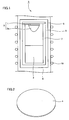
- Fig. 1 is a schematic cross sectional diagram showing a SiC single crystal growing apparatus that is used in the present invention.
- This growing apparatus 5 includes a crucible 7 made of graphite that is installed inside a crystal tube 6, a lid 8 for closing the opening on the upper end of the crucible 7, a felt 9 made of graphite for heat shielding that is installed around crucible 7 and lid 8, and a work coil 10 that is installed so as to wind around the outer periphery of crystal tube 6.
- a seed crystal substrate 1 made of SiC is attached to the center of the lower surface of lid 8, and the inside of crucible 7 is filled in with a raw material 2.
- Raw material 2 was manufactured by mixing 2 x 10 -2 mol% of titanium boride (TiB 2 ) relative to the amount of substance of silicon in raw material 2 with a SiC crystal powder.
- TiB 2 titanium boride
- the pressure inside crucible 7 was once reduced to 10 -5 Pa, and after that, an argon (Ar) gas was introduced, so that the inside of crucible 7 was filled with an Ar gas atmosphere, under a pressure of 1 x 10 5 Pa.
- a high frequency current was made to flow through work coil 10, so as to heat raw material 2 to 2200 °C, and the pressure on the inside of crucible 7 was reduced to 1.3 x 10 3 Pa, so as to vaporize raw material 2, and this vaporous gas was mixed with a nitrogen gas so as to gain a mixed gas.
- the content of nitrogen in the mixed gas was 2 x 10 -2 mol% of the content of silicon in the mixed gas.
- heating was carried out by work coil 10, with a temperature gradient such that the temperature gradually decreased from raw material 2 to SiC seed crystal substrate 1. After that, the mixed gas was re-crystallized on the surface of SiC seed crystal substrate 1, and thereby, SiC single crystal 2a grew, and a SiC single crystal ingot 3 was gained.
- This SiC single crystal ingot 3 was cut into slices having a thickness of 400 ⁇ m, and a SiC substrate 4 in disc form having a diameter of 2 inches, as shown in Fig. 2, was manufactured. Then, the content of boron and nitrogen in this SiC substrate 4 was measured by means of SIMS (secondary ion mass spectrometry), and thus, the difference in content between boron and nitrogen was calculated. In addition, the resistivity of this SiC substrate was measured. The results are shown in Table 1. As shown in Table 1, the content of boron in this SiC substrate was 1 ⁇ 10 17 atoms/cm 3 , and the content of nitrogen was 5 ⁇ 10 16 atoms/cm 3 . In addition, the difference in content between boron and nitrogen was 5 x 10 16 atoms/cm 3 . Furthermore, the resistivity of the SiC substrate was 1 x 10 5 ⁇ cm.
- a SiC substrate was manufactured in the same manner as in the example 1, except that the content of nitrogen in the mixed gas was made to be 3.5 x 10 -2 mol% of the content of silicon in the mixed gas. Then, the content of boron and nitrogen in this SiC substrate was measured in the same manner as in the example 1, and thus, the difference in content between boron and nitrogen was calculated. In addition, the resistivity of this SiC substrate was measured. The results are shown in Table 1. As shown in Table 1, the content of boron in this SiC substrate was 1 ⁇ 10 17 atoms/cm 3 , and the content of nitrogen was 8 ⁇ 10 16 atoms/cm 3 . In addition, the difference in content between boron and nitrogen was 2 ⁇ 10 16 atoms/cm 3 . Furthermore, the resistivity of this SiC substrate was 1 ⁇ 10 6 ⁇ cm.
- a SiC substrate was manufactured in the same manner as in the example 1, except that 0.4 x 10 -2 mol% of TiB 2 relative to the amount of substance of silicon in raw material 2, shown in Fig. 1, was mixed in, and the content of nitrogen in the mixed gas was made to be 0.4 x 10 -2 mol% of the content of silicon in the mixed gas. Then, the content of boron and nitrogen in this SiC substrate was measured in the same manner as in the example 1, and thus, the difference in content between boron and nitrogen was calculated. In addition, the resistivity of this SiC substrate was measured. The results are shown in Table 1.
- the content of boron in this SiC substrate was 2 x 10 16 atoms/cm 3
- the content of nitrogen was 1 x 10 16 atoms/cm 3
- the difference in content between boron and nitrogen was 1 x 10 16 atoms/cm 3
- the resistivity of this SiC substrate was 1 x 10 7 ⁇ cm.
- a SiC substrate was manufactured in the same manner as in the example 1, except that 2 x 10 -3 mol% of TiB 2 relative to the amount of substance of silicon in raw material 2, shown in Fig. 1, was mixed in, and the content of nitrogen in the mixed gas was made to be 2 x 10 -3 mol% of the content of silicon in the mixed gas. Then, the content of boron and nitrogen in this SiC substrate was measured in the same manner as in the example 1, and thus, the difference in content between boron and nitrogen was calculated. In addition, the resistivity of this SiC substrate was measured. The results are shown in Table 1.
- the content of boron in this SiC substrate was 1 ⁇ 10 16 atoms/cm 3
- the content of nitrogen was 5 ⁇ 10 15 atoms/cm 3
- the difference in content between boron and nitrogen was 5 ⁇ 10 15 atoms/cm 3
- the resistivity of this SiC substrate was 1 ⁇ 10 7 ⁇ cm.
- a SiC substrate was manufactured in the same manner as in the example 1, except that 1.9 x 10 -3 mol% of TiB 2 relative to the amount of substance of silicon in raw material 2, shown in Fig. 1, was mixed in, and the content of nitrogen in the mixed gas was made to be 2 x 10 -3 mol% of the content of silicon in the mixed gas. Then, the content of boron and nitrogen in this SiC substrate was measured in the same manner as in the example 1, and thus, the difference in content between boron and nitrogen was calculated. In addition, the resistivity of this SiC substrate was measured. The results are shown in Table 1.
- the content of boron in this SiC substrate was 9.5 x 10 15 atoms/cm 3
- the content of nitrogen was 5 x 10 15 atoms/cm 3
- the difference in content between boron and nitrogen was 4.5 x 10 15 atoms/cm 3
- the resistivity of this SiC substrate was 5 ⁇ 10 9 ⁇ cm.
- a SiC substrate was manufactured in the same manner as in the first example 1, except that 1.02 x 10 -3 mol% of TiB 2 relative to the amount of substance of silicon in raw material 2, shown in Fig. 1, was mixed in, and the content of nitrogen in the mixed gas was made to be 2 ⁇ 10 -3 mol% of the content of silicon in the mixed gas. Then, the content of boron and nitrogen in this SiC substrate was measured in the same manner as in the example 1, and thus, the difference in content between boron and nitrogen was calculated. In addition, the resistivity of this SiC substrate was measured. The results are shown in Table 1.
- the content of boron in this SiC substrate was 5.1 x 10 15 atoms/cm 3
- the content of nitrogen was 5.0 x 10 15 atoms/cm 3
- the difference in content between boron and nitrogen was 1.0 x 10 14 atoms/cm 3
- the resistivity of this SiC substrate was 1.0 x 10 11 ⁇ cm.
- a SiC substrate was manufactured in the same manner as in the example 1, except that 2 ⁇ 10 -2 mol% of TiB 2 relative to the amount of substance of silicon in raw material 2, shown in Fig. 1, was mixed in, and the content of nitrogen in the mixed gas was made to be 1.6 x 10 -2 mol% of the content of silicon in the mixed gas. Then, the content of boron and nitrogen in this SiC substrate was measured in the same manner as in the example 1, and thus, the difference in content between boron and nitrogen was calculated. In addition, the resistivity of this SiC substrate was measured. The results are shown in Table 1.
- the content of boron in this SiC substrate was 1 ⁇ 10 17 atoms/cm 3
- the content of nitrogen was 4 ⁇ 10 16 atoms/cm 3
- the difference in content between boron and nitrogen was 6 x 10 16 atoms/cm 3
- the resistivity of this SiC substrate was 1.1 ⁇ 10 2 ⁇ cm.
- a SiC substrate was manufactured in the same manner as in the example 1, except that 0.98 x 10 -3 mol% of TiB 2 relative to the amount of substance of silicon in raw material 2, shown in Fig. 1, was mixed in, and the content of nitrogen in the mixed gas was made to be 1 x 10 -3 mol% of the content of silicon in the mixed gas. Then, the content of boron and nitrogen in this SiC substrate was measured in the same manner as in the example 1, and thus, the difference in content between boron and nitrogen was calculated. In addition, the resistivity of this SiC substrate was measured. The results are shown in Table 1.
- the content of boron in this SiC substrate was 4.9 x 10 15 atoms/cm 3
- the content of nitrogen was 2.5 x 10 15 atoms/cm 3
- the difference in content between boron and nitrogen was 2.4 x 10 15 atoms/cm 3
- the resistivity of this SiC substrate was 1 ⁇ 10 4 ⁇ cm.
- a SiC substrate was manufactured in the same manner as in the example 1, except that 2 x 10 -3 mol% of TiB 2 relative to the amount of substance of silicon in raw material 2, shown in Fig. 1, was mixed in, and the content of nitrogen in the mixed gas was made to be 1 x 10 -2 mol% of the content of silicon in the mixed gas. Then, the content of boron and nitrogen in this SiC substrate was measured in the same manner as in the example 1, and thus, the difference in content between boron and nitrogen was calculated. In addition, the resistivity of this SiC substrate was measured. The results are shown in Table 1.
- the content of boron in this SiC substrate was 1 ⁇ 10 16 atoms/cm 3
- the content of nitrogen was 2.5 ⁇ 10 16 atoms/cm 3
- the difference in content between boron and nitrogen was -1.5 ⁇ 10 16 atoms/cm 3
- the resistivity of this SiC substrate was 1 ⁇ 10 -1 ⁇ cm.
- TiB 2 was used as a metal boride in the above-described example, the same effects as those in the above-described examples can, of course, be gained even in the case where a metal boride other than TiB 2 is used.
- the present invention is appropriate for application to high frequency devices, in particular, switching elements having a high operation frequency in the field of semiconductor devices.
Landscapes
- Chemical & Material Sciences (AREA)
- Engineering & Computer Science (AREA)
- Crystallography & Structural Chemistry (AREA)
- Materials Engineering (AREA)
- Metallurgy (AREA)
- Organic Chemistry (AREA)
- Inorganic Chemistry (AREA)
- Crystals, And After-Treatments Of Crystals (AREA)
Applications Claiming Priority (1)
| Application Number | Priority Date | Filing Date | Title |
|---|---|---|---|
| JP2004316458A JP4470690B2 (ja) | 2004-10-29 | 2004-10-29 | 炭化珪素単結晶、炭化珪素基板および炭化珪素単結晶の製造方法 |
Publications (2)
| Publication Number | Publication Date |
|---|---|
| EP1652973A1 true EP1652973A1 (fr) | 2006-05-03 |
| EP1652973B1 EP1652973B1 (fr) | 2011-08-10 |
Family
ID=35482186
Family Applications (1)
| Application Number | Title | Priority Date | Filing Date |
|---|---|---|---|
| EP05023532A Expired - Lifetime EP1652973B1 (fr) | 2004-10-29 | 2005-10-27 | Monocristal et substrat de carbure de silicium et procédé pour la fabrication d'un monocristal de carbure de silicium |
Country Status (6)
| Country | Link |
|---|---|
| US (1) | US8013343B2 (fr) |
| EP (1) | EP1652973B1 (fr) |
| JP (1) | JP4470690B2 (fr) |
| KR (1) | KR100827970B1 (fr) |
| CA (1) | CA2524581C (fr) |
| TW (1) | TWI280294B (fr) |
Cited By (2)
| Publication number | Priority date | Publication date | Assignee | Title |
|---|---|---|---|---|
| CN101896647B (zh) * | 2008-01-15 | 2013-02-13 | 新日本制铁株式会社 | 碳化硅单晶锭、由该单晶锭得到的基板及外延片 |
| WO2019095631A1 (fr) * | 2017-11-14 | 2019-05-23 | 山东天岳先进材料科技有限公司 | Procédé de préparation d'un carbure de silicium monocristallin semi-isolant très pur |
Families Citing this family (21)
| Publication number | Priority date | Publication date | Assignee | Title |
|---|---|---|---|---|
| JP5068423B2 (ja) * | 2004-10-13 | 2012-11-07 | 新日本製鐵株式会社 | 炭化珪素単結晶インゴット、炭化珪素単結晶ウェハ及びその製造方法 |
| JP2007320790A (ja) * | 2006-05-30 | 2007-12-13 | Nippon Steel Corp | 炭化珪素単結晶の製造方法、炭化珪素単結晶インゴット及び炭化珪素単結晶基板 |
| US7727919B2 (en) * | 2007-10-29 | 2010-06-01 | Saint-Gobain Ceramics & Plastics, Inc. | High resistivity silicon carbide |
| KR101346415B1 (ko) * | 2008-08-29 | 2014-01-02 | 미쓰비시덴키 가부시키가이샤 | SiC 단결정막의 제조 방법 및 장치 |
| JP2011093771A (ja) * | 2009-11-02 | 2011-05-12 | Bridgestone Corp | 炭化ケイ素単結晶、炭化ケイ素単結晶基板、および炭化ケイ素単結晶の製造方法 |
| JP5212343B2 (ja) * | 2009-12-08 | 2013-06-19 | 新日鐵住金株式会社 | 炭化珪素単結晶インゴット、これから得られる基板及びエピタキシャルウェハ |
| JP2011243640A (ja) * | 2010-05-14 | 2011-12-01 | Sumitomo Electric Ind Ltd | 炭化珪素基板の製造方法、半導体装置の製造方法、炭化珪素基板および半導体装置 |
| CA138031S (en) * | 2010-08-17 | 2011-11-17 | Sumitomo Electric Industries | Semiconductor substrate |
| CA138030S (en) * | 2010-08-17 | 2011-11-17 | Sumitomo Electric Industries | Semiconductor substrate |
| JP1441120S (fr) * | 2010-08-17 | 2015-05-11 | ||
| KR20120128506A (ko) * | 2011-05-17 | 2012-11-27 | 엘지이노텍 주식회사 | 종자정 부착 장치 |
| KR20120131016A (ko) * | 2011-05-24 | 2012-12-04 | 엘지이노텍 주식회사 | 잉곳 제조 장치 |
| KR101897078B1 (ko) * | 2011-06-01 | 2018-09-10 | 엘지이노텍 주식회사 | 잉곳 제조 장치 및 잉곳 제조 방법 |
| JP6090287B2 (ja) | 2014-10-31 | 2017-03-08 | トヨタ自動車株式会社 | SiC単結晶の製造方法 |
| JP2020026376A (ja) * | 2018-08-13 | 2020-02-20 | 昭和電工株式会社 | SiC単結晶、SiCインゴットの製造方法及びSiCウェハの製造方法 |
| JP7190841B2 (ja) | 2018-08-13 | 2022-12-16 | 昭和電工株式会社 | SiCインゴットの製造方法及びSiCウェハの製造方法 |
| WO2020255343A1 (fr) * | 2019-06-20 | 2020-12-24 | 三菱電機株式会社 | Monocristal de carbure de silicium et élément semi-conducteur |
| JP7393900B2 (ja) * | 2019-09-24 | 2023-12-07 | 一般財団法人電力中央研究所 | 炭化珪素単結晶ウェハ及び炭化珪素単結晶インゴットの製造方法 |
| KR102382291B1 (ko) | 2019-12-24 | 2022-04-01 | 김규현 | 고순도 탄화규소 분체상 원료 제조방법 |
| US11987902B2 (en) * | 2020-07-27 | 2024-05-21 | Globalwafers Co., Ltd. | Manufacturing method of silicon carbide wafer and semiconductor structure |
| CN114134571B (zh) * | 2021-11-30 | 2023-03-28 | 江苏集芯半导体硅材料研究院有限公司 | 坩埚组件和具有其的单晶生长装置 |
Citations (6)
| Publication number | Priority date | Publication date | Assignee | Title |
|---|---|---|---|---|
| US5611955A (en) * | 1993-10-18 | 1997-03-18 | Northrop Grumman Corp. | High resistivity silicon carbide substrates for high power microwave devices |
| US6025289A (en) * | 1996-02-05 | 2000-02-15 | Cree Research, Inc. | Colorless silicon carbide crystals |
| US20020167010A1 (en) * | 2001-05-11 | 2002-11-14 | Stephan Mueller | High-resistivity silicon carbide substrate for semiconductor devices with high break down voltage |
| WO2002097173A2 (fr) | 2001-05-25 | 2002-12-05 | Cree, Inc. | Carbure de silicium semi-isolant sans domination de vanadium |
| JP2003104798A (ja) * | 2001-09-28 | 2003-04-09 | Nippon Steel Corp | 炭化珪素単結晶及びその製造方法並びに炭化珪素単結晶育成用炭化珪素結晶原料 |
| WO2006017074A2 (fr) | 2004-07-07 | 2006-02-16 | Ii-Vi Incorporated | Cristaux de carbure de silicium semi-isolants faiblement dopes et procede |
Family Cites Families (11)
| Publication number | Priority date | Publication date | Assignee | Title |
|---|---|---|---|---|
| NL6615059A (fr) * | 1966-10-25 | 1968-04-26 | ||
| NL6615060A (fr) * | 1966-10-25 | 1968-04-26 | ||
| DE4325804C3 (de) * | 1993-07-31 | 2001-08-09 | Daimler Chrysler Ag | Verfahren zum Herstellen von hochohmigem Siliziumkarbid |
| JP3647515B2 (ja) * | 1995-08-28 | 2005-05-11 | 株式会社デンソー | p型炭化珪素半導体の製造方法 |
| JP3590485B2 (ja) * | 1996-08-26 | 2004-11-17 | 新日本製鐵株式会社 | 単結晶炭化珪素インゴット及びその製造方法 |
| US6270573B1 (en) | 1997-08-27 | 2001-08-07 | Matsushita Electric Industrial Co., Ltd. | Silicon carbide substrate, and method for producing the substrate, and semiconductor device utilizing the substrate |
| US6218680B1 (en) | 1999-05-18 | 2001-04-17 | Cree, Inc. | Semi-insulating silicon carbide without vanadium domination |
| JP3876628B2 (ja) * | 2001-02-07 | 2007-02-07 | 株式会社デンソー | 炭化珪素単結晶の製造方法および炭化珪素単結晶 |
| US6814801B2 (en) * | 2002-06-24 | 2004-11-09 | Cree, Inc. | Method for producing semi-insulating resistivity in high purity silicon carbide crystals |
| US6964917B2 (en) * | 2003-04-08 | 2005-11-15 | Cree, Inc. | Semi-insulating silicon carbide produced by Neutron transmutation doping |
| JP5146975B2 (ja) * | 2004-06-17 | 2013-02-20 | 新日鐵住金株式会社 | 炭化珪素単結晶および単結晶ウェハ |
-
2004
- 2004-10-29 JP JP2004316458A patent/JP4470690B2/ja not_active Expired - Fee Related
-
2005
- 2005-10-27 US US11/258,998 patent/US8013343B2/en not_active Expired - Fee Related
- 2005-10-27 EP EP05023532A patent/EP1652973B1/fr not_active Expired - Lifetime
- 2005-10-27 KR KR1020050101743A patent/KR100827970B1/ko not_active Expired - Fee Related
- 2005-10-27 CA CA2524581A patent/CA2524581C/fr not_active Expired - Fee Related
- 2005-10-28 TW TW094138000A patent/TWI280294B/zh not_active IP Right Cessation
Patent Citations (7)
| Publication number | Priority date | Publication date | Assignee | Title |
|---|---|---|---|---|
| US5611955A (en) * | 1993-10-18 | 1997-03-18 | Northrop Grumman Corp. | High resistivity silicon carbide substrates for high power microwave devices |
| US6025289A (en) * | 1996-02-05 | 2000-02-15 | Cree Research, Inc. | Colorless silicon carbide crystals |
| US6200917B1 (en) * | 1996-02-05 | 2001-03-13 | Cree, Inc. | Colorless silicon carbide gemstones |
| US20020167010A1 (en) * | 2001-05-11 | 2002-11-14 | Stephan Mueller | High-resistivity silicon carbide substrate for semiconductor devices with high break down voltage |
| WO2002097173A2 (fr) | 2001-05-25 | 2002-12-05 | Cree, Inc. | Carbure de silicium semi-isolant sans domination de vanadium |
| JP2003104798A (ja) * | 2001-09-28 | 2003-04-09 | Nippon Steel Corp | 炭化珪素単結晶及びその製造方法並びに炭化珪素単結晶育成用炭化珪素結晶原料 |
| WO2006017074A2 (fr) | 2004-07-07 | 2006-02-16 | Ii-Vi Incorporated | Cristaux de carbure de silicium semi-isolants faiblement dopes et procede |
Non-Patent Citations (2)
| Title |
|---|
| BICKERMANN M ET AL: "Incorporation of boron and vanadium during PVT growth of 6H-SiC crystals", JOURNAL OF CRYSTAL GROWTH, NORTH-HOLLAND PUBLISHING, AMSTERDAM, NL, vol. 233, no. 1-2, November 2001 (2001-11-01), pages 211 - 218, XP004300597, ISSN: 0022-0248 * |
| PATENT ABSTRACTS OF JAPAN vol. 2003, no. 08 6 August 2003 (2003-08-06) * |
Cited By (2)
| Publication number | Priority date | Publication date | Assignee | Title |
|---|---|---|---|---|
| CN101896647B (zh) * | 2008-01-15 | 2013-02-13 | 新日本制铁株式会社 | 碳化硅单晶锭、由该单晶锭得到的基板及外延片 |
| WO2019095631A1 (fr) * | 2017-11-14 | 2019-05-23 | 山东天岳先进材料科技有限公司 | Procédé de préparation d'un carbure de silicium monocristallin semi-isolant très pur |
Also Published As
| Publication number | Publication date |
|---|---|
| US8013343B2 (en) | 2011-09-06 |
| TW200632153A (en) | 2006-09-16 |
| JP2006124245A (ja) | 2006-05-18 |
| KR20060052257A (ko) | 2006-05-19 |
| KR100827970B1 (ko) | 2008-05-08 |
| JP4470690B2 (ja) | 2010-06-02 |
| CA2524581C (fr) | 2010-07-20 |
| TWI280294B (en) | 2007-05-01 |
| EP1652973B1 (fr) | 2011-08-10 |
| US20060091402A1 (en) | 2006-05-04 |
| CA2524581A1 (fr) | 2006-04-29 |
Similar Documents
| Publication | Publication Date | Title |
|---|---|---|
| US8013343B2 (en) | Silicon carbide single crystal, silicon carbide substrate and manufacturing method for silicon carbide single crystal | |
| CN101061262B (zh) | 低1c螺旋位错3英寸碳化硅晶片 | |
| JP4954959B2 (ja) | 高い抵抗率の炭化ケイ素単結晶 | |
| CN102560671B (zh) | 半绝缘碳化硅单晶 | |
| JP4987707B2 (ja) | 低ドーピング半絶縁性SiC結晶と方法 | |
| EP2059946B1 (fr) | Carbure de silicium exempt de micropipes et procede de fabrication associe | |
| TWI343423B (en) | Low basal plane dislocation bulk grown sic wafers | |
| JP4891767B2 (ja) | 水素を含む雰囲気下での超高純度炭化珪素結晶の成長 | |
| CN101084330A (zh) | 低微管100mm碳化硅晶片 | |
| US9157171B2 (en) | Production method of n-type SiC single crystal, n-type SiC single crystal obtained thereby and application of same | |
| JP2007500668A5 (fr) | ||
| CN110872731B (zh) | n型4H-SiC单晶基板和n型4H-SiC单晶基板的制造方法 | |
| WO2022189126A1 (fr) | Procédé de croissance de carbure de silicium monocristallin de haute qualité | |
| US20060174825A1 (en) | Method of forming semi-insulating silicon carbide single crystal | |
| JP5487888B2 (ja) | n型SiC単結晶の製造方法 | |
| JP5794276B2 (ja) | n型SiC単結晶およびその用途 | |
| CN116240632B (zh) | 一种重掺杂p型SiC单晶及其生长方法和应用 | |
| JP2006124247A (ja) | 炭化珪素単結晶および炭化珪素基板 | |
| Jacquier et al. | Is the Al solubility limit in SiC temperature dependent or not? |
Legal Events
| Date | Code | Title | Description |
|---|---|---|---|
| PUAI | Public reference made under article 153(3) epc to a published international application that has entered the european phase |
Free format text: ORIGINAL CODE: 0009012 |
|
| AK | Designated contracting states |
Kind code of ref document: A1 Designated state(s): AT BE BG CH CY CZ DE DK EE ES FI FR GB GR HU IE IS IT LI LT LU LV MC NL PL PT RO SE SI SK TR |
|
| AX | Request for extension of the european patent |
Extension state: AL BA HR MK YU |
|
| 17P | Request for examination filed |
Effective date: 20060908 |
|
| AKX | Designation fees paid |
Designated state(s): DE FR GB IT SE |
|
| 17Q | First examination report despatched |
Effective date: 20070205 |
|
| RAP1 | Party data changed (applicant data changed or rights of an application transferred) |
Owner name: SUMITOMO ELECTRIC INDUSTRIES, LTD. |
|
| GRAP | Despatch of communication of intention to grant a patent |
Free format text: ORIGINAL CODE: EPIDOSNIGR1 |
|
| GRAS | Grant fee paid |
Free format text: ORIGINAL CODE: EPIDOSNIGR3 |
|
| GRAA | (expected) grant |
Free format text: ORIGINAL CODE: 0009210 |
|
| AK | Designated contracting states |
Kind code of ref document: B1 Designated state(s): DE FR GB IT SE |
|
| REG | Reference to a national code |
Ref country code: GB Ref legal event code: FG4D |
|
| REG | Reference to a national code |
Ref country code: SE Ref legal event code: TRGR |
|
| REG | Reference to a national code |
Ref country code: DE Ref legal event code: R096 Ref document number: 602005029387 Country of ref document: DE Effective date: 20111006 |
|
| PLBE | No opposition filed within time limit |
Free format text: ORIGINAL CODE: 0009261 |
|
| STAA | Information on the status of an ep patent application or granted ep patent |
Free format text: STATUS: NO OPPOSITION FILED WITHIN TIME LIMIT |
|
| 26N | No opposition filed |
Effective date: 20120511 |
|
| REG | Reference to a national code |
Ref country code: DE Ref legal event code: R097 Ref document number: 602005029387 Country of ref document: DE Effective date: 20120511 |
|
| REG | Reference to a national code |
Ref country code: FR Ref legal event code: PLFP Year of fee payment: 11 |
|
| PGFP | Annual fee paid to national office [announced via postgrant information from national office to epo] |
Ref country code: FR Payment date: 20150908 Year of fee payment: 11 |
|
| PGFP | Annual fee paid to national office [announced via postgrant information from national office to epo] |
Ref country code: IT Payment date: 20151026 Year of fee payment: 11 Ref country code: GB Payment date: 20151021 Year of fee payment: 11 |
|
| PGFP | Annual fee paid to national office [announced via postgrant information from national office to epo] |
Ref country code: SE Payment date: 20151013 Year of fee payment: 11 |
|
| GBPC | Gb: european patent ceased through non-payment of renewal fee |
Effective date: 20161027 |
|
| REG | Reference to a national code |
Ref country code: FR Ref legal event code: ST Effective date: 20170630 |
|
| PG25 | Lapsed in a contracting state [announced via postgrant information from national office to epo] |
Ref country code: FR Free format text: LAPSE BECAUSE OF NON-PAYMENT OF DUE FEES Effective date: 20161102 Ref country code: GB Free format text: LAPSE BECAUSE OF NON-PAYMENT OF DUE FEES Effective date: 20161027 |
|
| PG25 | Lapsed in a contracting state [announced via postgrant information from national office to epo] |
Ref country code: SE Free format text: LAPSE BECAUSE OF NON-PAYMENT OF DUE FEES Effective date: 20161028 |
|
| PG25 | Lapsed in a contracting state [announced via postgrant information from national office to epo] |
Ref country code: IT Free format text: LAPSE BECAUSE OF NON-PAYMENT OF DUE FEES Effective date: 20161027 |
|
| P01 | Opt-out of the competence of the unified patent court (upc) registered |
Effective date: 20230515 |
|
| PGFP | Annual fee paid to national office [announced via postgrant information from national office to epo] |
Ref country code: DE Payment date: 20230830 Year of fee payment: 19 |
|
| REG | Reference to a national code |
Ref country code: DE Ref legal event code: R119 Ref document number: 602005029387 Country of ref document: DE |
|
| PG25 | Lapsed in a contracting state [announced via postgrant information from national office to epo] |
Ref country code: DE Free format text: LAPSE BECAUSE OF NON-PAYMENT OF DUE FEES Effective date: 20250501 |