EP1653523A2 - Leuchtdioden-Verpackung - Google Patents
Leuchtdioden-Verpackung Download PDFInfo
- Publication number
- EP1653523A2 EP1653523A2 EP05110003A EP05110003A EP1653523A2 EP 1653523 A2 EP1653523 A2 EP 1653523A2 EP 05110003 A EP05110003 A EP 05110003A EP 05110003 A EP05110003 A EP 05110003A EP 1653523 A2 EP1653523 A2 EP 1653523A2
- Authority
- EP
- European Patent Office
- Prior art keywords
- led
- substrate
- package substrate
- layers
- epitaxial layer
- Prior art date
- Legal status (The legal status is an assumption and is not a legal conclusion. Google has not performed a legal analysis and makes no representation as to the accuracy of the status listed.)
- Granted
Links
Images



Classifications
-
- H—ELECTRICITY
- H10—SEMICONDUCTOR DEVICES; ELECTRIC SOLID-STATE DEVICES NOT OTHERWISE PROVIDED FOR
- H10H—INORGANIC LIGHT-EMITTING SEMICONDUCTOR DEVICES HAVING POTENTIAL BARRIERS
- H10H20/00—Individual inorganic light-emitting semiconductor devices having potential barriers, e.g. light-emitting diodes [LED]
- H10H20/80—Constructional details
- H10H20/85—Packages
-
- H—ELECTRICITY
- H10—SEMICONDUCTOR DEVICES; ELECTRIC SOLID-STATE DEVICES NOT OTHERWISE PROVIDED FOR
- H10H—INORGANIC LIGHT-EMITTING SEMICONDUCTOR DEVICES HAVING POTENTIAL BARRIERS
- H10H20/00—Individual inorganic light-emitting semiconductor devices having potential barriers, e.g. light-emitting diodes [LED]
- H10H20/01—Manufacture or treatment
- H10H20/011—Manufacture or treatment of bodies, e.g. forming semiconductor layers
- H10H20/018—Bonding of wafers
-
- H—ELECTRICITY
- H10—SEMICONDUCTOR DEVICES; ELECTRIC SOLID-STATE DEVICES NOT OTHERWISE PROVIDED FOR
- H10H—INORGANIC LIGHT-EMITTING SEMICONDUCTOR DEVICES HAVING POTENTIAL BARRIERS
- H10H20/00—Individual inorganic light-emitting semiconductor devices having potential barriers, e.g. light-emitting diodes [LED]
- H10H20/80—Constructional details
- H10H20/81—Bodies
- H10H20/822—Materials of the light-emitting regions
- H10H20/824—Materials of the light-emitting regions comprising only Group III-V materials, e.g. GaP
- H10H20/825—Materials of the light-emitting regions comprising only Group III-V materials, e.g. GaP containing nitrogen, e.g. GaN
-
- H—ELECTRICITY
- H10—SEMICONDUCTOR DEVICES; ELECTRIC SOLID-STATE DEVICES NOT OTHERWISE PROVIDED FOR
- H10H—INORGANIC LIGHT-EMITTING SEMICONDUCTOR DEVICES HAVING POTENTIAL BARRIERS
- H10H20/00—Individual inorganic light-emitting semiconductor devices having potential barriers, e.g. light-emitting diodes [LED]
- H10H20/80—Constructional details
- H10H20/85—Packages
- H10H20/8506—Containers
-
- H—ELECTRICITY
- H10—SEMICONDUCTOR DEVICES; ELECTRIC SOLID-STATE DEVICES NOT OTHERWISE PROVIDED FOR
- H10H—INORGANIC LIGHT-EMITTING SEMICONDUCTOR DEVICES HAVING POTENTIAL BARRIERS
- H10H20/00—Individual inorganic light-emitting semiconductor devices having potential barriers, e.g. light-emitting diodes [LED]
- H10H20/80—Constructional details
- H10H20/81—Bodies
- H10H20/819—Bodies characterised by their shape, e.g. curved or truncated substrates
- H10H20/82—Roughened surfaces, e.g. at the interface between epitaxial layers
-
- H—ELECTRICITY
- H10—SEMICONDUCTOR DEVICES; ELECTRIC SOLID-STATE DEVICES NOT OTHERWISE PROVIDED FOR
- H10W—GENERIC PACKAGES, INTERCONNECTIONS, CONNECTORS OR OTHER CONSTRUCTIONAL DETAILS OF DEVICES COVERED BY CLASS H10
- H10W72/00—Interconnections or connectors in packages
- H10W72/071—Connecting or disconnecting
- H10W72/073—Connecting or disconnecting of die-attach connectors
-
- H—ELECTRICITY
- H10—SEMICONDUCTOR DEVICES; ELECTRIC SOLID-STATE DEVICES NOT OTHERWISE PROVIDED FOR
- H10W—GENERIC PACKAGES, INTERCONNECTIONS, CONNECTORS OR OTHER CONSTRUCTIONAL DETAILS OF DEVICES COVERED BY CLASS H10
- H10W72/00—Interconnections or connectors in packages
- H10W72/071—Connecting or disconnecting
- H10W72/075—Connecting or disconnecting of bond wires
-
- H—ELECTRICITY
- H10—SEMICONDUCTOR DEVICES; ELECTRIC SOLID-STATE DEVICES NOT OTHERWISE PROVIDED FOR
- H10W—GENERIC PACKAGES, INTERCONNECTIONS, CONNECTORS OR OTHER CONSTRUCTIONAL DETAILS OF DEVICES COVERED BY CLASS H10
- H10W72/00—Interconnections or connectors in packages
- H10W72/50—Bond wires
- H10W72/531—Shapes of wire connectors
- H10W72/533—Cross-sectional shape
- H10W72/534—Cross-sectional shape being rectangular
-
- H—ELECTRICITY
- H10—SEMICONDUCTOR DEVICES; ELECTRIC SOLID-STATE DEVICES NOT OTHERWISE PROVIDED FOR
- H10W—GENERIC PACKAGES, INTERCONNECTIONS, CONNECTORS OR OTHER CONSTRUCTIONAL DETAILS OF DEVICES COVERED BY CLASS H10
- H10W72/00—Interconnections or connectors in packages
- H10W72/50—Bond wires
- H10W72/531—Shapes of wire connectors
- H10W72/536—Shapes of wire connectors the connected ends being ball-shaped
-
- H—ELECTRICITY
- H10—SEMICONDUCTOR DEVICES; ELECTRIC SOLID-STATE DEVICES NOT OTHERWISE PROVIDED FOR
- H10W—GENERIC PACKAGES, INTERCONNECTIONS, CONNECTORS OR OTHER CONSTRUCTIONAL DETAILS OF DEVICES COVERED BY CLASS H10
- H10W72/00—Interconnections or connectors in packages
- H10W72/851—Dispositions of multiple connectors or interconnections
- H10W72/874—On different surfaces
- H10W72/884—Die-attach connectors and bond wires
-
- H—ELECTRICITY
- H10—SEMICONDUCTOR DEVICES; ELECTRIC SOLID-STATE DEVICES NOT OTHERWISE PROVIDED FOR
- H10W—GENERIC PACKAGES, INTERCONNECTIONS, CONNECTORS OR OTHER CONSTRUCTIONAL DETAILS OF DEVICES COVERED BY CLASS H10
- H10W90/00—Package configurations
- H10W90/701—Package configurations characterised by the relative positions of pads or connectors relative to package parts
- H10W90/731—Package configurations characterised by the relative positions of pads or connectors relative to package parts of die-attach connectors
- H10W90/734—Package configurations characterised by the relative positions of pads or connectors relative to package parts of die-attach connectors between a chip and a stacked insulating package substrate, interposer or RDL
-
- H—ELECTRICITY
- H10—SEMICONDUCTOR DEVICES; ELECTRIC SOLID-STATE DEVICES NOT OTHERWISE PROVIDED FOR
- H10W—GENERIC PACKAGES, INTERCONNECTIONS, CONNECTORS OR OTHER CONSTRUCTIONAL DETAILS OF DEVICES COVERED BY CLASS H10
- H10W90/00—Package configurations
- H10W90/701—Package configurations characterised by the relative positions of pads or connectors relative to package parts
- H10W90/751—Package configurations characterised by the relative positions of pads or connectors relative to package parts of bond wires
- H10W90/754—Package configurations characterised by the relative positions of pads or connectors relative to package parts of bond wires between a chip and a stacked insulating package substrate, interposer or RDL
Definitions
- This invention relates to light emitting diodes (LEDs) and, in particular, to a technique for mounting LED dies for packaging so the packaged LEDs have improved optical, electrical, and thermal characteristics.
- LEDs light emitting diodes
- LEDs are formed by growing epitaxial layers, including p-type and n-type layers, on a growth substrate. A light-emitting active layer is sandwiched between the n and p layers. Green, blue, and ultraviolet LEDs are typically gallium-nitride based, where the growth substrate is typically either sapphire (an insulator), SiC (a semiconductor), silicon, SiC-on-insulator (SiCOI), or other engineered substrate. Infrared, red, and amber LEDs are typically some combination of AlInGaPAs and grown on a GaAs or InP substrate. The growth substrate has a lattice structure similar to the lattice structure of the LED material.
- removal may be by means of laser melting a GaN/sapphire interface.
- Si or GaAs substrates more conventional selective wet etches may be utilized to remove the substrate.
- the LED wafer Since the LED epitaxial layers are extremely thin (e.g., less than 10 microns) and delicate, before removing the growth substrate, the LED wafer must first be attached to a support substrate so that the LED layers are sandwiched between the growth substrate and the support substrate.
- the support substrate has the desired optical, electrical, and thermal characteristics for a particular application of the LED.
- the growth substrate is then removed by known processes.
- the resulting wafer with the support substrate and LED layers is then diced, and the LED dice are then mounted in packages.
- a package typically includes a thermally conductive plate with electrical conductors running from the die attach region to the package terminals.
- the p and n layers of the LED are electrically connected to the package conductors.
- the support substrate is metal bonded to the package, providing a current path to the n or p-type LED layers adjacent to the support substrate, and the opposite conductivity type layers are connected via a wire (e.g., a wire ribbon) to a package contact pad.
- a wire e.g., a wire ribbon
- both n and p-connections are formed by die attaching to multiple contact pads patterned to mate to the n and p-contact metallizations on the die. No wires are required.
- the support substrate between the LED layers and the package provides some electrical and thermal resistance, which is undesirable.
- the support substrate itself adds expense and height.
- the process of attaching the support substrate to the LED wafer is costly, and yield is lowered.
- LED epitaxial layers (n-type, p-type, and active layers) are grown on a substrate.
- the LED is a GaN-based LED, and a relatively thick (approx. 1-2 micron) GaN layer (typically n-type) is grown on the substrate to provide a low-stress transition between the substrate crystal lattice structure and the GaN crystal lattice structure.
- the top LED layer (typically p-type) on the wafer is metallized, and the wafer is diced into separate LED elements.
- the metallized layer is metal bonded to a package substrate that extends beyond the boundaries of the LED die such that the LED layers are between the package substrate and the growth substrate.
- the package substrate provides electrical contacts and traces leading to solder able package connections.
- the growth substrate is then removed.
- the GaN transition layer is then thinned and its top surface textured, patterned, shaped, or roughened to improve light extraction.
- the thinning reveals (exposes) the n-GaN contact layer, removes the less transparent nucleation layer, and removes crystal damage caused during the growth substrate removal.
- the LED is a vertical injection device, an electrical contact to the thinned GaN layer (usually n-type) is required.
- a suitable metal contact is formed on the GaN layer, and a wire ribbon or a metal bridge is provided between a contact pad on the package substrate and the contact on the GaN layer.
- n and p contacts are formed on the side of the LED facing the package substrate and are bonded to contact pads on the package substrate without a wire.
- the LED layers are extremely thin (less than 50 microns and typically less than 3 microns) so there is very little absorption of light by the thinned GaN layer; there is high thermal conductivity to the package because the LED layers are directly bonded to the package substrate without any support substrate there between; and there is little electrical resistance between the package and the LED layers so efficiency (light output vs. power) is high.
- the light extraction features (e.g., roughening) of the GaN layer further improves efficiency.
- a process is also described where the LED layers are transferred to the package substrate without first being diced. The entire growth substrate is then removed intact so that it may be reused.
- the process may be performed on LEDs that are not GaN-based. Other embodiments are described.
- a conventional LED is formed on a growth substrate.
- the LED is a GaN-based LED, such as an AlInGaN LED.
- the term GaN will be used to represent any GaN-based material.
- a relatively thick (approx. 1-2 micron) undoped or n-type GaN layer is grown on a sapphire growth substrate using conventional techniques.
- Other substrates may also be used, such as SiC, Si, SiCOI, and ZnO.
- the growth substrate is typically GaAs or Ge.
- the relatively thick GaN layer typically includes a low temperature nucleation layer and one or more additional layers so as to provide a low-defect lattice structure for the n-type cladding layer and active layer.
- One or more n-type cladding layers are then formed over the thick n-type layer, followed by an active layer, one or more p-type cladding layers, and a p-type contact layer (for metallization).
- n-layers Various techniques are used to gain electrical access to the n-layers.
- portions of the p-layers and active layer are etched away to expose an n-layer for metallization.
- the p contact and n contact are on the same side of the chip and can be directly electrically attached to the package substrate contact pads.
- Current from the n-metal contact initially flows laterally through the n-layer.
- an n-contact is formed on one side of the chip, and a p-contact is formed on the other side of the chip.
- Electrical contact to one of the p or n-contacts is typically made with a wire bond or a metal bridge, and the other contact is directly bonded to a package substrate contact pad.
- a wire-bond LED version is described with respect to Figs. 1-13A.
- Flip-chip devices may be extensively tested before dicing. Test parameters include color and brightness. Devices may then be binned (grouped with LEDs having similar attributes).
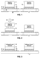
- Fig. 1 is a cross-sectional view of two LED dice 10 mounted on a package substrate 12.
- Each LED die 10 includes a sapphire growth substrate 14, n-type layers 16, an active layer 18, and p-type layers 20.
- the p-layer surface is highly doped to form an ohmic contact with a die metallization layer (e.g., NiAg). It is preferable if the metallization is highly reflective to light emitted by the active layer.
- the metallization layer is then bonded to a metal contact pad 22 on the package substrate 12.
- the bond technology may be solder, thermo compression, interdiffusion, or an Au stud bump array bonded by an ultrasonic weld.
- the combination of the die metallization and bond material is shown as metal 24 and may include a diffusion barrier or other layers to protect the optical properties of the metallization layer adjacent the p-layer 20.
- the LED dice 10 are typically from the same wafer but can, instead, be different types and colors.
- the package substrate 12 may be an array of package elements that will later be separated. Fig. 1 shows two package elements that will later be separated. Any arrangement of LEDs may be used such as arrays of LEDs or groups of arrays.
- the package substrate 12 may be formed of the electrically insulating material AIN, with gold contact pads 22 connected to solder able electrodes 26 using vias and/or metal traces.
- the package substrate 12 may be formed of a conducting material if passivated to prevent shorting, such as anodized AlSiC.
- the package substrate 12 is thermally conductive to act as a heat sink or to conduct heat to a larger heat sink.
- the LEDs may have a lens cap attached to them, or be coated with a phosphor (for converting blue or UV light to create a white light), or be further processed, and the package may be soldered to a printed circuit board, if appropriate for the particular application.
- a lens cap attached to them, or be coated with a phosphor (for converting blue or UV light to create a white light), or be further processed, and the package may be soldered to a printed circuit board, if appropriate for the particular application.
- Fig. 2 illustrates the growth substrate being removed using an excimer laser beam 30.
- the laser beam 30 melts the GaN material at its interface with the growth substrate, allowing the growth substrate to then be lifted off.
- Figs. 3 and 4 illustrate an alternative technique for growth substrate removal using etching.
- the growth substrate 32 may be silicon based (e.g., SiC, SiC-on-insulator, SiC-on-quartz, Si, etc.) so that it is etchable using conventional etching techniques, such as reactive ion etching (RIE).
- RIE reactive ion etching
- the etchant is shown as etchant 34.
- Additional non-laser liftoff techniques can be used to remove the growth substrate.
- a liftoff technique may etch away a layer between the growth substrate and the LED layers.
- the growth substrate may be SiCOI, and an etchant solution etches away the insulator material. The remainder of the growth substrate may then be lifted off.
- a sapphire substrate with an undercut etch layer may also be used.
- the growth substrate 32 may also be removed by lapping.
- the top surface of the package substrate 12 with the dice bonded thereto must be planar. Depositing a filler between the dice may serve to mechanically support the dice during the lapping process.
- An unusual aspect of the process described herein is that the LED-forming process is continued after the LED is mounted on the package substrate 12. In conventional designs, the LED is completely fabricated before being mounted on a support substrate.
- a wide array of semiconductor processing may be applied to the transferred LED layers in order to enhance optical extraction and establish electrical contact (for vertical injection devices only).
- the package substrate 12 must be protected from the effects of the processing. Note that precise placement ( ⁇ 2 microns) of the dice is typically necessary to allow reliable lithographic process steps.
- a protective layer 36 of, for example, polyimide is deposited to protect the package substrate 12 during subsequent processes, such as etching.
- the protective layer is removed from the top of the LED by a simple planarization step or mask/etch step.
- a thin ( ⁇ 15 micron) layer of UV transparent material e.g., aluminum oxide
- the lifting off the growth substrate would then lift off the aluminum oxide only over the growth substrate, providing a self-aligned protective layer for the package substrate 12. If the thickness of the transparent layer is approximately matched to the LED transferred layers, then planarization of the surface may be achieved.
- the exposed, relatively thick, GaN layer 16 is thinned by etching using a dry etch 38 such as RIE.
- the thickness of the GaN layer 16 being etched is 7 microns, and the etching reduces the thickness of the GaN layer 16 to approximately 1 micron. If the initial thickness of all the epitaxial LED layers is 9 microns, in this case the etching causes the total thickness of the LED layers to be 3 microns.
- the thinning process removes any damage caused by the laser lift off process, as well as reduces the thickness of the optically absorbing layers that are no longer needed, such as a low temperature GaN nucleation layer and adjacent layers. All or a portion of the n-type cladding layer adjacent to the active layer is left intact.
- planarization may be required to enable successful lithography.
- the structure is planarized in preparation for a metallization step. Planarization and top metallization is not needed if the LED is a flip-chip type, discussed with respect to Figs. 14 and 15. Planarization may be performed with a simple mechanical polishing step.
- a photoresist 40 is deposited.
- the photoresist is selectively exposed by UV radiation through a mask and developed to leave mask portions 42, where it is desired to contact the exposed n-layer 16 with metal.
- the subsequent metal layer may form fingers or another pattern to distribute the current while providing space for light to pass.
- the metal layer can be made very thin so as to be transparent.
- a transparent conductor such as indium tin oxide (ITO) may be employed to spread current.
- a metal 44 is deposited.
- the metal may be any conventional metal used in LEDs, such as Au, Ni, Ag, and combinations of metals for forming metal alloys.
- the metal may be deposited by sputtering or evaporation.
- a metal liftoff process is performed by dissolving the underlying photoresist and lifting off the metal.
- the metal layer(s) may be deposited first, and lithographic patterning of the metals can be achieved with metal etching using a photoresist mask.
- the light-emitting top surface of the LED is roughened for increased light extraction.
- layer 16 is photo-electrochemically etched using a KOH solution 46. This forms a "white" roughness in the GaN surface (having n-type Si doping). This etching process can be used to further thin the n-layer 16 and stop at a predetermined thickness using an etch stop layer grown during the LED formation process. This latter approach is useful for resonant device designs. For such devices, a mirror stack (e.g., a Bragg reflector) may now be deposited on the top surface of the LED. Additional light extraction techniques could include micron or nanometer scale patterned etching (dimple or photonic crystal). Forming patterns such a dimples or photonic crystals are well known.
- the protective layer 36 is then chemically removed.
- a phosphor material may be deposited over the LED die for wavelength shifting the light.
- the phosphor may be deposited using an electro-phoretic deposition (EPD) or screen-printing technique.
- a wire 48 is bonded to the top metal 44 and a package substrate contact pad 22.
- a rigid metal bridge 47 shown in Fig. 13B, may be deposited between the metal 44 and the pad 22.
- the resulting package substrate 12 is then diced using conventional techniques (e.g., scribe-and-break or sawing).
- Each package substrate die may contain one or more LEDs, either of the same color or of different colors.
- Each package substrate die may contain other circuitry, such as detectors, multiplexers, regulators, etc.
- the resulting package element may be further processed by, for example, receiving an LED lens cap, mounting on a printed circuit board, etc.
- the resulting package element of Fig. 13A or 13B has a very thin LED directly mounted on a package substrate that extends beyond the boundaries of the LED. No support substrate is required, thus eliminating the thermal and electrical resistance introduced by a support substrate. Since the LED is very thin, there is little optical absorption by the layers. Light extraction features may be provided in the top layer surface. In the case of roughening the surface, high surface randomization is provided, and photons generated within the epitaxial layers experience a high frequency of randomizing events. The short path length between events and the absence of absorbing regions of epitaxial material (e.g., the absence of a low-temperature GaN nucleation layer and adjacent high defect density regions) ensure a high light extraction efficiency.
- the resulting thin film (TF) LEDs are also advantageous for resonant structures such as resonant cavity and photonic-crystal based LEDs, since the reduced thickness of high refractive index material substantially reduces the number of optical modes and allows for designs with higher extraction efficiency and radiance.
- the distance between the primary emission surface (the top surface) and the package substrate surface is less than 50 microns, although typically the distance will be much less (e.g., 20 microns or less).
- the thickness of the LED layers may be 10 microns or less and typically less than 3 microns.
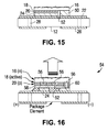
- Figs. 14 and 15 illustrate the use of a flip-chip LED 49 in the above-described packaging method.
- a flip-chip LED does not require any wire bond for contacting the n or p-layers so that it has a lower profile and is less fragile.
- all elements are the same as Fig. 1 except portions of the p-layer 20 and active layer 18 are etched away during the LED forming process, and metal 50 (metallization layer plus bonding metal) contacts the n-layer 16 on the same side as the p-contact metal 24.
- An under fill material 52 may be deposited in the voids beneath the LED to reduce thermal gradients across the LED, add mechanical strength to the attachment, and prevent contaminants from contacting the LED material. Since no top metal layer needs to be formed, the steps shown in Figs. 7-11 may be skipped.
- the n-metal 50 and p-metal 24 are bonded to the pads 22 on the package substrate 12.
- Fig. 16 illustrates a flip chip LED 54 where the metal electrode 56 for the n-layer 16 is formed in a pattern across the n-layer to distribute the current.
- the metal electrode 56 is insulated from the p-contact metallization 58 by an insulating material 60.
- the pattern of metal electrode 56 may be like fmgers, a polka dot pattern, or any other pattern. Non-contiguous metal patterns require an additional insulating and conducting layer to make contact to all the metal portions.
- An array of separated package substrates 12 are prepared by surrounding the metal bonding regions on each package substrate with regions that are not affected by the LED bonding process, such that the portion of the package substrate extending beyond the LED die of interest does not damage or become bonded to adjacent LED dies on the wafer during the bonding process.
- Methods to render areas unaffected by the bonding process include a reduced height or coating with an inert film such as SiO 2 .
- the wafer with the LEDs is placed in contact with a separated package substrate such that the first desired LED die is attached to the package substrate in a manner similar to the previously described method, using a combination of localized pressure, heat, and ultrasonic agitation.
- the separation of the growth substrate from the bonded device follows, using the laser lift off method, localized to the die area.
- An optical pathway through the device attachment system would be required for the laser beam.
- An additional advantage of this substrate-reuse technique is that the pulling force could be maintained on the device during the growth substrate separation, increasing the LED's capacity for absorbing thermal shock associated with laser liftoff.
- Fig. 17 is an exploded view of one embodiment of the package substrate 12 with an LED die 10 mounted in a package.
- a heat-sinking slug 60 is placed into an insert-molded lead frame 62.
- the insert-molded lead frame 62 is, for example, a filled plastic material molded around metal leads 64 that provide an electrical path.
- Slug 60 may include an optional reflector cup 66.
- the LED die 10 attached to the package substrate 12 is mounted directly or indirectly to slug 60.
- the metal leads 64 are bonded to the electrodes 26 (Fig. 13A) on the package substrate 12.
- An optical lens 68 may be added.
Landscapes
- Led Devices (AREA)
- Led Device Packages (AREA)
- Engineering & Computer Science (AREA)
- Microelectronics & Electronic Packaging (AREA)
Applications Claiming Priority (1)
| Application Number | Priority Date | Filing Date | Title |
|---|---|---|---|
| US10/977,294 US7256483B2 (en) | 2004-10-28 | 2004-10-28 | Package-integrated thin film LED |
Publications (3)
| Publication Number | Publication Date |
|---|---|
| EP1653523A2 true EP1653523A2 (de) | 2006-05-03 |
| EP1653523A3 EP1653523A3 (de) | 2009-02-11 |
| EP1653523B1 EP1653523B1 (de) | 2018-08-01 |
Family
ID=35709267
Family Applications (1)
| Application Number | Title | Priority Date | Filing Date |
|---|---|---|---|
| EP05110003.0A Expired - Lifetime EP1653523B1 (de) | 2004-10-28 | 2005-10-26 | Leuchtdioden-Verpackung |
Country Status (4)
| Country | Link |
|---|---|
| US (5) | US7256483B2 (de) |
| EP (1) | EP1653523B1 (de) |
| JP (1) | JP4885521B2 (de) |
| TW (1) | TWI413273B (de) |
Cited By (28)
| Publication number | Priority date | Publication date | Assignee | Title |
|---|---|---|---|---|
| WO2007001124A1 (en) | 2005-06-29 | 2007-01-04 | Seoul Opto Device Co., Ltd. | Light emitting diode having a thermal conductive substrate and method of fabricating the same |
| DE102007004303A1 (de) * | 2006-08-04 | 2008-02-07 | Osram Opto Semiconductors Gmbh | Dünnfilm-Halbleiterbauelement und Bauelement-Verbund |
| WO2009007886A1 (en) * | 2007-07-09 | 2009-01-15 | Koninklijke Philips Electronics N.V. | Substrate removal during led formation |
| WO2008112128A3 (en) * | 2007-03-08 | 2009-01-22 | Sensors For Med & Science Inc | Light emitting diode for harsh environments |
| WO2009077974A3 (en) * | 2007-12-14 | 2009-08-13 | Koninkl Philips Electronics Nv | Contact for a semiconductor light emitting device |
| WO2009132618A1 (de) * | 2008-04-29 | 2009-11-05 | Osram Opto Semiconductors Gmbh | Oberflächenmontierbares leuchtdioden-modul und verfahren zur herstellung eines oberflächenmontierbaren leuchtdioden-moduls |
| WO2009152790A1 (de) * | 2008-06-18 | 2009-12-23 | Osram Opto Semiconductors Gmbh | Strahlungsemittierendes bauelement und verfahren zur herstellung eines strahlungsemittierenden bauelements |
| WO2010034277A1 (de) * | 2008-09-29 | 2010-04-01 | Osram Opto Semiconductors Gmbh | Led-modul und herstellungsverfahren |
| WO2011082497A1 (en) * | 2010-01-11 | 2011-07-14 | Cooledge Lighting Inc. | Package for light emitting and receiving devices |
| EP2111651A4 (de) * | 2007-02-13 | 2011-08-17 | 3M Innovative Properties Co | Led mit linsen und verfahren zu ihrer herstellung |
| EP2262010A4 (de) * | 2008-04-24 | 2011-09-14 | Lg Innotek Co Ltd | Lichtemittierendes halbleiterbauelement |
| US8058147B2 (en) | 2005-08-05 | 2011-11-15 | Osram Opto Semiconductors Gmbh | Method for producing semiconductor components and thin-film semiconductor component |
| WO2012034764A1 (de) * | 2010-09-15 | 2012-03-22 | Osram Opto Semiconductors Gmbh | Galvanisch beschichtetes optoelektronisches halbleiterbauteil und verfahren zur herstellung eines optoelektronisches halbleiterbauteils |
| CN102738130A (zh) * | 2010-12-14 | 2012-10-17 | 英飞凌科技股份有限公司 | 管芯装置和形成管芯装置的方法 |
| US8338849B2 (en) | 2009-06-27 | 2012-12-25 | Cooledge Lighting, Inc. | High efficiency LEDS and LED lamps |
| US8384121B2 (en) | 2010-06-29 | 2013-02-26 | Cooledge Lighting Inc. | Electronic devices with yielding substrates |
| EP2074659A4 (de) * | 2006-09-08 | 2013-06-19 | Semi Photonics Co Ltd | Beschichtungsverfahren |
| WO2013105015A1 (en) * | 2012-01-12 | 2013-07-18 | Koninklijke Philips N.V. | Sidewall etching of led die to improve light extraction |
| US8653539B2 (en) | 2010-01-04 | 2014-02-18 | Cooledge Lighting, Inc. | Failure mitigation in arrays of light-emitting devices |
| RU2515205C2 (ru) * | 2008-09-24 | 2014-05-10 | Конинклейке Филипс Электроникс Н.В. | Полупроводниковые светоизлучающие устройства, выращенные на композитных подложках |
| US8877561B2 (en) | 2012-06-07 | 2014-11-04 | Cooledge Lighting Inc. | Methods of fabricating wafer-level flip chip device packages |
| US9142720B2 (en) | 2007-01-29 | 2015-09-22 | Osram Opto Semiconductors Gmbh | Thin-film light emitting diode chip and method for producing a thin-film light emitting diode chip |
| US9209059B2 (en) | 2009-12-17 | 2015-12-08 | Cooledge Lighting, Inc. | Method and eletrostatic transfer stamp for transferring semiconductor dice using electrostatic transfer printing techniques |
| CN105720141A (zh) * | 2016-03-11 | 2016-06-29 | 东莞市中镓半导体科技有限公司 | 一种无损伤的GaN衬底激光剥离方法 |
| US9480133B2 (en) | 2010-01-04 | 2016-10-25 | Cooledge Lighting Inc. | Light-emitting element repair in array-based lighting devices |
| EP3255742A1 (de) * | 2011-12-24 | 2017-12-13 | Princeton Optronics, Inc. | Überflächenmontageverpackung für hochgeschwindigkeits-senkrecht-oberflächenemissionslaser |
| EP2162928B1 (de) * | 2007-06-29 | 2018-04-11 | OSRAM Opto Semiconductors GmbH | Verfahren zur herstellung einer mehrzahl optoelektronischer bauelemente und optoelektronisches bauelement |
| US9944031B2 (en) | 2007-02-13 | 2018-04-17 | 3M Innovative Properties Company | Molded optical articles and methods of making same |
Families Citing this family (229)
| Publication number | Priority date | Publication date | Assignee | Title |
|---|---|---|---|---|
| US20070126016A1 (en) * | 2005-05-12 | 2007-06-07 | Epistar Corporation | Light emitting device and manufacture method thereof |
| US7456035B2 (en) * | 2003-07-29 | 2008-11-25 | Lumination Llc | Flip chip light emitting diode devices having thinned or removed substrates |
| FR2862424B1 (fr) * | 2003-11-18 | 2006-10-20 | Valeo Electronique Sys Liaison | Dispositif de refroidissement d'un composant electrique et procede de fabrication de ce dispositif |
| EP1706893A2 (de) * | 2003-12-24 | 2006-10-04 | Gelcore LLC | Laser-abhebung von saphir von einem nitrid-flipchip |
| US20070267646A1 (en) * | 2004-06-03 | 2007-11-22 | Philips Lumileds Lighting Company, Llc | Light Emitting Device Including a Photonic Crystal and a Luminescent Ceramic |
| US7361938B2 (en) | 2004-06-03 | 2008-04-22 | Philips Lumileds Lighting Company Llc | Luminescent ceramic for a light emitting device |
| JP4386191B2 (ja) * | 2004-12-15 | 2009-12-16 | セイコーエプソン株式会社 | 光素子 |
| TWI374553B (en) * | 2004-12-22 | 2012-10-11 | Panasonic Corp | Semiconductor light emitting device, illumination module, illumination apparatus, method for manufacturing semiconductor light emitting device, and method for manufacturing semiconductor light emitting element |
| US7524686B2 (en) * | 2005-01-11 | 2009-04-28 | Semileds Corporation | Method of making light emitting diodes (LEDs) with improved light extraction by roughening |
| US7646033B2 (en) * | 2005-01-11 | 2010-01-12 | Semileds Corporation | Systems and methods for producing white-light light emitting diodes |
| US8680534B2 (en) | 2005-01-11 | 2014-03-25 | Semileds Corporation | Vertical light emitting diodes (LED) having metal substrate and spin coated phosphor layer for producing white light |
| US7195944B2 (en) * | 2005-01-11 | 2007-03-27 | Semileds Corporation | Systems and methods for producing white-light emitting diodes |
| US20110284866A1 (en) * | 2005-01-11 | 2011-11-24 | Tran Chuong A | Light-emitting diode (led) structure having a wavelength-converting layer and method of producing |
| US7473936B2 (en) * | 2005-01-11 | 2009-01-06 | Semileds Corporation | Light emitting diodes (LEDs) with improved light extraction by roughening |
| US7563625B2 (en) * | 2005-01-11 | 2009-07-21 | SemiLEDs Optoelectronics Co., Ltd. | Method of making light-emitting diodes (LEDs) with improved light extraction by roughening |
| US20150295154A1 (en) | 2005-02-03 | 2015-10-15 | Epistar Corporation | Light emitting device and manufacturing method thereof |
| US9018655B2 (en) * | 2005-02-03 | 2015-04-28 | Epistar Corporation | Light emitting apparatus and manufacture method thereof |
| TWI244228B (en) * | 2005-02-03 | 2005-11-21 | United Epitaxy Co Ltd | Light emitting device and manufacture method thereof |
| US7932111B2 (en) * | 2005-02-23 | 2011-04-26 | Cree, Inc. | Substrate removal process for high light extraction LEDs |
| DE102005020908A1 (de) * | 2005-02-28 | 2006-08-31 | Osram Opto Semiconductors Gmbh | Beleuchtungsvorrichtung |
| DE112006001414A5 (de) * | 2005-05-30 | 2008-03-06 | Osram Opto Semiconductors Gmbh | Gehäusekörper und Verfahren zu dessen Herstellung |
| US7736945B2 (en) * | 2005-06-09 | 2010-06-15 | Philips Lumileds Lighting Company, Llc | LED assembly having maximum metal support for laser lift-off of growth substrate |
| US7754507B2 (en) * | 2005-06-09 | 2010-07-13 | Philips Lumileds Lighting Company, Llc | Method of removing the growth substrate of a semiconductor light emitting device |
| US20070069225A1 (en) * | 2005-09-27 | 2007-03-29 | Lumileds Lighting U.S., Llc | III-V light emitting device |
| US8334155B2 (en) * | 2005-09-27 | 2012-12-18 | Philips Lumileds Lighting Company Llc | Substrate for growing a III-V light emitting device |
| DE102006004591A1 (de) * | 2005-09-29 | 2007-04-05 | Osram Opto Semiconductors Gmbh | Strahlungsemittierender Halbleiterchip |
| US7718449B2 (en) * | 2005-10-28 | 2010-05-18 | Lumination Llc | Wafer level package for very small footprint and low profile white LED devices |
| WO2007081719A2 (en) | 2006-01-05 | 2007-07-19 | Illumitex, Inc. | Separate optical device for directing light from an led |
| WO2007148866A1 (en) * | 2006-06-23 | 2007-12-27 | Lg Electronics Inc. | Light emitting diode having vertical topology and method of making the same |
| US7843074B2 (en) * | 2006-09-12 | 2010-11-30 | Lumination Llc | Underfill for light emitting device |
| US9111950B2 (en) * | 2006-09-28 | 2015-08-18 | Philips Lumileds Lighting Company, Llc | Process for preparing a semiconductor structure for mounting |
| US8087960B2 (en) | 2006-10-02 | 2012-01-03 | Illumitex, Inc. | LED system and method |
| KR100826412B1 (ko) | 2006-11-03 | 2008-04-29 | 삼성전기주식회사 | 질화물 반도체 발광 소자 및 제조방법 |
| US8283683B2 (en) * | 2006-11-07 | 2012-10-09 | Opto Tech Corporation | Chip-bonding light emitting diode chip |
| TWI324403B (en) * | 2006-11-07 | 2010-05-01 | Opto Tech Corp | Light emitting diode and method manufacturing the same |
| KR20090088365A (ko) * | 2006-11-08 | 2009-08-19 | 씨. 아이. 카세이 가부시기가이샤 | 발광장치와 그 제조방법 |
| KR100867541B1 (ko) * | 2006-11-14 | 2008-11-06 | 삼성전기주식회사 | 수직형 발광 소자의 제조 방법 |
| US20080197369A1 (en) * | 2007-02-20 | 2008-08-21 | Cree, Inc. | Double flip semiconductor device and method for fabrication |
| US8409972B2 (en) * | 2007-04-11 | 2013-04-02 | Cree, Inc. | Light emitting diode having undoped and unintentionally doped nitride transition layer |
| DE102007022947B4 (de) | 2007-04-26 | 2022-05-05 | OSRAM Opto Semiconductors Gesellschaft mit beschränkter Haftung | Optoelektronischer Halbleiterkörper und Verfahren zur Herstellung eines solchen |
| GB2455489B (en) * | 2007-08-22 | 2012-05-30 | Photonstar Led Ltd | High thermal performance packaging for optoelectronics devices |
| KR101501307B1 (ko) * | 2007-09-21 | 2015-03-10 | 가부시끼가이샤 도시바 | 발광 장치 제작 방법 |
| TWI369009B (en) | 2007-09-21 | 2012-07-21 | Nat Univ Chung Hsing | Light-emitting chip device with high thermal conductivity |
| WO2009039233A1 (en) * | 2007-09-21 | 2009-03-26 | Bridgelux, Inc. | Light-emitting chip device with high thermal conductivity |
| TWI419355B (zh) * | 2007-09-21 | 2013-12-11 | Nat Univ Chung Hsing | 高光取出率的發光二極體晶片及其製造方法 |
| GB0721957D0 (en) * | 2007-11-08 | 2007-12-19 | Photonstar Led Ltd | Ultra high thermal performance packaging for optoelectronics devices |
| US9461201B2 (en) | 2007-11-14 | 2016-10-04 | Cree, Inc. | Light emitting diode dielectric mirror |
| US7846751B2 (en) * | 2007-11-19 | 2010-12-07 | Wang Nang Wang | LED chip thermal management and fabrication methods |
| US7985979B2 (en) | 2007-12-19 | 2011-07-26 | Koninklijke Philips Electronics, N.V. | Semiconductor light emitting device with light extraction structures |
| DE102007062046B4 (de) * | 2007-12-21 | 2023-09-07 | OSRAM Opto Semiconductors Gesellschaft mit beschränkter Haftung | Lichtemittierende Bauelementeanordnung, lichtemittierendes Bauelement sowie Verfahren zum Herstellen einer Mehrzahl von lichtemittierenden Bauelementen |
| US8217482B2 (en) * | 2007-12-21 | 2012-07-10 | Avago Technologies General Ip (Singapore) Pte. Ltd. | Infrared proximity sensor package with reduced crosstalk |
| CN100508231C (zh) * | 2008-01-31 | 2009-07-01 | 鹤山丽得电子实业有限公司 | 一种发光二极管及其制造方法 |
| JP2011512037A (ja) | 2008-02-08 | 2011-04-14 | イルミテックス, インコーポレイテッド | エミッタ層成形のためのシステムおよび方法 |
| CN100483762C (zh) * | 2008-02-25 | 2009-04-29 | 鹤山丽得电子实业有限公司 | 一种发光二极管器件的制造方法 |
| JP5175121B2 (ja) * | 2008-02-29 | 2013-04-03 | 晶元光電股▲ふん▼有限公司 | 半導体素子 |
| CN101257076B (zh) * | 2008-03-27 | 2011-03-23 | 鹤山丽得电子实业有限公司 | 发光二极管的制造方法 |
| US20090250713A1 (en) * | 2008-04-04 | 2009-10-08 | Philips Lumileds Lighting Company, Llc | Reflective Contact for a Semiconductor Light Emitting Device |
| DE102008021659A1 (de) * | 2008-04-30 | 2009-11-05 | Ledon Lighting Jennersdorf Gmbh | LED-Element mit Dünnschicht-Halbleiterbauelement auf Galliumnitrid-Basis |
| US9404197B2 (en) | 2008-07-07 | 2016-08-02 | Soraa, Inc. | Large area, low-defect gallium-containing nitride crystals, method of making, and method of use |
| US8143148B1 (en) | 2008-07-14 | 2012-03-27 | Soraa, Inc. | Self-aligned multi-dielectric-layer lift off process for laser diode stripes |
| US10147843B2 (en) * | 2008-07-24 | 2018-12-04 | Lumileds Llc | Semiconductor light emitting device including a window layer and a light-directing structure |
| US20100279437A1 (en) * | 2009-05-01 | 2010-11-04 | Koninklijke Philips Electronics N.V. | Controlling edge emission in package-free led die |
| US8236582B2 (en) * | 2008-07-24 | 2012-08-07 | Philips Lumileds Lighting Company, Llc | Controlling edge emission in package-free LED die |
| GB2458972B (en) * | 2008-08-05 | 2010-09-01 | Photonstar Led Ltd | Thermally optimised led chip-on-board module |
| US8058669B2 (en) * | 2008-08-28 | 2011-11-15 | Taiwan Semiconductor Manufacturing Company, Ltd. | Light-emitting diode integration scheme |
| WO2010029460A1 (en) | 2008-09-09 | 2010-03-18 | Philips Intellectual Property & Standards Gmbh | Contacting a device with a conductor |
| US8236583B2 (en) | 2008-09-10 | 2012-08-07 | Tsmc Solid State Lighting Ltd. | Method of separating light-emitting diode from a growth substrate |
| WO2010033792A1 (en) * | 2008-09-18 | 2010-03-25 | Lumenz Llc | Textured semiconductor light-emitting devices |
| JP5282503B2 (ja) * | 2008-09-19 | 2013-09-04 | 日亜化学工業株式会社 | 半導体発光素子 |
| EP2253988A1 (de) * | 2008-09-19 | 2010-11-24 | Christie Digital Systems USA, Inc. | Lichtintegrierer für mehr als eine Lampe |
| US9142714B2 (en) | 2008-10-09 | 2015-09-22 | Nitek, Inc. | High power ultraviolet light emitting diode with superlattice |
| TWI608760B (zh) | 2008-11-13 | 2017-12-11 | 行家光電有限公司 | 形成螢光粉轉換發光元件之方法 |
| US8406004B2 (en) * | 2008-12-09 | 2013-03-26 | Stats Chippac Ltd. | Integrated circuit packaging system and method of manufacture thereof |
| TW201034256A (en) | 2008-12-11 | 2010-09-16 | Illumitex Inc | Systems and methods for packaging light-emitting diode devices |
| US7883910B2 (en) * | 2009-02-03 | 2011-02-08 | Industrial Technology Research Institute | Light emitting diode structure, LED packaging structure using the same and method of forming the same |
| WO2010092972A1 (ja) | 2009-02-13 | 2010-08-19 | 電気化学工業株式会社 | Led発光素子用複合材料基板、その製造方法及びled発光素子 |
| KR100969146B1 (ko) * | 2009-02-18 | 2010-07-08 | 엘지이노텍 주식회사 | 반도체 발광소자 및 그 제조방법 |
| US8323996B2 (en) * | 2009-03-02 | 2012-12-04 | Infineon Technologies Ag | Semiconductor device |
| US8202741B2 (en) * | 2009-03-04 | 2012-06-19 | Koninklijke Philips Electronics N.V. | Method of bonding a semiconductor device using a compliant bonding structure |
| US20140175377A1 (en) * | 2009-04-07 | 2014-06-26 | Soraa, Inc. | Polarized white light devices using non-polar or semipolar gallium containing materials and transparent phosphors |
| TWI485879B (zh) * | 2009-04-09 | 2015-05-21 | 隆達電子股份有限公司 | 發光二極體晶片及其製造方法 |
| US8420999B2 (en) * | 2009-05-08 | 2013-04-16 | Avago Technologies Ecbu Ip (Singapore) Pte. Ltd. | Metal shield and housing for optical proximity sensor with increased resistance to mechanical deformation |
| US7989824B2 (en) * | 2009-06-03 | 2011-08-02 | Koninklijke Philips Electronics N.V. | Method of forming a dielectric layer on a semiconductor light emitting device |
| US7732231B1 (en) | 2009-06-03 | 2010-06-08 | Philips Lumileds Lighting Company, Llc | Method of forming a dielectric layer on a semiconductor light emitting device |
| US8957380B2 (en) * | 2009-06-30 | 2015-02-17 | Avago Technologies General Ip (Singapore) Pte. Ltd. | Infrared attenuating or blocking layer in optical proximity sensor |
| US8779361B2 (en) * | 2009-06-30 | 2014-07-15 | Avago Technologies General Ip (Singapore) Pte. Ltd. | Optical proximity sensor package with molded infrared light rejection barrier and infrared pass components |
| US9525093B2 (en) | 2009-06-30 | 2016-12-20 | Avago Technologies General Ip (Singapore) Pte. Ltd. | Infrared attenuating or blocking layer in optical proximity sensor |
| WO2011007874A1 (ja) | 2009-07-17 | 2011-01-20 | 電気化学工業株式会社 | Ledチップ接合体、ledパッケージ、及びledパッケージの製造方法 |
| KR20110008550A (ko) * | 2009-07-20 | 2011-01-27 | 삼성전자주식회사 | 발광 소자 및 그 제조 방법 |
| JP5789512B2 (ja) | 2009-07-31 | 2015-10-07 | 電気化学工業株式会社 | Led搭載用ウエハとその製造方法、及びそのウエハを用いたled搭載構造体 |
| US8153475B1 (en) * | 2009-08-18 | 2012-04-10 | Sorra, Inc. | Back-end processes for substrates re-use |
| US8585253B2 (en) | 2009-08-20 | 2013-11-19 | Illumitex, Inc. | System and method for color mixing lens array |
| US8449128B2 (en) | 2009-08-20 | 2013-05-28 | Illumitex, Inc. | System and method for a lens and phosphor layer |
| US8143608B2 (en) * | 2009-09-10 | 2012-03-27 | Avago Technologies Ecbu Ip (Singapore) Pte. Ltd. | Package-on-package (POP) optical proximity sensor |
| US8350216B2 (en) * | 2009-09-10 | 2013-01-08 | Avago Technologies Ecbu Ip (Singapore) Pte. Ltd. | Miniaturized optical proximity sensor |
| US8716665B2 (en) * | 2009-09-10 | 2014-05-06 | Avago Technologies General Ip (Singapore) Pte. Ltd. | Compact optical proximity sensor with ball grid array and windowed substrate |
| US8207554B2 (en) * | 2009-09-11 | 2012-06-26 | Soraa, Inc. | System and method for LED packaging |
| US9583678B2 (en) | 2009-09-18 | 2017-02-28 | Soraa, Inc. | High-performance LED fabrication |
| US8933644B2 (en) | 2009-09-18 | 2015-01-13 | Soraa, Inc. | LED lamps with improved quality of light |
| US9293644B2 (en) | 2009-09-18 | 2016-03-22 | Soraa, Inc. | Power light emitting diode and method with uniform current density operation |
| JP5534763B2 (ja) * | 2009-09-25 | 2014-07-02 | 株式会社東芝 | 半導体発光装置の製造方法及び半導体発光装置 |
| TWI403003B (zh) * | 2009-10-02 | 2013-07-21 | Chi Mei Lighting Tech Corp | 發光二極體及其製造方法 |
| US8630326B2 (en) | 2009-10-13 | 2014-01-14 | Skorpios Technologies, Inc. | Method and system of heterogeneous substrate bonding for photonic integration |
| US9923105B2 (en) | 2013-10-09 | 2018-03-20 | Skorpios Technologies, Inc. | Processing of a direct-bandgap chip after bonding to a silicon photonic device |
| US11181688B2 (en) | 2009-10-13 | 2021-11-23 | Skorpios Technologies, Inc. | Integration of an unprocessed, direct-bandgap chip into a silicon photonic device |
| KR101114047B1 (ko) * | 2009-10-22 | 2012-03-09 | 엘지이노텍 주식회사 | 발광소자 및 그 제조방법 |
| US8269245B1 (en) | 2009-10-30 | 2012-09-18 | Soraa, Inc. | Optical device with wavelength selective reflector |
| JP5414579B2 (ja) * | 2009-11-19 | 2014-02-12 | 株式会社東芝 | 半導体発光装置 |
| US9733357B2 (en) | 2009-11-23 | 2017-08-15 | Avago Technologies General Ip (Singapore) Pte. Ltd. | Infrared proximity sensor package with improved crosstalk isolation |
| KR101619832B1 (ko) * | 2009-11-30 | 2016-05-13 | 삼성전자주식회사 | 발광다이오드 패키지, 이를 구비한 발광다이오드 패키지 모듈과 그 제조 방법, 및 이를 구비한 헤드 램프 모듈과 그 제어 방법 |
| CN102097420B (zh) * | 2009-12-10 | 2014-08-20 | 鸿富锦精密工业(深圳)有限公司 | 发光二极管及其制造方法 |
| US20110151588A1 (en) * | 2009-12-17 | 2011-06-23 | Cooledge Lighting, Inc. | Method and magnetic transfer stamp for transferring semiconductor dice using magnetic transfer printing techniques |
| TWI492363B (zh) * | 2009-12-18 | 2015-07-11 | Hon Hai Prec Ind Co Ltd | 發光二極體及其製造方法 |
| WO2011073886A1 (en) | 2009-12-18 | 2011-06-23 | Koninklijke Philips Electronics N.V. | Substrate for a semiconductor light emitting device |
| TW201213134A (en) * | 2010-01-25 | 2012-04-01 | Illumitex Inc | Method for protecting optical devices during manufacture |
| US8905588B2 (en) | 2010-02-03 | 2014-12-09 | Sorra, Inc. | System and method for providing color light sources in proximity to predetermined wavelength conversion structures |
| US10147850B1 (en) | 2010-02-03 | 2018-12-04 | Soraa, Inc. | System and method for providing color light sources in proximity to predetermined wavelength conversion structures |
| JP5017399B2 (ja) * | 2010-03-09 | 2012-09-05 | 株式会社東芝 | 半導体発光装置および半導体発光装置の製造方法 |
| US8441020B2 (en) | 2010-03-10 | 2013-05-14 | Micron Technology, Inc. | Light emitting diode wafer-level package with self-aligning features |
| JP2011222724A (ja) * | 2010-04-08 | 2011-11-04 | Panasonic Electric Works Co Ltd | 発光装置およびその製造方法 |
| US8298863B2 (en) * | 2010-04-29 | 2012-10-30 | Texas Instruments Incorporated | TCE compensation for package substrates for reduced die warpage assembly |
| CN102237473B (zh) * | 2010-05-07 | 2015-03-11 | 展晶科技(深圳)有限公司 | 发光二极管及其制造方法 |
| CN102263187A (zh) * | 2010-05-31 | 2011-11-30 | 展晶科技(深圳)有限公司 | 发光二极管封装结构及其制造方法 |
| US8471282B2 (en) * | 2010-06-07 | 2013-06-25 | Koninklijke Philips Electronics N.V. | Passivation for a semiconductor light emitting device |
| US8313964B2 (en) | 2010-06-18 | 2012-11-20 | Soraa, Inc. | Singulation method and resulting device of thick gallium and nitrogen containing substrates |
| US9293678B2 (en) | 2010-07-15 | 2016-03-22 | Micron Technology, Inc. | Solid-state light emitters having substrates with thermal and electrical conductivity enhancements and method of manufacture |
| US8698166B2 (en) | 2010-07-16 | 2014-04-15 | Industrial Technology Research Institute | Light emitting chip package module and light emitting chip package structure and manufacturing method thereof |
| WO2012016377A1 (en) | 2010-08-03 | 2012-02-09 | Industrial Technology Research Institute | Light emitting diode chip, light emitting diode package structure, and method for forming the same |
| US9178107B2 (en) | 2010-08-03 | 2015-11-03 | Industrial Technology Research Institute | Wafer-level light emitting diode structure, light emitting diode chip, and method for forming the same |
| US20120056228A1 (en) * | 2010-09-07 | 2012-03-08 | Phostek, Inc. | Led chip modules, method for packaging the led chip modules, and moving fixture thereof |
| US8803452B2 (en) | 2010-10-08 | 2014-08-12 | Soraa, Inc. | High intensity light source |
| US8610161B2 (en) | 2010-10-28 | 2013-12-17 | Tsmc Solid State Lighting Ltd. | Light emitting diode optical emitter with transparent electrical connectors |
| KR101714049B1 (ko) * | 2010-10-29 | 2017-03-08 | 엘지이노텍 주식회사 | 발광 소자 패키지 |
| KR20130140048A (ko) * | 2010-11-02 | 2013-12-23 | 코닌클리케 필립스 엔.브이. | 향상된 추출 효율을 가진 발광 디바이스 |
| KR101194844B1 (ko) | 2010-11-15 | 2012-10-25 | 삼성전자주식회사 | 발광소자 및 그 제조방법 |
| US8597967B1 (en) | 2010-11-17 | 2013-12-03 | Soraa, Inc. | Method and system for dicing substrates containing gallium and nitrogen material |
| US8896235B1 (en) | 2010-11-17 | 2014-11-25 | Soraa, Inc. | High temperature LED system using an AC power source |
| US8541951B1 (en) | 2010-11-17 | 2013-09-24 | Soraa, Inc. | High temperature LED system using an AC power source |
| US9922967B2 (en) | 2010-12-08 | 2018-03-20 | Skorpios Technologies, Inc. | Multilevel template assisted wafer bonding |
| US8841597B2 (en) | 2010-12-27 | 2014-09-23 | Avago Technologies Ip (Singapore) Pte. Ltd. | Housing for optical proximity sensor |
| US8653542B2 (en) | 2011-01-13 | 2014-02-18 | Tsmc Solid State Lighting Ltd. | Micro-interconnects for light-emitting diodes |
| KR101761834B1 (ko) * | 2011-01-28 | 2017-07-27 | 서울바이오시스 주식회사 | 웨이퍼 레벨 발광 다이오드 패키지 및 그것을 제조하는 방법 |
| US8324835B2 (en) * | 2011-02-11 | 2012-12-04 | Soraa, Inc. | Modular LED lamp and manufacturing methods |
| US8525396B2 (en) * | 2011-02-11 | 2013-09-03 | Soraa, Inc. | Illumination source with direct die placement |
| US8643257B2 (en) | 2011-02-11 | 2014-02-04 | Soraa, Inc. | Illumination source with reduced inner core size |
| US10036544B1 (en) | 2011-02-11 | 2018-07-31 | Soraa, Inc. | Illumination source with reduced weight |
| KR20120092325A (ko) * | 2011-02-11 | 2012-08-21 | 서울옵토디바이스주식회사 | 광 결정 구조를 갖는 발광 다이오드 및 그것을 제조하는 방법 |
| US8618742B2 (en) * | 2011-02-11 | 2013-12-31 | Soraa, Inc. | Illumination source and manufacturing methods |
| JP2012174902A (ja) | 2011-02-22 | 2012-09-10 | Stanley Electric Co Ltd | 窒化物半導体発光素子の製造方法 |
| DE102011012928A1 (de) | 2011-03-03 | 2012-09-06 | Osram Opto Semiconductors Gmbh | Verfahren zur Herstellung eines Dünnfilm-Halbleiterkörpers und Dünnfilm-Halbleiterkörper |
| DE102011013821B4 (de) | 2011-03-14 | 2024-05-23 | OSRAM Opto Semiconductors Gesellschaft mit beschränkter Haftung | Verfahren zur Herstellung zumindest eines optoelektronischen Halbleiterchips |
| JP5681035B2 (ja) * | 2011-04-25 | 2015-03-04 | 電気化学工業株式会社 | Led光源パッケージ |
| JP5148729B2 (ja) * | 2011-05-16 | 2013-02-20 | 株式会社東芝 | 窒化物半導体素子の製造方法 |
| US8828757B2 (en) * | 2011-08-15 | 2014-09-09 | Epistar Corporation | Light-emitting device and method for manufacturing the same |
| US8686431B2 (en) | 2011-08-22 | 2014-04-01 | Soraa, Inc. | Gallium and nitrogen containing trilateral configuration for optical devices |
| US9646827B1 (en) | 2011-08-23 | 2017-05-09 | Soraa, Inc. | Method for smoothing surface of a substrate containing gallium and nitrogen |
| US8759127B2 (en) * | 2011-08-31 | 2014-06-24 | Toshiba Techno Center Inc. | Gold micromask for roughening to promote light extraction in an LED |
| DE102011112000B4 (de) | 2011-08-31 | 2023-11-30 | OSRAM Opto Semiconductors Gesellschaft mit beschränkter Haftung | Leuchtdiodenchip |
| TWI484660B (zh) * | 2011-08-31 | 2015-05-11 | Kabushiki Kaisya Toshiba | 提昇發光二極體內光萃取率的粗化製程之金微遮罩 |
| US9117941B2 (en) * | 2011-09-02 | 2015-08-25 | King Dragon International Inc. | LED package and method of the same |
| US20150001570A1 (en) * | 2011-09-02 | 2015-01-01 | King Dragon International Inc. | LED Package and Method of the Same |
| CN103797598A (zh) | 2011-09-13 | 2014-05-14 | 电气化学工业株式会社 | Led发光元件保持基板用包覆材料及其制造方法 |
| CN104040735B (zh) * | 2011-10-06 | 2017-08-25 | 皇家飞利浦有限公司 | 半导体发光器件的表面处理 |
| US8884517B1 (en) | 2011-10-17 | 2014-11-11 | Soraa, Inc. | Illumination sources with thermally-isolated electronics |
| KR20140096107A (ko) * | 2011-11-07 | 2014-08-04 | 더 실라나 그룹 피티와이 리미티드 | 절연기판 상의 반도체 구조 및 그 제조방법 |
| US8912025B2 (en) | 2011-11-23 | 2014-12-16 | Soraa, Inc. | Method for manufacture of bright GaN LEDs using a selective removal process |
| US20150228694A1 (en) * | 2011-12-20 | 2015-08-13 | The Silanna Group Pty, Ltd | Monolithically integrated CMOS and acoustic wave device |
| EP2803093B1 (de) | 2012-01-10 | 2019-06-26 | Lumileds Holding B.V. | Gesteuerte led-lichtausgabe durch selektive bereichsaufrauung |
| US8896010B2 (en) | 2012-01-24 | 2014-11-25 | Cooledge Lighting Inc. | Wafer-level flip chip device packages and related methods |
| US8907362B2 (en) | 2012-01-24 | 2014-12-09 | Cooledge Lighting Inc. | Light-emitting dies incorporating wavelength-conversion materials and related methods |
| WO2013112435A1 (en) | 2012-01-24 | 2013-08-01 | Cooledge Lighting Inc. | Light - emitting devices having discrete phosphor chips and fabrication methods |
| EP2810306B1 (de) * | 2012-02-02 | 2021-03-10 | Lumileds LLC | Herstellung von leuchtdioden mit variabler ausgangsleistung |
| KR20130102746A (ko) * | 2012-03-08 | 2013-09-23 | 삼성전자주식회사 | 발광 장치의 제조 방법 |
| CN110246941A (zh) | 2012-03-19 | 2019-09-17 | 亮锐控股有限公司 | 在硅衬底上生长的发光器件 |
| JP5992702B2 (ja) | 2012-03-21 | 2016-09-14 | スタンレー電気株式会社 | 半導体発光素子、および、車両用灯具、ならびに、半導体発光素子の製造方法 |
| JP5684751B2 (ja) | 2012-03-23 | 2015-03-18 | 株式会社東芝 | 半導体発光素子及びその製造方法 |
| KR20130132137A (ko) * | 2012-05-25 | 2013-12-04 | 삼성전자주식회사 | 반도체 발광소자 제조방법 |
| TWI469389B (zh) * | 2012-06-19 | 2015-01-11 | 隆達電子股份有限公司 | 垂直式固態發光元件之製程 |
| DE102012105619A1 (de) * | 2012-06-27 | 2014-01-02 | Osram Opto Semiconductors Gmbh | Optoelektronisches Bauelement und Verfahren zur Herstellung eines optoelektronischen Bauelements |
| JP6348491B2 (ja) | 2012-07-20 | 2018-06-27 | コーニンクレッカ フィリップス エヌ ヴェKoninklijke Philips N.V. | セラミック緑色蛍光体と保護された赤色蛍光体層とを有するled |
| US9337405B2 (en) | 2012-08-31 | 2016-05-10 | Nichia Corporation | Light emitting device and method for manufacturing the same |
| JP6089507B2 (ja) * | 2012-08-31 | 2017-03-08 | 日亜化学工業株式会社 | 発光装置およびその製造方法 |
| US8981534B2 (en) * | 2012-09-14 | 2015-03-17 | Tsmc Solid State Lighting Ltd. | Pre-cutting a back side of a silicon substrate for growing better III-V group compound layer on a front side of the substrate |
| CN104969099A (zh) | 2012-09-26 | 2015-10-07 | 8797625加拿大有限公司 | 多层光干涉滤片 |
| CN104781931A (zh) | 2012-11-07 | 2015-07-15 | 皇家飞利浦有限公司 | 波长转换的发光设备 |
| EP2917937B1 (de) | 2012-11-07 | 2016-11-16 | Koninklijke Philips N.V. | Verfahren zur herestellung einer licht emittierenden vorrichtung mit einem filter und einer schutzschicht |
| CN103840054A (zh) * | 2012-11-20 | 2014-06-04 | 展晶科技(深圳)有限公司 | 发光二极管芯片 |
| US9761763B2 (en) | 2012-12-21 | 2017-09-12 | Soraa, Inc. | Dense-luminescent-materials-coated violet LEDs |
| US9054235B2 (en) | 2013-01-22 | 2015-06-09 | Micron Technology, Inc. | Solid-state transducer devices with optically-transmissive carrier substrates and related systems, methods, and devices |
| KR101881446B1 (ko) * | 2013-01-25 | 2018-07-24 | 삼성전자주식회사 | 발광 소자 패키지의 제조 방법 |
| JP6068165B2 (ja) | 2013-01-29 | 2017-01-25 | スタンレー電気株式会社 | 半導体光学装置、および半導体光学装置の製造方法 |
| US9530930B2 (en) | 2013-01-29 | 2016-12-27 | Nanyang Technological University | Method of fabricating semiconductor devices |
| US9425359B2 (en) | 2013-02-04 | 2016-08-23 | Industrial Technology Research Institute | Light emitting diode |
| US9548424B2 (en) | 2013-02-04 | 2017-01-17 | Industrial Technology Research Institute | Light emitting diode |
| TWI557942B (zh) | 2013-02-04 | 2016-11-11 | 財團法人工業技術研究院 | 發光二極體 |
| US9178109B2 (en) | 2013-02-17 | 2015-11-03 | Tien Yang Wang | Semiconductor light-emitting device and method of manufacturing the same |
| KR101504331B1 (ko) | 2013-03-04 | 2015-03-19 | 삼성전자주식회사 | 발광소자 패키지 |
| JP6136649B2 (ja) | 2013-06-28 | 2017-05-31 | 日亜化学工業株式会社 | 発光素子及び発光装置 |
| JP2015028967A (ja) | 2013-07-30 | 2015-02-12 | 株式会社東芝 | 半導体発光素子及び発光装置 |
| US9410664B2 (en) | 2013-08-29 | 2016-08-09 | Soraa, Inc. | Circadian friendly LED light source |
| US10535685B2 (en) | 2013-12-02 | 2020-01-14 | The Regents Of The University Of Michigan | Fabrication of thin-film electronic devices with non-destructive wafer reuse |
| KR102323289B1 (ko) * | 2014-01-07 | 2021-11-08 | 루미리즈 홀딩 비.브이. | 인광체 변환기를 갖는 비접착식 발광 디바이스 |
| US9343443B2 (en) | 2014-02-05 | 2016-05-17 | Cooledge Lighting, Inc. | Light-emitting dies incorporating wavelength-conversion materials and related methods |
| KR102116986B1 (ko) | 2014-02-17 | 2020-05-29 | 삼성전자 주식회사 | 발광 다이오드 패키지 |
| KR102188500B1 (ko) | 2014-07-28 | 2020-12-09 | 삼성전자주식회사 | 발광다이오드 패키지 및 이를 이용한 조명장치 |
| WO2016027186A1 (en) * | 2014-08-19 | 2016-02-25 | Koninklijke Philips N.V. | Sapphire collector for reducing mechanical damage during die level laser lift-off |
| KR101552196B1 (ko) | 2014-11-07 | 2015-09-11 | 제이앤디써키트주식회사 | 발광 소자가 실장가능한 인쇄 회로 기판의 제조 방법 |
| US9705051B2 (en) | 2014-11-18 | 2017-07-11 | PlayNitride Inc. | Light emitting device |
| TWI557943B (zh) * | 2014-11-18 | 2016-11-11 | 錼創科技股份有限公司 | 發光元件的電極結構 |
| EP3266048B1 (de) | 2015-03-06 | 2019-10-02 | Koninklijke Philips N.V. | Verfahren zur befestigung von keramischen phosphorplatten auf den gussformen einer lichtemittierenden vorrichtung (led) unter verwendung einer sägefolie |
| TW201639203A (zh) * | 2015-04-17 | 2016-11-01 | 新世紀光電股份有限公司 | 發光裝置及應用其之發光模組 |
| JP6807334B2 (ja) * | 2015-05-13 | 2021-01-06 | ルミレッズ ホールディング ベーフェー | ダイレベルのリフトオフの最中におけるメカニカルダメージを低減するためのサファイアコレクタ |
| WO2016200739A1 (en) | 2015-06-09 | 2016-12-15 | Koninklijke Philips N.V. | Led fabrication using high-refractive-index adhesives |
| US9966260B1 (en) * | 2015-09-25 | 2018-05-08 | Apple Inc. | Surface modification process for laser application |
| US10749078B2 (en) | 2016-11-14 | 2020-08-18 | Seoul Viosys Co., Ltd. | Light emitting diode having side reflection layer |
| WO2018223391A1 (en) * | 2017-06-09 | 2018-12-13 | Goertek. Inc | Micro-led array transfer method, manufacturing method and display device |
| TWI633684B (zh) * | 2017-07-07 | 2018-08-21 | 寶力精密科技股份有限公司 | 微led結構及其製作方法 |
| US10559723B2 (en) | 2017-08-25 | 2020-02-11 | Rohm Co., Ltd. | Optical device |
| EP3698407A4 (de) * | 2017-10-19 | 2021-07-14 | Tectus Corporation | Ultradichter led-projektor |
| US20190198720A1 (en) * | 2017-12-22 | 2019-06-27 | Lumileds Llc | Particle systems and patterning for monolithic led arrays |
| US11283240B2 (en) * | 2018-01-09 | 2022-03-22 | Oepic Semiconductors, Inc. | Pillar confined backside emitting VCSEL |
| US11233377B2 (en) * | 2018-01-26 | 2022-01-25 | Oepic Semiconductors Inc. | Planarization of backside emitting VCSEL and method of manufacturing the same for array application |
| US10879420B2 (en) | 2018-07-09 | 2020-12-29 | University Of Iowa Research Foundation | Cascaded superlattice LED system |
| KR20200095210A (ko) * | 2019-01-31 | 2020-08-10 | 엘지전자 주식회사 | 반도체 발광 소자, 이의 제조 방법, 및 이를 포함하는 디스플레이 장치 |
| JP7775708B2 (ja) * | 2019-03-29 | 2025-11-26 | 三菱ケミカル株式会社 | GaN基板ウエハおよびGaN基板ウエハの製造方法 |
| US12426410B2 (en) * | 2019-08-28 | 2025-09-23 | Tslc Corporation | Semiconductor components and semiconductor structures and methods of fabrication |
| US20220375987A1 (en) * | 2019-09-11 | 2022-11-24 | Jade Bird Display (shanghai) Limited | Multi-color led pixel unit and micro-led display panel |
| TWI824688B (zh) * | 2022-08-31 | 2023-12-01 | 晶呈科技股份有限公司 | 晶粒封裝體的接合與轉移方法 |
| KR20240155583A (ko) * | 2023-04-20 | 2024-10-29 | 에스케이키파운드리 주식회사 | 반도체 다이 제조방법 |
Family Cites Families (26)
| Publication number | Priority date | Publication date | Assignee | Title |
|---|---|---|---|---|
| US5376580A (en) * | 1993-03-19 | 1994-12-27 | Hewlett-Packard Company | Wafer bonding of light emitting diode layers |
| TW289837B (de) * | 1994-01-18 | 1996-11-01 | Hwelett Packard Co | |
| DE19629920B4 (de) * | 1995-08-10 | 2006-02-02 | LumiLeds Lighting, U.S., LLC, San Jose | Licht-emittierende Diode mit einem nicht-absorbierenden verteilten Braggreflektor |
| US5940683A (en) * | 1996-01-18 | 1999-08-17 | Motorola, Inc. | LED display packaging with substrate removal and method of fabrication |
| US5779924A (en) * | 1996-03-22 | 1998-07-14 | Hewlett-Packard Company | Ordered interface texturing for a light emitting device |
| US6784463B2 (en) * | 1997-06-03 | 2004-08-31 | Lumileds Lighting U.S., Llc | III-Phospide and III-Arsenide flip chip light-emitting devices |
| EP0905797B1 (de) * | 1997-09-29 | 2010-02-10 | OSRAM Opto Semiconductors GmbH | Halbleiterlichtquelle und Verfahren zu ihrer Herstellung |
| JP3641122B2 (ja) * | 1997-12-26 | 2005-04-20 | ローム株式会社 | 半導体発光素子、半導体発光モジュール、およびこれらの製造方法 |
| US20010042866A1 (en) * | 1999-02-05 | 2001-11-22 | Carrie Carter Coman | Inxalygazn optical emitters fabricated via substrate removal |
| US6320206B1 (en) * | 1999-02-05 | 2001-11-20 | Lumileds Lighting, U.S., Llc | Light emitting devices having wafer bonded aluminum gallium indium nitride structures and mirror stacks |
| US6177359B1 (en) * | 1999-06-07 | 2001-01-23 | Agilent Technologies, Inc. | Method for detaching an epitaxial layer from one substrate and transferring it to another substrate |
| DE19925733C2 (de) * | 1999-06-07 | 2001-07-19 | Montan Tech Gmbh | Anordnung zum Messen von Verschiebungen im Gebirge |
| US6133589A (en) | 1999-06-08 | 2000-10-17 | Lumileds Lighting, U.S., Llc | AlGaInN-based LED having thick epitaxial layer for improved light extraction |
| TWI289944B (en) * | 2000-05-26 | 2007-11-11 | Osram Opto Semiconductors Gmbh | Light-emitting-diode-element with a light-emitting-diode-chip |
| US6525335B1 (en) * | 2000-11-06 | 2003-02-25 | Lumileds Lighting, U.S., Llc | Light emitting semiconductor devices including wafer bonded heterostructures |
| US6791119B2 (en) * | 2001-02-01 | 2004-09-14 | Cree, Inc. | Light emitting diodes including modifications for light extraction |
| JP4122743B2 (ja) * | 2001-09-19 | 2008-07-23 | 松下電工株式会社 | 発光装置 |
| KR101030068B1 (ko) * | 2002-07-08 | 2011-04-19 | 니치아 카가쿠 고교 가부시키가이샤 | 질화물 반도체 소자의 제조방법 및 질화물 반도체 소자 |
| US20040104395A1 (en) * | 2002-11-28 | 2004-06-03 | Shin-Etsu Handotai Co., Ltd. | Light-emitting device, method of fabricating the same, and OHMIC electrode structure for semiconductor device |
| US20040259279A1 (en) * | 2003-04-15 | 2004-12-23 | Erchak Alexei A. | Light emitting device methods |
| US6831302B2 (en) * | 2003-04-15 | 2004-12-14 | Luminus Devices, Inc. | Light emitting devices with improved extraction efficiency |
| US6847057B1 (en) * | 2003-08-01 | 2005-01-25 | Lumileds Lighting U.S., Llc | Semiconductor light emitting devices |
| JP2005252222A (ja) * | 2004-02-03 | 2005-09-15 | Matsushita Electric Ind Co Ltd | 半導体発光装置、照明モジュール、照明装置、表示素子、および半導体発光装置の製造方法 |
| US20050236636A1 (en) * | 2004-04-23 | 2005-10-27 | Supernova Optoelectronics Corp. | GaN-based light-emitting diode structure |
| US6956246B1 (en) * | 2004-06-03 | 2005-10-18 | Lumileds Lighting U.S., Llc | Resonant cavity III-nitride light emitting devices fabricated by growth substrate removal |
| US7352006B2 (en) * | 2004-09-28 | 2008-04-01 | Goldeneye, Inc. | Light emitting diodes exhibiting both high reflectivity and high light extraction |
-
2004
- 2004-10-28 US US10/977,294 patent/US7256483B2/en not_active Expired - Lifetime
-
2005
- 2005-10-26 EP EP05110003.0A patent/EP1653523B1/de not_active Expired - Lifetime
- 2005-10-27 TW TW094137652A patent/TWI413273B/zh not_active IP Right Cessation
- 2005-10-28 JP JP2005342796A patent/JP4885521B2/ja not_active Expired - Lifetime
-
2006
- 2006-05-31 US US11/421,350 patent/US7488621B2/en not_active Expired - Lifetime
-
2009
- 2009-02-09 US US12/368,213 patent/US7875533B2/en not_active Expired - Lifetime
-
2010
- 2010-12-16 US US12/969,709 patent/US8455913B2/en not_active Expired - Lifetime
-
2013
- 2013-06-03 US US13/908,003 patent/US20130313562A1/en not_active Abandoned
Cited By (65)
| Publication number | Priority date | Publication date | Assignee | Title |
|---|---|---|---|---|
| EP1905103A4 (de) * | 2005-06-29 | 2011-01-19 | Seoul Opto Device Co Ltd | Leuchtdiode mit einem thermisch leitfähigen substrat und herstellungsverfahren dafür |
| WO2007001124A1 (en) | 2005-06-29 | 2007-01-04 | Seoul Opto Device Co., Ltd. | Light emitting diode having a thermal conductive substrate and method of fabricating the same |
| US8129207B2 (en) | 2005-06-29 | 2012-03-06 | Seoul Opto Device Co., Ltd. | Light emitting diode having a thermal conductive substrate and method of fabricating the same |
| US8039846B2 (en) | 2005-06-29 | 2011-10-18 | Seoul Opto Device Co., Ltd. | Light emitting diode having a thermal conductive substrate and method of fabricating the same |
| US8058147B2 (en) | 2005-08-05 | 2011-11-15 | Osram Opto Semiconductors Gmbh | Method for producing semiconductor components and thin-film semiconductor component |
| DE102007004303A1 (de) * | 2006-08-04 | 2008-02-07 | Osram Opto Semiconductors Gmbh | Dünnfilm-Halbleiterbauelement und Bauelement-Verbund |
| US8872330B2 (en) | 2006-08-04 | 2014-10-28 | Osram Opto Semiconductors Gmbh | Thin-film semiconductor component and component assembly |
| EP2074659A4 (de) * | 2006-09-08 | 2013-06-19 | Semi Photonics Co Ltd | Beschichtungsverfahren |
| US9142720B2 (en) | 2007-01-29 | 2015-09-22 | Osram Opto Semiconductors Gmbh | Thin-film light emitting diode chip and method for producing a thin-film light emitting diode chip |
| US9944031B2 (en) | 2007-02-13 | 2018-04-17 | 3M Innovative Properties Company | Molded optical articles and methods of making same |
| EP2111651A4 (de) * | 2007-02-13 | 2011-08-17 | 3M Innovative Properties Co | Led mit linsen und verfahren zu ihrer herstellung |
| US8330176B2 (en) | 2007-02-13 | 2012-12-11 | 3M Innovative Properties Company | LED devices having lenses and methods of making same |
| US7939832B2 (en) | 2007-03-08 | 2011-05-10 | Sensors For Medicine And Science, Inc. | Light emitting diode for harsh environments |
| US8415184B2 (en) | 2007-03-08 | 2013-04-09 | Sensors For Medicine And Science, Inc. | Light emitting diode for harsh environments |
| WO2008112128A3 (en) * | 2007-03-08 | 2009-01-22 | Sensors For Med & Science Inc | Light emitting diode for harsh environments |
| US8648356B2 (en) | 2007-03-08 | 2014-02-11 | Senseonics, Incorporated | Light emitting diode for harsh environments |
| EP2162928B1 (de) * | 2007-06-29 | 2018-04-11 | OSRAM Opto Semiconductors GmbH | Verfahren zur herstellung einer mehrzahl optoelektronischer bauelemente und optoelektronisches bauelement |
| US7867793B2 (en) | 2007-07-09 | 2011-01-11 | Koninklijke Philips Electronics N.V. | Substrate removal during LED formation |
| WO2009007886A1 (en) * | 2007-07-09 | 2009-01-15 | Koninklijke Philips Electronics N.V. | Substrate removal during led formation |
| US8679869B2 (en) | 2007-12-14 | 2014-03-25 | Philips Lumileds Lighting Company, Llc | Contact for a semiconductor light emitting device |
| WO2009077974A3 (en) * | 2007-12-14 | 2009-08-13 | Koninkl Philips Electronics Nv | Contact for a semiconductor light emitting device |
| RU2491683C2 (ru) * | 2007-12-14 | 2013-08-27 | Конинклейке Филипс Электроникс Н.В. | Контакт для полупроводникового светоизлучающего устройства |
| EP2657996A3 (de) * | 2008-04-24 | 2014-03-05 | LG Innotek Co., Ltd. | Lichtemittierendes Halbleiterbauelement |
| US8492782B2 (en) | 2008-04-24 | 2013-07-23 | Lg Innotek Co., Ltd. | Semiconductor light emitting device |
| EP2262010A4 (de) * | 2008-04-24 | 2011-09-14 | Lg Innotek Co Ltd | Lichtemittierendes halbleiterbauelement |
| WO2009132618A1 (de) * | 2008-04-29 | 2009-11-05 | Osram Opto Semiconductors Gmbh | Oberflächenmontierbares leuchtdioden-modul und verfahren zur herstellung eines oberflächenmontierbaren leuchtdioden-moduls |
| DE102008021402B4 (de) | 2008-04-29 | 2023-08-10 | OSRAM Opto Semiconductors Gesellschaft mit beschränkter Haftung | Oberflächenmontierbares Leuchtdioden-Modul und Verfahren zur Herstellung eines oberflächenmontierbaren Leuchtdioden-Moduls |
| WO2009152790A1 (de) * | 2008-06-18 | 2009-12-23 | Osram Opto Semiconductors Gmbh | Strahlungsemittierendes bauelement und verfahren zur herstellung eines strahlungsemittierenden bauelements |
| RU2515205C2 (ru) * | 2008-09-24 | 2014-05-10 | Конинклейке Филипс Электроникс Н.В. | Полупроводниковые светоизлучающие устройства, выращенные на композитных подложках |
| WO2010034277A1 (de) * | 2008-09-29 | 2010-04-01 | Osram Opto Semiconductors Gmbh | Led-modul und herstellungsverfahren |
| US10910522B2 (en) | 2009-06-27 | 2021-02-02 | Cooledge Lighting Inc. | High efficiency LEDs and LED lamps |
| US9966414B2 (en) | 2009-06-27 | 2018-05-08 | Cooledge Lighting Inc. | High efficiency LEDs and LED lamps |
| US10281091B2 (en) | 2009-06-27 | 2019-05-07 | Cooledge Lighting Inc. | High efficiency LEDs and LED lamps |
| US8338849B2 (en) | 2009-06-27 | 2012-12-25 | Cooledge Lighting, Inc. | High efficiency LEDS and LED lamps |
| US8384114B2 (en) | 2009-06-27 | 2013-02-26 | Cooledge Lighting Inc. | High efficiency LEDs and LED lamps |
| US11415272B2 (en) | 2009-06-27 | 2022-08-16 | Cooledge Lighting, Inc. | High efficiency LEDs and LED lamps |
| US9765936B2 (en) | 2009-06-27 | 2017-09-19 | Cooledge Lighting Inc. | High efficiency LEDs and LED lamps |
| US9559150B2 (en) | 2009-06-27 | 2017-01-31 | Cooledge Lighting Inc. | High efficiency LEDs and LED lamps |
| US9431462B2 (en) | 2009-06-27 | 2016-08-30 | Cooledge Lighting, Inc. | High efficiency LEDs and LED lamps |
| US9179510B2 (en) | 2009-06-27 | 2015-11-03 | Cooledge Lighting Inc. | High efficiency LEDs and LED lamps |
| US9209059B2 (en) | 2009-12-17 | 2015-12-08 | Cooledge Lighting, Inc. | Method and eletrostatic transfer stamp for transferring semiconductor dice using electrostatic transfer printing techniques |
| US9107272B2 (en) | 2010-01-04 | 2015-08-11 | Cooledge Lighting Inc. | Failure mitigation in arrays of light-emitting devices |
| US9480133B2 (en) | 2010-01-04 | 2016-10-25 | Cooledge Lighting Inc. | Light-emitting element repair in array-based lighting devices |
| US8653539B2 (en) | 2010-01-04 | 2014-02-18 | Cooledge Lighting, Inc. | Failure mitigation in arrays of light-emitting devices |
| US8860318B2 (en) | 2010-01-04 | 2014-10-14 | Cooledge Lighting Inc. | Failure mitigation in arrays of light-emitting devices |
| WO2011082497A1 (en) * | 2010-01-11 | 2011-07-14 | Cooledge Lighting Inc. | Package for light emitting and receiving devices |
| US8907370B2 (en) | 2010-06-29 | 2014-12-09 | Cooledge Lighting Inc. | Electronic devices with yielding substrates |
| US8680567B2 (en) | 2010-06-29 | 2014-03-25 | Cooledge Lighting Inc. | Electronic devices with yielding substrates |
| US9252373B2 (en) | 2010-06-29 | 2016-02-02 | Cooledge Lighting, Inc. | Electronic devices with yielding substrates |
| US8466488B2 (en) | 2010-06-29 | 2013-06-18 | Cooledge Lighting Inc. | Electronic devices with yielding substrates |
| US9426860B2 (en) | 2010-06-29 | 2016-08-23 | Cooledge Lighting, Inc. | Electronic devices with yielding substrates |
| US8384121B2 (en) | 2010-06-29 | 2013-02-26 | Cooledge Lighting Inc. | Electronic devices with yielding substrates |
| US9054290B2 (en) | 2010-06-29 | 2015-06-09 | Cooledge Lighting Inc. | Electronic devices with yielding substrates |
| CN103140948A (zh) * | 2010-09-15 | 2013-06-05 | 欧司朗光电半导体有限公司 | 电镀覆层的光电子半导体组件和用于制造光电子半导体组件的方法 |
| WO2012034764A1 (de) * | 2010-09-15 | 2012-03-22 | Osram Opto Semiconductors Gmbh | Galvanisch beschichtetes optoelektronisches halbleiterbauteil und verfahren zur herstellung eines optoelektronisches halbleiterbauteils |
| US9041020B2 (en) | 2010-09-15 | 2015-05-26 | Osram Opto Semiconductors Gmbh | Electrolytically coated optoelectronic semiconductor component and method for producing an optoelectronic semiconductor component |
| CN102738130A (zh) * | 2010-12-14 | 2012-10-17 | 英飞凌科技股份有限公司 | 管芯装置和形成管芯装置的方法 |
| CN102738130B (zh) * | 2010-12-14 | 2015-05-20 | 英飞凌科技股份有限公司 | 管芯装置和形成管芯装置的方法 |
| EP3255742A1 (de) * | 2011-12-24 | 2017-12-13 | Princeton Optronics, Inc. | Überflächenmontageverpackung für hochgeschwindigkeits-senkrecht-oberflächenemissionslaser |
| WO2013105015A1 (en) * | 2012-01-12 | 2013-07-18 | Koninklijke Philips N.V. | Sidewall etching of led die to improve light extraction |
| US9214615B2 (en) | 2012-06-07 | 2015-12-15 | Cooledge Lighting Inc. | Methods of fabricating wafer-level flip chip device packages |
| US8877561B2 (en) | 2012-06-07 | 2014-11-04 | Cooledge Lighting Inc. | Methods of fabricating wafer-level flip chip device packages |
| US9231178B2 (en) | 2012-06-07 | 2016-01-05 | Cooledge Lighting, Inc. | Wafer-level flip chip device packages and related methods |
| CN105720141B (zh) * | 2016-03-11 | 2019-01-29 | 东莞市中镓半导体科技有限公司 | 一种无损伤的GaN衬底激光剥离方法 |
| CN105720141A (zh) * | 2016-03-11 | 2016-06-29 | 东莞市中镓半导体科技有限公司 | 一种无损伤的GaN衬底激光剥离方法 |
Also Published As
| Publication number | Publication date |
|---|---|
| US20060091409A1 (en) | 2006-05-04 |
| US20060240585A1 (en) | 2006-10-26 |
| US8455913B2 (en) | 2013-06-04 |
| EP1653523A3 (de) | 2009-02-11 |
| EP1653523B1 (de) | 2018-08-01 |
| TW200629605A (en) | 2006-08-16 |
| JP4885521B2 (ja) | 2012-02-29 |
| US20130313562A1 (en) | 2013-11-28 |
| US20100041170A1 (en) | 2010-02-18 |
| US7488621B2 (en) | 2009-02-10 |
| US7875533B2 (en) | 2011-01-25 |
| TWI413273B (zh) | 2013-10-21 |
| JP2006128710A (ja) | 2006-05-18 |
| US20110084301A1 (en) | 2011-04-14 |
| US7256483B2 (en) | 2007-08-14 |
Similar Documents
| Publication | Publication Date | Title |
|---|---|---|
| US7488621B2 (en) | Package-integrated thin film LED | |
| EP2308107B1 (de) | Halbleiterlichtemissionsvorrichtung mit einer fensterschicht und einer lichtleitenden struktur | |
| TWI663749B (zh) | 發光裝置及其製作方法 | |
| EP1417722B1 (de) | Flip-chip bonden von licht-emittierenden chips | |
| TWI422044B (zh) | 封裝發光裝置之晶片尺度方法及經晶片尺度封裝之發光裝置 | |
| US7329905B2 (en) | Chip-scale methods for packaging light emitting devices and chip-scale packaged light emitting devices | |
| JP2012060182A (ja) | 増加発光能力を持つiii族窒化物ledの製造方法 | |
| KR100878326B1 (ko) | 칩스케일 패키징 발광소자 및 그의 제조방법 | |
| CN106159073A (zh) | 发光元件及其制造方法 | |
| JP2004319685A (ja) | 半導体発光素子および半導体発光装置 |
Legal Events
| Date | Code | Title | Description |
|---|---|---|---|
| PUAI | Public reference made under article 153(3) epc to a published international application that has entered the european phase |
Free format text: ORIGINAL CODE: 0009012 |
|
| AK | Designated contracting states |
Kind code of ref document: A2 Designated state(s): AT BE BG CH CY CZ DE DK EE ES FI FR GB GR HU IE IS IT LI LT LU LV MC NL PL PT RO SE SI SK TR |
|
| AX | Request for extension of the european patent |
Extension state: AL BA HR MK YU |
|
| RAP1 | Party data changed (applicant data changed or rights of an application transferred) |
Owner name: PHILIPS LUMILEDS LIGHTING COMPANY LLC |
|
| PUAL | Search report despatched |
Free format text: ORIGINAL CODE: 0009013 |
|
| AK | Designated contracting states |
Kind code of ref document: A3 Designated state(s): AT BE BG CH CY CZ DE DK EE ES FI FR GB GR HU IE IS IT LI LT LU LV MC NL PL PT RO SE SI SK TR |
|
| AX | Request for extension of the european patent |
Extension state: AL BA HR MK YU |
|
| 17P | Request for examination filed |
Effective date: 20090811 |
|
| 17Q | First examination report despatched |
Effective date: 20090907 |
|
| AKX | Designation fees paid |
Designated state(s): DE |
|
| RBV | Designated contracting states (corrected) |
Designated state(s): DE FR GB |
|
| RAP1 | Party data changed (applicant data changed or rights of an application transferred) |
Owner name: LUMILEDS HOLDING B.V. |
|
| GRAP | Despatch of communication of intention to grant a patent |
Free format text: ORIGINAL CODE: EPIDOSNIGR1 |
|
| RIC1 | Information provided on ipc code assigned before grant |
Ipc: H01L 33/22 20100101ALN20180419BHEP Ipc: H01L 33/00 20060101AFI20180419BHEP Ipc: H01L 23/00 20060101ALN20180419BHEP Ipc: H01L 33/48 20100101ALI20180419BHEP |
|
| INTG | Intention to grant announced |
Effective date: 20180514 |
|
| GRAS | Grant fee paid |
Free format text: ORIGINAL CODE: EPIDOSNIGR3 |
|
| GRAA | (expected) grant |
Free format text: ORIGINAL CODE: 0009210 |
|
| AK | Designated contracting states |
Kind code of ref document: B1 Designated state(s): DE FR GB |
|
| REG | Reference to a national code |
Ref country code: GB Ref legal event code: FG4D |
|
| REG | Reference to a national code |
Ref country code: DE Ref legal event code: R096 Ref document number: 602005054344 Country of ref document: DE |
|
| REG | Reference to a national code |
Ref country code: FR Ref legal event code: PLFP Year of fee payment: 14 |
|
| RAP2 | Party data changed (patent owner data changed or rights of a patent transferred) |
Owner name: LUMILEDS HOLDING B.V. |
|
| REG | Reference to a national code |
Ref country code: DE Ref legal event code: R097 Ref document number: 602005054344 Country of ref document: DE |
|
| PLBE | No opposition filed within time limit |
Free format text: ORIGINAL CODE: 0009261 |
|
| STAA | Information on the status of an ep patent application or granted ep patent |
Free format text: STATUS: NO OPPOSITION FILED WITHIN TIME LIMIT |
|
| 26N | No opposition filed |
Effective date: 20190503 |
|
| P01 | Opt-out of the competence of the unified patent court (upc) registered |
Effective date: 20230530 |
|
| REG | Reference to a national code |
Ref country code: DE Ref legal event code: R079 Ref document number: 602005054344 Country of ref document: DE Free format text: PREVIOUS MAIN CLASS: H01L0033000000 Ipc: H10H0020000000 |
|
| PGFP | Annual fee paid to national office [announced via postgrant information from national office to epo] |
Ref country code: DE Payment date: 20241029 Year of fee payment: 20 |
|
| PGFP | Annual fee paid to national office [announced via postgrant information from national office to epo] |
Ref country code: GB Payment date: 20241022 Year of fee payment: 20 |
|
| PGFP | Annual fee paid to national office [announced via postgrant information from national office to epo] |
Ref country code: FR Payment date: 20241025 Year of fee payment: 20 |
|
| REG | Reference to a national code |
Ref country code: DE Ref legal event code: R071 Ref document number: 602005054344 Country of ref document: DE |
|
| REG | Reference to a national code |
Ref country code: GB Ref legal event code: PE20 Expiry date: 20251025 |