EP1653610B1 - Automatische Verstärkungsregelung mit Regelschleifeverstärkungssteuerung - Google Patents
Automatische Verstärkungsregelung mit Regelschleifeverstärkungssteuerung Download PDFInfo
- Publication number
- EP1653610B1 EP1653610B1 EP05256790A EP05256790A EP1653610B1 EP 1653610 B1 EP1653610 B1 EP 1653610B1 EP 05256790 A EP05256790 A EP 05256790A EP 05256790 A EP05256790 A EP 05256790A EP 1653610 B1 EP1653610 B1 EP 1653610B1
- Authority
- EP
- European Patent Office
- Prior art keywords
- signal
- power
- gain
- module
- received
- Prior art date
- Legal status (The legal status is an assumption and is not a legal conclusion. Google has not performed a legal analysis and makes no representation as to the accuracy of the status listed.)
- Ceased
Links
- 238000004891 communication Methods 0.000 claims description 27
- 238000000034 method Methods 0.000 claims description 8
- 230000000694 effects Effects 0.000 claims description 5
- 238000005259 measurement Methods 0.000 claims description 3
- 230000003111 delayed effect Effects 0.000 claims 1
- 238000001514 detection method Methods 0.000 claims 1
- 230000008859 change Effects 0.000 description 16
- 238000010586 diagram Methods 0.000 description 4
- 230000004044 response Effects 0.000 description 4
- 230000002452 interceptive effect Effects 0.000 description 3
- 230000007246 mechanism Effects 0.000 description 3
- 238000012545 processing Methods 0.000 description 3
- 238000012935 Averaging Methods 0.000 description 2
- 230000003321 amplification Effects 0.000 description 2
- 238000001914 filtration Methods 0.000 description 2
- 238000003199 nucleic acid amplification method Methods 0.000 description 2
- 230000008569 process Effects 0.000 description 2
- 230000009467 reduction Effects 0.000 description 2
- 238000013459 approach Methods 0.000 description 1
- 230000007423 decrease Effects 0.000 description 1
- 230000003247 decreasing effect Effects 0.000 description 1
- 230000001419 dependent effect Effects 0.000 description 1
- 238000005516 engineering process Methods 0.000 description 1
- 238000012986 modification Methods 0.000 description 1
- 230000004048 modification Effects 0.000 description 1
- 238000004088 simulation Methods 0.000 description 1
Images


Classifications
-
- H—ELECTRICITY
- H03—ELECTRONIC CIRCUITRY
- H03G—CONTROL OF AMPLIFICATION
- H03G3/00—Gain control in amplifiers or frequency changers
- H03G3/20—Automatic control
- H03G3/30—Automatic control in amplifiers having semiconductor devices
- H03G3/3052—Automatic control in amplifiers having semiconductor devices in bandpass amplifiers (H.F. or I.F.) or in frequency-changers used in a (super)heterodyne receiver
- H03G3/3068—Circuits generating control signals for both R.F. and I.F. stages
Definitions
- This invention relates to automatic gain control (AGC) Loop circuits, usually referred to as AGC loops because automatic gain control necessarily requires a feedback loop of some kind.
- AGC loops are used in communication systems to improve receiver operation by varying the gain applied to received signals based upon their detected power.
- AGC loops are needed in most communication systems because, as a practical matter, received signals are always subject to variations in power. The task of gain control is further complicated by the presence of interfering signals.
- first-order AGC loops are a basic characteristic of feedback control loops in general, not just AGC loops, and refers to the number of mathematical integrators in the loop.
- First-order loops are less complex and are known for their stability, i.e., their ability to converge on a desired steady-state signal value relatively quickly when there is a change in the received signal strength. For certain received signal conditions, however, first-order loops may not perform as well as desired, and in particular may not react fast enough to large or small received signal changes. First order loops are optimized either for speed or accuracy in performance.
- an AGC loop that has the stability of a first-order loop but also has the ability to react rapidly in the presence of large signal changes, interference signals, or in a frequency-hopping communications environment.
- the present invention is directed to these goals.
- EP-A-1 164 788 provides a digital broadcast receiving apparatus for amplifying a received modulated digital signal wave with automatically adjusted gain and demodulating the modulated signal wave to a digital signal.
- a tuner frequency converts the modulated digital signal wave to generate a first modulated signal.
- a first automatic gain control amplification unit controls gain of the tuner to make a level of the first modulated signal at a first predetermined level,
- An analog to digital converter converts the first modulated signal into a second modulated signal.
- a demodulator demodulates the second modulated signal to generate a first demodulated digital signal.
- a second automatic gain control amplifier generates a second demodulated digital signet where frequency fluctuations included in the digital modulated wave are eliminated.
- US Patent 5627857 discloses a linear, digital AGC in a radio.
- a received signal is demodulated to provide I and Q digital baseband signals.
- a received signal strength indication is determined from these signals and the resulting digital signal is adjusted to provide a logarithmic response. This signal is then integrated to provide a digital receive AGC adjust signal.
- An apparatus and method are provided for an automatic gain control (AGC) device (42), as recited in Claims 1 and 5, for generating amplifier control signals to adjust a received communication signal that varies in power, to a desired level.
- AGC automatic gain control
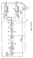
- FIG. 1 is a conceptual block diagram of a receiver that includes the automatic gain control (AGC) loop of the present invention.
- AGC automatic gain control
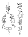
- FIG. 2 is block diagram of a first order AGC loop
- FIG. 3 is an expanded block diagram of the AGC loop, depicting the technique of the invention as it relates to adaptively changing the loop filter gain in accordance with the nature of the error signal.
- FIG. 4 is a block diagram showing how a variable AGC set-point feature may be incorporated into the AGC loop of the invention.
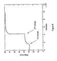
- FIG. 5 is a graph of an in-phase input signal used in simulation of AGC loop operation.
- FIG. 6 is a graph showing the in-phase signal of FIG. 5 after adjustment by the AGC loop of the invention.
- FIG. 7 is a graph showing the AGC error signal corresponding to FIGS. 5 and 6 .
- FIG. 8 is a graph showing the output of the AGC loop filter, corresponding to FIGS. 5-9 .
- the present invention pertains to automatic gain control (AGC) circuits or loops.
- AGC automatic gain control
- first-order AGC loops are preferably used in communication receivers because of their known stability of operation.
- First-order AGC loops do not, however, normally react fast enough to large signal inputs, and therefore do not provide appropriate gain control in some communication applications.
- a relatively simple, first-order AGC loop is provided with enhanced capability to adapt to large input and error signals and then to readapt to its nominal settings when the need for a more rapid response has passed.
- the invention will be described in the context of a typical communications receiver, which is conceptually illustrated in FIG. 1 .
- the receiver is shown as including a front-end analog section with amplifying, filtering and mixing stages.
- the front end of the receiver is shown as including a first low noise amplifier (LNA) indicated by reference numeral 10 and designated LNA1, which receives an incoming radio frequency (RF) signal on line 12, an image reject filter 14 coupled to the output of LNA1, and a first mixer 16 connected to receive the output of the filter and having a second input to which a local oscillator signal LO1 is applied.
- the output of the first mixer 16 is further processed by another filter 18, a second low noise amplifier 20 designated LNA2, a second mixer 22 to which a second local oscillator signal L02 is applied, another filter 24, and finally a third low noise amplifier 26 designated LNA3.
- the conceptual receiver illustrated in FIG. 1 further includes a digital module, including an analog-to-digital converter (ADC) 28, the digital output of which is connected to two parallel digital mixers 30 and 32, which have as additional inputs the in-phase and quadrature components of a digital local oscillator signal.
- ADC analog-to-digital converter
- the outputs of the digital mixers 30 and 32 are further processed by digital lowpass filters 34 and 36, respectively, which provide digital in-phase (I) and quadrature (Q) output signals on lines 38 and 40, respectively, for further processing by other components (not shown) downstream from the receiver.
- AGC loop 42 which generates appropriate amplifier control signals on lines 44, which are fed back to the low noise amplifiers 12, 20 and 26.
- the structure of the AGC loop 42 will now be discussed in more detail with reference to FIG. 2 .
- the AGC loop 42 obtains I and Q output signals from the digital low pass filters 34 and 36 on lines 38 and 40, respectively. At this point in processing, it is assumed that the I and Q digital data streams have been decimated to a data rate convenient for further processing.
- the decimated I and Q signals are separately squared in squaring circuits 50 and 52, respectively, added together in a summing circuit 54, and then further processed in a computation module 56 that generates a signal that is a measure of the input power. Further details of module 56 are discussed below.
- the measure of input power is input to a summer 58, which also receives a set-point input signal on line 60.
- the summer 58 output, on line 62, is amplified by a loop amplifier 64, which applies a loop gain of ⁇ to the difference between the set-point signal and the measure of input power. There is no amplification since ⁇ is must be less than 1.
- the loop amplifier 64 provides an output on line 66 to another summer 68, and the output of the summer 68 is connected, in turn, to a loop delay circuit 70, which interjects a delay of one sample time this process is called a running sum and serves to estimate the desired gain needed to amplify or attenuate the received signal.
- the delay circuit 70 output is fed back over line 72 to provide a second input to the summer 68.
- the output signal from the delay circuit 70 of the AGC loop is also coupled through line 74 to a gain decision and hysteresis block 76, which determines the adjustments, if any, to made to the gains of the low noise amplifiers 12, 20 and 26 ( FIG. 1 ).
- a control signal distribution 78 distributes control signals to the low noise amplifiers, as indicated by lines 44. Further details of the AGC loop are shown in FIG. 3 , in which the same reference numerals as in FIGS. 1 and 2 are used to refer to identical components.
- the computational module 56 ( FIG. 2 ) for computing a measure of input power has two subcomponents, indicated as blocks 56A and 56B.
- n refers to the sample number in a series of samples
- N denotes the total number of samples in the summation performed
- t denotes time from the start of a block of samples
- T is the time interval between samples.
- the need for performing the logarithm operation arises from the nature of a typical low-noise amplifier gain characteristic, which can be modeled as an exponential voltage gain amplifier (VGA) type of function of the form 10 (.)/10 .
- VGA exponential voltage gain amplifier
- the logarithm is also used to compress the input signal power and allow the loop to react fast to power changes.
- the output of block 56B provides a measure of the rms (root mean square) input power, designated r n , for reasons that are made more apparent from the following mathematical relationships. More precisely, the output of block 56B provides signals proportional to the square of the rms input power, i.e., r n 2 .
- the expectation operator serves as a lowpass filter to remove the effect of zero-mean white noise in the input signal.
- the envelope r n 2 has a Rayleigh distribution.
- the distribution becomes Rician in the presence of a dominant narrowband signal.
- Attack and decay time refers to the rate at which the AGC reacts to sudden increases and decreases, respectively, in the input signal. It is well known from Control theory that the attack or decay time constant is inversely proportional to the loop gain ⁇ .
- the AGC loop of the invention also includes an error signal energy detector block ( FIG. 3 ), connected between summer 58 and 68, that includes an integrate-and-dump block, connected to an output of summer 58 by line 62, that averages the error signal, a sign block connected to an output of the integrate-and-dump block, that determines the sign of the average of the error signal, and a gain and switch block, connected to a second output of the integrate-and-dump block and an input to summer 68 by line 66, to effect appropriate switching of the loop gain ⁇ .
- an error signal energy detector block FIG. 3
- the AGC is controlled to use a large loop filter gain to compensate more rapidly for the change in received signal magnitude.
- This mode is referred to as the coarse AGC mode.
- the coarse AGC loop exhibits a low loop signal-to-noise ration (SNR) to allow for fast tracking of the input signal. If the error signal energy is less than the threshold ⁇ , then the loop filter gain remains at its original low setting. This mode is known as the fine AGC mode.
- the loop exhibits a high SNR at this slower tracking speed. Therefore, the attack and decay time can change depending on the input signal condition if it is desired to change the loop behavior accordingly.
- M is a programmable parameter that indicates the number of samples taken in the averaging process.
- the sign of the average error is used to indicate whether the AGC loop is in attack mode (positive average error) or decay mode (negative average error).
- the sign determination is made in the sign block ( FIG. 3 ) and transmitted to a threshold detector and decision mechanism block, which is connected to the second output of the integrate-and-dump block and line 80.
- the decision mechanism in the threshold detector and decision mechanism block Based on the sign of the average error (which determines whether the AGC mode is attack or decay) and on the comparison of the average error with the threshold (which determines whether the AGC mode is coarse or fine), the decision mechanism in the threshold detector and decision mechanism block generates a loop gain selection signal on line 80, which results in the selection of one of four gain values by a multiplexer 82.
- the four gain values are ⁇ dc , ⁇ af , ⁇ ac and ⁇ df , where the subscripts d and a refer to the decay and attack modes, respectively, and the subscripts c and f refer to the coarse and fine modes, respectively.
- the magnitude of the average error signal is used to determine the magnitude of the loop gain, and the sign of the average error signal is used to determine whether the gain needs to be increased or decreased, based on whether the AGC is in attack or decay mode. It will be readily appreciated that the principle of the invention is not limited to use of a single threshold to determine the loop gain. One could also employ multiple thresholds and choose from a larger number of gain values.
- a further optional feature of the AGC loop of the invention is the ability to provide a variable set point P d depending on the difference between the signal energy or power, derived as previously described, and the signal energy after passing through a channel filter. If this difference is greater than a preselected threshold, a higher value of P d is chosen.
- the scheme for varying the set point is depicted in FIG. 4 .
- the digital input signals are passed through a channel filter 90, the output of which is processed in blocks 92A and 92B in much the same way that the original input signals are processed in blocks 56A and 56B.
- G is a gain adjustment and the subscript c refers to input signals passed through the channel filter.
- This estimated signal energy is input to a summer 94, the other input of which receives the estimated signal energy of the original signal, not passed through the channel filter 90.
- ⁇ is an estimate of the out-of-band noise energy before channel filtering.
- a hysteresis is often necessary when switching a gain stage on and off.
- Gain stages farthest away from the antenna are turned on first in order to minimize the noise figure of the receiver.
- the AGC loop may not switch it back off despite a drop or increase in the signal level until a certain power threshold is surpassed. Failure to present adequate hysteresis results in AM-modulating the received signal.
- the important point to note is that the fixed point implementation of the loop must be designed such that the quantized levels are much smaller than the required gain steps, which is normally the case.
- FIG. 5 is a graph showing the magnitude changes in a sample input signal, including a first step change (reduction) in magnitude and, a short time later, another step change, also reducing the magnitude.
- the second change is much greater than the first in signal power (dB) terms, specifically 10 dB for the first change versus 40 dB for the second.
- FIG. 6 plots the in-phase signal after it has been adjusted by the AGC loop of the invention. Adjustment for the second step change is achieved in approximately the same time as adjustment for the first step change, even though the second step change was a much bigger reduction in signal power. The reason for the fast reaction to the greater step change is that the second change produced an average power change that exceeded the selected threshold, and resulted in the AGC loop switching to its coarse mode of operation. This is apparent from the plot of the AGC error signal in FIG. 7 . The error signal spikes to a very large value at the time of the second step change and then quickly readjusts to a lower value. Finally, FIG. 8 shows the corresponding changes in the output of the AGC control loop.
- the present invention represents a significant advance in the field of automatic gain control technology.
- the invention provides an AGC loop that has the stability advantages of first-order control loops, but is still able to react rapidly to sudden changes in received signal power.
- AGC loop that has the stability advantages of first-order control loops, but is still able to react rapidly to sudden changes in received signal power.
- signals in the AGC loop are processed in digital form, most of the components and modules of the AGC loop are conveniently implemented in the form of software or some form of programmable hardware (firmware): The invention is not, however, limited to such implementations. Accordingly, the invention should not be limited except as by the appended claims.
Landscapes
- Control Of Amplification And Gain Control (AREA)
- Circuits Of Receivers In General (AREA)
Claims (8)
- Automatische Verstärkungsregelungs- (AGC-) Einrichtung (42) zur Erzeugung von Verstärker-Steuersignalen zur Einstellung eines sich in seiner Leistung ändernden empfangenen Kommunikationssignals auf einen gewünschten Pegel, wobei die AGC-Einrichtung (42) Folgendes umfasst:ein erstes Berechnungsmodul (56) zur Erzeugung eines Signals, das den Leistungsmittelwert des empfangenen Kommunikationssignals darstellt, wobei das erste Berechnungsmodul (56) zur Durchführung von (a) einer Integrations- und Ausgabefunktion (56A) zur Beseitigung eines Effektes eines einen Mittelwert von Null aufweisenden weißen Rauschens auf das empfangene Kommunikationssignal und nachfolgend (b) einer Logarithmus-Operation (56B) zum Komprimieren einer Signalleistung des empfangenen Kommunikationssignals angeordnet ist, um eine schnelle Reaktion auf Leistungsänderungen zu ermöglichen,ein zweites Berechnungsmodul (58) zur Erzeugung eines Fehlersignals (62), das die Differenz zwischen dem Leistungsmittelwert-Signal, das von dem ersten Berechnungsmodul (56) erzeugt wird, und einem ausgewählten Leistungs-Sollwert (60);ein drittes Berechnungsmodul zur Erzeugung eines Verstärker-Steuersignals aus dem Fehlersignal, wobei das erzeugte Verstärker-Steuersignal auf Änderungen des Leistungsmittelwertes des empfangenen Signals anspricht, wobei das dritte Berechnungsmodul einen Schleifenverstärker (54) zur Verstärkung des Fehlersignals, ein Summiermodul (68) zum Kombinieren des verstärkten Fehlersignals mit einem anderen Eingangssignal, und ein Verzögerungsmodul (70) zum Empfang des Summiermoduls (68) und zur Lieferung des Verstärker-Steuersignals als Ausgangssignal umfasst, wobei das andere Eingangssignal (72) des Summiermoduls (68) von dem Verstärker-Steuersignal in einem früheren Berechnungszyklus abgeleitet ist; undein viertes Berechnungsmodul zur Steuerung der Verstärkung des Schleifenverstärkers (64) entsprechend der mittleren Fehlersignal-Leistung (62), wobei das vierte Berechnungsmodul ein Fehlersignal-Leistungs-Bestimmungsmodul, ein Fehlersignal-Vorzeichen-Bestimmungsmodul und ein Verstärkungs-Entscheidungsmodul umfasst, das Eingangssignale von dem Fehlersignal-Leistungs-Bestimmungsmodul und dem Fehlersignal-Vorzeichen-Bestimmungsmodul empfängt und eine Schleifenverstärker-Verstärkung (µ) auf der Grundlage der empfangenen Eingangssignale auswählt (80),wobei das Verstärkungs-Entscheidungsmodul ein Vergleichermodul zum Vergleichen der empfangenen mittleren Fehlersignal-Leistung (62) mit einem Schwellenwert und ein Vorzeichen-Detektionsmodul zur Feststellung des algebraischen Vorzeichens der mittleren Fehlersignal-Leistung umfasst,wobei das Verstärkungs-Entscheidungsmodul zur Auswahl von einer von vier Schleifenverstärker-Werten aus einem Paar von Feinbetriebsart-Verstärkungswerten (µaf, µdf) und eines Paares von Grobbetriebsart-Verstärkungswerten (µac, µdc), wobei jedes Paar einen Verstärkungswert für eine Anstiegs-Betriebsart und einen Verstärkungswert für eine Abfall-Betriebsart enthält, durch Auswahl eines Paares von Feinbetriebsart-Schleifenverstärker-Verstärkungswerten (µaf, µdf) wenn die empfangene mittlere Fehlersignal-Leistung (62) unterhalb des Schwellenwertes liegt, oder zur Auswahl eines Paares von Grobbetriebsart-Schleifenverstärker-Verstärkungswerten (µac, µdc) angeordnet ist, wenn die empfangene mittlere Fehlersignal-Leistung (62) oberhalb des Schwellenwertes liegt, und wobei ein Vorzeichen-basiertes Auswahlmodul so angeordnet ist, dass es einen Anstiegs-Betriebsart- oder einen Abfall-Betriebsart-Verstärkungswert aus dem ausgewählten Paar von Grob- oder Feinbetriebsart-Verstärkungswerten auf der Grundlage des Vorzeichens der empfangenen mittleren Fehlersignal-Leistung (62) auswählt.
- AGC-Einrichtung (42) nach Anspruch 1, bei der das erste Berechnungsmodul (56) zur Erzeugung eines Signals proportional zu dem Quadrat der Effektivwert- (rms-) Leistung des empfangenen Kommunikationssignals angeordnet ist.
- AGC-Einrichtung (42) nach Anspruch 1, die weiterhin ein Sollwert-Auswahlmodul (96) umfasst, wobei der Leistungs-Sollwert, der dem zweiten Berechnungsmodul (58) zugeführt wird, so angeordnet ist, dass er automatisch auf der Grundlage von Messungen ausgewählt wird, die an dem empfangenen Kommunikationssignal durchgeführt werden.
- AGC-Einrichtung (42) nach Anspruch 3, die weiterhin Folgendes umfasst:ein Kommunikationskanal-Modell (90), dem das empfangene Kommunikationssignal als Eingang zugeführt wird,ein Integrations- und Ausgabe- und Logarithmus-Operationsmodul, das im Wesentlichen ähnlich zu dem ersten Berechnungsmodul (56) ist, jedoch so angeordnet ist, dass es ein Signal erzeugt, das den Leistungsmittelwert des empfangenen Kommunikationssignals nach dem Durchlaufen des Kanal-Modells darstellt; undein Differenzmodul (94), das zur Erzeugung eines Differenzsignals angeordnet ist, das die Differenz zwischen dem Leistungsmittelwert des empfangenen Signals und dem Leistungsmittelwert des empfangenen Signals nach dem Durchlaufen des Kanal-Modells darstellt,wobei das Sollwert-Auswahlmodul (96) so angeordnet ist, dass es einen Sollwert auf der Grundlage des Wertes des Differenzsignals im Vergleich zu einem Schwellenwert ausführt.
- Verfahren zur automatischen Verstärkungsregelung zur Verwendung in einem Kommunikationsempfänger, mit den folgenden Schritten:Erzeugen einer Signal-Darstellung des Leistungsmittelwertes eines empfangenen Kommunikationssignals über (a) eine Integrations- und Ausgabefunktion (56A) zur Beseitigung eines Effektes eines einen Mittelwert von Null aufweisenden weißen Rauschens auf das empfangene Kommunikationssignal und nachfolgend (b) einer Logarithmus-Operation (56B) an einem Ausgang der Integrations- und Ausgabefunktion zum Komprimieren einer Signalleistung des empfangenen Kommunikationssignals, um eine schnelle Reaktion auf Leistungsänderungen zu ermöglichen,Erzeugen einer mittleren Fehlersignal-Leistung (62), die die Unterschiede zwischen dem Leistungsmittelwert-Signal und einem ausgewählten Leistungs-Sollwert darstellt,Erzeugen eines Verstärker-Steuersignals aus der mittleren Fehlersignal-Leistung (62), wobei das erzeugte Verstärker-Steuersignal auf Änderungen in der mittleren Leistung des empfangenen Signals anspricht, durch Verstärken des Fehlersignals (82) in einem Schleifenverstärker (64), Kombinieren des verstärkten Fehlersignals (66) mit einem weiteren Eingangssignal (72) zur Erzeugung eines Summensignals, Verzögern des Summensignals und Liefern eines Verstärker-Steuersignals als Ausgangssignal, und Zuführen des verzögerten Ausgangssignals zurück zur Verwendung als das andere Eingangssignal (72) in dem Kombinationsschritt, wobei das andere Eingangssignal (72) von dem Verstärker-Steuersignal in einem früheren Berechnungszyklus abgeleitet wurde, undSteuern der Verstärkung des Schleifenverstärkers (64) entsprechend der mittleren Fehlersignal-Leistung (62) unter Einschluss der Bestimmung der mittleren Leistung des Fehlersignals, der Bestimmung des algebraischen Vorzeichens der mittleren Leistung des Fehlersignals und des Vergleichs der mittleren Fehlersignal-Leistung (62) mit einem Schwellenwert, undAuswahl eines von vier Schleifenverstärker-Verstärkungswerten aus einem Paar von Feinbetriebsart-Verstärkungswerten (µaf, µdf) und eines Paares von Grobbetriebsart-Verstärkungswerten (µac, µdc), wobei jedes Paar einen Verstärkungswert für die Anstiegs-Betriebsart und einen Verstärkungswert für die Abfall-Betriebsart enthält, durch Auswählen eines Paares von Feinbetriebsart-Schleifenverstärker-Verstärkungswerten (µaf, µdf), wenn die empfangene mittlere Fehlersignal-Leistung (62) unterhalb des Schwellenwertes liegt, oder Auswählen eines Paares von Grobbetriebsart-Schleifenverstärker-Verstärkungswerten (µac, µdc), wenn die empfangene mittlere Fehlersignal-Leistung (62) oberhalb des Schwellenwertes liegt, und Auswählen eines Anstiegs-Betriebsart- oder eines Abfall-Betriebsart-Verstärkungswertes aus dem ausgewählten Paar von Grob- und Feinbetriebsart-Verstärkungswerten auf der Grundlage des Vorzeichens der empfangenen mittleren Fehlersignal-Leistung.
- Verfahren nach Anspruch 5, bei dem der Schritt des Erzeugens eines den Leistungsmittelwert des Kommunikationssignals darstellenden Signals die Erzeugung eines Signals proportional zum Quadrat der Effektivwert- (rms-) Leistung des empfangenen Kommunikationssignals umfasst.
- Verfahren nach Anspruch 5, das weiterhin die automatische Auswahl des Leistungs-Sollwertes umfasst, der in dem Schritt der Erzeugung eines Fehlersignals auf der Grundlage von Messungen verwendet wird, die an dem empfangenen Kommunikationssignal durchgeführt werden.
- Verfahren nach Anspruch 7, bei dem der Schritt des automatischen Auswählens des Leistungs-Sollwertes Folgendes umfasst:Eingabe des empfangenen Kommunikationssignals in ein Kommunikationskanal-Modell (90);Erzeugen eines den Leistungsmittelwert des empfangenen Kommunikationssignals nach dem Durchlaufen des Kanalmodells darstellenden Signals;Erzeugen eines Differenzsignals, das die Differenz zwischen dem Leistungsmittelwert des empfangenen Signals und dem Leistungsmittelwert des empfangenen Signals nach dessen Durchlaufen durch das Kanalmodell darstellt; undAuswählen eines Leistungs-Sollwertes auf der Grundlage des Wertes des Differenzsignals im Vergleich mit einem Schwellenwert.
Priority Applications (1)
| Application Number | Priority Date | Filing Date | Title |
|---|---|---|---|
| EP10182387A EP2259424B1 (de) | 2004-11-02 | 2005-11-02 | Automatische Verstärkungsregelung mit Regelschleifeverstärkungssteuerung |
Applications Claiming Priority (1)
| Application Number | Priority Date | Filing Date | Title |
|---|---|---|---|
| US10/979,703 US7366490B2 (en) | 2004-11-02 | 2004-11-02 | Automatic gain control with gain stepping and regulation |
Related Child Applications (1)
| Application Number | Title | Priority Date | Filing Date |
|---|---|---|---|
| EP10182387.0 Division-Into | 2010-09-29 |
Publications (2)
| Publication Number | Publication Date |
|---|---|
| EP1653610A1 EP1653610A1 (de) | 2006-05-03 |
| EP1653610B1 true EP1653610B1 (de) | 2013-01-02 |
Family
ID=35687408
Family Applications (2)
| Application Number | Title | Priority Date | Filing Date |
|---|---|---|---|
| EP10182387A Ceased EP2259424B1 (de) | 2004-11-02 | 2005-11-02 | Automatische Verstärkungsregelung mit Regelschleifeverstärkungssteuerung |
| EP05256790A Ceased EP1653610B1 (de) | 2004-11-02 | 2005-11-02 | Automatische Verstärkungsregelung mit Regelschleifeverstärkungssteuerung |
Family Applications Before (1)
| Application Number | Title | Priority Date | Filing Date |
|---|---|---|---|
| EP10182387A Ceased EP2259424B1 (de) | 2004-11-02 | 2005-11-02 | Automatische Verstärkungsregelung mit Regelschleifeverstärkungssteuerung |
Country Status (2)
| Country | Link |
|---|---|
| US (1) | US7366490B2 (de) |
| EP (2) | EP2259424B1 (de) |
Families Citing this family (12)
| Publication number | Priority date | Publication date | Assignee | Title |
|---|---|---|---|---|
| US7248847B2 (en) * | 2004-04-22 | 2007-07-24 | Kyocera Wireless Corp. | System and method for adaptively controlling receiver gain switch points |
| US7187915B2 (en) * | 2004-09-28 | 2007-03-06 | Via Technologies, Inc. | Automatic gain control for a WLAN system |
| US7830991B2 (en) * | 2005-10-03 | 2010-11-09 | Harris Corporation | Frequency selective automatic gain control with dual non-symmetric attack and release times and interference detection feature |
| US8189724B1 (en) | 2005-10-26 | 2012-05-29 | Zenith Electronics Llc | Closed loop power normalized timing recovery for 8 VSB modulated signals |
| KR100799919B1 (ko) * | 2005-12-30 | 2008-02-01 | 포스데이타 주식회사 | 무선통신 시스템의 자동이득제어 장치 및 방법 |
| TWI389467B (zh) * | 2009-04-08 | 2013-03-11 | Ind Tech Res Inst | 自動增益控制方法及裝置 |
| CN101882918B (zh) * | 2009-05-07 | 2014-01-08 | 财团法人工业技术研究院 | 自动增益控制方法及装置 |
| US8634766B2 (en) | 2010-02-16 | 2014-01-21 | Andrew Llc | Gain measurement and monitoring for wireless communication systems |
| EP2608404B1 (de) * | 2011-12-20 | 2016-07-27 | Telefonaktiebolaget LM Ericsson (publ) | Verfahren und Vorrichtung zur Durchführung einer automatischen Verstärkungsregelung eines empfangenen Signals |
| CN102571013A (zh) * | 2012-01-17 | 2012-07-11 | 钜泉光电科技(上海)股份有限公司 | 用于通信接收机中的自动增益控制装置及其方法 |
| US8660221B2 (en) * | 2012-06-14 | 2014-02-25 | Issc Technologies Corp. | Fast and robust AGC apparatus and method using the same |
| EP3116127B1 (de) | 2015-07-08 | 2018-09-12 | Power Integrations Switzerland GmbH | Empfängerschaltung |
Family Cites Families (11)
| Publication number | Priority date | Publication date | Assignee | Title |
|---|---|---|---|---|
| JPH06244889A (ja) * | 1993-02-15 | 1994-09-02 | Fujitsu Ltd | モデム復調部用受信レベル調整回路 |
| US5563916A (en) * | 1995-06-05 | 1996-10-08 | Hitachi America, Ltd. | Apparatus and method for varying the slew rate of a digital automatic gain control circuit |
| US5627857A (en) * | 1995-09-15 | 1997-05-06 | Qualcomm Incorporated | Linearized digital automatic gain control |
| US6154503A (en) * | 1996-06-07 | 2000-11-28 | Sharp Kk Corporation | Automatic gain control system that responds to baseband signal distortion |
| US6212244B1 (en) * | 1998-01-09 | 2001-04-03 | Golden Bridge Technology, Inc. | Fast response automatic gain control |
| US6081565A (en) * | 1998-02-05 | 2000-06-27 | Lucent Technologies Inc. | Amplitude based coarse automatic gain control circuit |
| JP3739985B2 (ja) * | 2000-01-31 | 2006-01-25 | 富士通株式会社 | 送信機利得安定化装置 |
| MY130364A (en) * | 2000-05-15 | 2007-06-29 | Matsushita Electric Industrial Co Ltd | Digital demodulation apparatus |
| KR100452308B1 (ko) | 2000-06-13 | 2004-10-12 | 마쯔시다덴기산교 가부시키가이샤 | 디지털 방송수신장치 |
| US6968166B2 (en) * | 2002-01-22 | 2005-11-22 | George L. Yang | Method and apparatus of a fast digital automatic gain control circuit |
| JP3715606B2 (ja) * | 2002-09-10 | 2005-11-09 | 株式会社東芝 | 無線通信機及びその制御方法 |
-
2004
- 2004-11-02 US US10/979,703 patent/US7366490B2/en not_active Expired - Lifetime
-
2005
- 2005-11-02 EP EP10182387A patent/EP2259424B1/de not_active Ceased
- 2005-11-02 EP EP05256790A patent/EP1653610B1/de not_active Ceased
Also Published As
| Publication number | Publication date |
|---|---|
| US7366490B2 (en) | 2008-04-29 |
| EP2259424A1 (de) | 2010-12-08 |
| US20060094384A1 (en) | 2006-05-04 |
| EP1653610A1 (de) | 2006-05-03 |
| EP2259424B1 (de) | 2012-07-04 |
Similar Documents
| Publication | Publication Date | Title |
|---|---|---|
| US8553815B2 (en) | Gain control for a receiver in a multi-carrier communication system | |
| CN102656806B (zh) | 管理接收机的正交信号路径中的自动增益控制的电路、系统和方法 | |
| EP1653610B1 (de) | Automatische Verstärkungsregelung mit Regelschleifeverstärkungssteuerung | |
| EP1230738B1 (de) | Radioempfänger mit komplexen filtern und komplexer verstärkungsregelung für niedrige oder null hertz zwischenfrequenz | |
| US6826418B2 (en) | Radio circuit and control method of radio circuit | |
| US20070086547A1 (en) | AGC for narrowband receivers | |
| EP1634380A1 (de) | Adaptiver intermodulationsverzerrungsfilter für direktkonversionsempfänger | |
| US8804882B2 (en) | Receiving apparatus, and computer readable memory medium that stores a program | |
| EP2817881B1 (de) | Qualitätsindikator für empfangene signale | |
| EP2688214A1 (de) | Verstärkungsregelungsschaltung, kommunikationsvorrichtung, elektronische vorrichtung und verstärkungsregelungsverfahren | |
| US8055232B2 (en) | Radio frequency receiving apparatus, radio frequency receiving method, LSI for radio frequency signal and LSI for base band signal | |
| EP2458733B1 (de) | Automatische Vorwärtsverstärkungskorrektur | |
| US20040171365A1 (en) | Off-channel signal detector with programmable hysteresis | |
| JP4574687B2 (ja) | Rf受信装置 | |
| US6628932B1 (en) | Radio receiver automatic gain control techniques | |
| EP1499014B1 (de) | Verfahren zur automatischen Verstärkungsregelung, beispielsweise in einem Telekommunikationssystem, Vorrichtung und Computerprogramm hierfür | |
| US4185243A (en) | Method and apparatus for providing a standby signal | |
| JP4148813B2 (ja) | 受信回路およびこれを用いた移動無線受信機 | |
| JPH1013282A (ja) | 無線受信器の電力節約の方法 | |
| JP2005192060A (ja) | 自動利得制御装置 | |
| WO2006020950A1 (en) | Automatic gain control unit of a receiver | |
| US8190028B2 (en) | Method and apparatus for treating a received signal to present a resulting signal with improved signal accuracy | |
| JP2861877B2 (ja) | 受信装置 | |
| JPH05335981A (ja) | 受信機 |
Legal Events
| Date | Code | Title | Description |
|---|---|---|---|
| PUAI | Public reference made under article 153(3) epc to a published international application that has entered the european phase |
Free format text: ORIGINAL CODE: 0009012 |
|
| AK | Designated contracting states |
Kind code of ref document: A1 Designated state(s): AT BE BG CH CY CZ DE DK EE ES FI FR GB GR HU IE IS IT LI LT LU LV MC NL PL PT RO SE SI SK TR |
|
| AX | Request for extension of the european patent |
Extension state: AL BA HR MK YU |
|
| 17P | Request for examination filed |
Effective date: 20060703 |
|
| 17Q | First examination report despatched |
Effective date: 20060802 |
|
| AKX | Designation fees paid |
Designated state(s): DE |
|
| 17Q | First examination report despatched |
Effective date: 20060802 |
|
| RAP1 | Party data changed (applicant data changed or rights of an application transferred) |
Owner name: NORTHROP GRUMMAN SYSTEMS CORPORATION |
|
| GRAP | Despatch of communication of intention to grant a patent |
Free format text: ORIGINAL CODE: EPIDOSNIGR1 |
|
| GRAS | Grant fee paid |
Free format text: ORIGINAL CODE: EPIDOSNIGR3 |
|
| GRAA | (expected) grant |
Free format text: ORIGINAL CODE: 0009210 |
|
| AK | Designated contracting states |
Kind code of ref document: B1 Designated state(s): DE |
|
| REG | Reference to a national code |
Ref country code: DE Ref legal event code: R096 Ref document number: 602005037688 Country of ref document: DE Effective date: 20130307 |
|
| PLBE | No opposition filed within time limit |
Free format text: ORIGINAL CODE: 0009261 |
|
| STAA | Information on the status of an ep patent application or granted ep patent |
Free format text: STATUS: NO OPPOSITION FILED WITHIN TIME LIMIT |
|
| 26N | No opposition filed |
Effective date: 20131003 |
|
| REG | Reference to a national code |
Ref country code: DE Ref legal event code: R097 Ref document number: 602005037688 Country of ref document: DE Effective date: 20131003 |
|
| PGFP | Annual fee paid to national office [announced via postgrant information from national office to epo] |
Ref country code: DE Payment date: 20201119 Year of fee payment: 16 |
|
| REG | Reference to a national code |
Ref country code: DE Ref legal event code: R119 Ref document number: 602005037688 Country of ref document: DE |
|
| PG25 | Lapsed in a contracting state [announced via postgrant information from national office to epo] |
Ref country code: DE Free format text: LAPSE BECAUSE OF NON-PAYMENT OF DUE FEES Effective date: 20220601 |