EP1655827B1 - Dispositif et procédé de commande d'un convertisseur d'énergie électrique et convertisseur comportant un tel dispositif - Google Patents
Dispositif et procédé de commande d'un convertisseur d'énergie électrique et convertisseur comportant un tel dispositif Download PDFInfo
- Publication number
- EP1655827B1 EP1655827B1 EP05354033A EP05354033A EP1655827B1 EP 1655827 B1 EP1655827 B1 EP 1655827B1 EP 05354033 A EP05354033 A EP 05354033A EP 05354033 A EP05354033 A EP 05354033A EP 1655827 B1 EP1655827 B1 EP 1655827B1
- Authority
- EP
- European Patent Office
- Prior art keywords
- arms
- voltage
- signals
- modulation
- control
- Prior art date
- Legal status (The legal status is an assumption and is not a legal conclusion. Google has not performed a legal analysis and makes no representation as to the accuracy of the status listed.)
- Expired - Lifetime
Links
Images





Classifications
-
- H—ELECTRICITY
- H02—GENERATION; CONVERSION OR DISTRIBUTION OF ELECTRIC POWER
- H02M—APPARATUS FOR CONVERSION BETWEEN AC AND AC, BETWEEN AC AND DC, OR BETWEEN DC AND DC, AND FOR USE WITH MAINS OR SIMILAR POWER SUPPLY SYSTEMS; CONVERSION OF DC OR AC INPUT POWER INTO SURGE OUTPUT POWER; CONTROL OR REGULATION THEREOF
- H02M5/00—Conversion of AC power input into AC power output, e.g. for change of voltage, for change of frequency, for change of number of phases
- H02M5/40—Conversion of AC power input into AC power output, e.g. for change of voltage, for change of frequency, for change of number of phases with intermediate conversion into DC
- H02M5/42—Conversion of AC power input into AC power output, e.g. for change of voltage, for change of frequency, for change of number of phases with intermediate conversion into DC by static converters
- H02M5/44—Conversion of AC power input into AC power output, e.g. for change of voltage, for change of frequency, for change of number of phases with intermediate conversion into DC by static converters using discharge tubes or semiconductor devices to convert the intermediate DC into AC
- H02M5/453—Conversion of AC power input into AC power output, e.g. for change of voltage, for change of frequency, for change of number of phases with intermediate conversion into DC by static converters using discharge tubes or semiconductor devices to convert the intermediate DC into AC using devices of a triode or transistor type requiring continuous application of a control signal
- H02M5/458—Conversion of AC power input into AC power output, e.g. for change of voltage, for change of frequency, for change of number of phases with intermediate conversion into DC by static converters using discharge tubes or semiconductor devices to convert the intermediate DC into AC using devices of a triode or transistor type requiring continuous application of a control signal using semiconductor devices only
- H02M5/4585—Conversion of AC power input into AC power output, e.g. for change of voltage, for change of frequency, for change of number of phases with intermediate conversion into DC by static converters using discharge tubes or semiconductor devices to convert the intermediate DC into AC using devices of a triode or transistor type requiring continuous application of a control signal using semiconductor devices only having a rectifier with controlled elements
Definitions
- the invention also relates to such a converter comprising said control device and a method for controlling such a converter.
- Such a converter 1 represented on the figure 1 usually has lines L1 and L2 of DC voltage VDC and an inverter 2 formed by power semiconductor arms 2A, 2B, 2C connected between the lines L1 and L2 for outputting alternating voltages VO to a load 3 or to an electrical distribution network.
- the electric filters 4 may be interposed between the outputs of the arms 2A, 2B, 2C and the load 3 or the network.
- a rectifier 5 connected between AC VI inputs and lines L1 and L2 provides DC voltage VDC.
- Capacitors C1 and C2 connected to the lines L1 and L2 filter the DC voltage VDC.
- the load When the load is unbalanced, it is necessary to distribute a neutral conductor output to ensure correct voltages.
- the load comprises a neutral conductor LN connected to a midpoint of the capacitors C1 and C2 filtering. Generally its capacitors have very high values to ensure a good stability of the voltage even with very strong neutral currents.
- a control device 6 controls the semiconductors of the arms to provide alternating voltages referenced in particular with respect to the neutral conductor.
- the neutral line LN can be connected to a fourth arm 2N of the inverter 2 .
- the arm 2N is connected like the other arms between the lines L1 and L2 of DC voltage.
- the figure 4 shows an example of a part of a processing unit 7 of a control circuit 6 for providing control signals of the arms.
- a regulator 8 makes it possible to regulate and supply three-phase modulation signals as a function of reduced setpoints Cd, Cq, Co, in particular by a Park or Concordia transformation in the dqo or ⁇ o domains. These known transformations and rotations are generally calculated using so-called Park and Concordia matrices respectively.
- MC1 signals for each output phase of the controller are preferably used for intersective type modulation on a high frequency carrier triangular signal for pulse width modulation.
- the regulator 8 supplies first three-phase modulation signals MC1, a module 9 determines overmodulation signals OM to be applied to the first signals MC1 with operators 10, a module 11 applies a reference voltage V2 to MC1 signals by operators 12, and a module 13 provides a high frequency signal intended to be modulated by MC2 modulation signals modified by the operators 10 and 12.
- the operators 14 combine the MC2 modulation signals with high frequency signals F1 preferably triangular to provide control signals CVA, CVB and CVC of the inverter arms 2A, 2B, 2C in pulse width modulation format. Since the controls of the arms are preferably binary in saturated-blocked mode, a conditioning circuit 16 formats the control signals.
- the overmodulation signals OM are generated by the modulation signals MC1 and by the type of overmodulation.
- the reference signal V2 is generally representative of a DC voltage, for example half of the voltage VDC of lines L1 and L2.
- the figure 5 represents a known converter with common neutral or through neutral.
- This converter used as an uninterruptible power supply comprises a battery 17 connected through an adapter 18 to the lines L1 and L2 of DC voltage.
- this converter comprises a rectifier 19 with three arms 19A, 19B and 19C connected to inputs 20 of voltages or alternating currents and lines L1 and L2 of DC voltage VDC.
- a control circuit 21 of the rectifier controls the arms of the rectifier as a function of the DC voltage VDC and of the currents to be taken on a network connected at the input 20.
- the filtering capacitors have a common point connected to the line LN of the traversing neutral.
- the voltage of the common point of the capacitors is generally a median voltage between lines L1 and L2 whose value is set by semiconductors T1 and T2 of voltage regulation controlled by a control circuit 22.
- an inverter of the same type as that of the figure 2 is connected on lines L1 and L2 and on the middle point of the capacitors.
- capacitors do not need to be very high values.
- the value of the capacitors is high to absorb the currents of neutral without too much disturb the DC voltage VDC.
- the value and size of the filter capacitors C1 and C2 can become very high.
- the high values of the capacitors are due in particular to the filtering and absorption of the neutral currents of the load supplied by the inverter as well as the neutral currents of the source which supplies the rectifier.
- High capacitance capacitance values in this case ensure independence between the structures of the inverter and those of the rectifier. Thus, strong currents neutral on the side inverters have little disruptive effects on the rectifier or the currents of the source.
- the known devices of the state of the art with neutral through such as that of the figure 5 have very high capacitance capacitance values which involve very considerable costs when the power of the converter is high.
- the coupling of the neutral currents does not make it possible to reduce the power in the semiconductors by over-modulation on the controls of the arms of the inverter and the rectifier when the currents are unbalanced.
- the lack of over-modulation in the controls causes a loss of power when switching semiconductors and imposes a higher DC voltage and lower converter electrical efficiency.
- the introduction of additional neutral arms for the inverter and the four-arm rectifier is not possible with a neutral through because the known control devices do not allow to control the neutral currents of the inverter and the rectifier. sufficiently independently to limit the coupling between the rectifier, the inverter and the DC voltage lines.
- the invention relates to a converter comprising a control device according to claim 1 and a control method according to claim 13.
- the object of the invention is to provide a device and a method for controlling an electric energy converter and a converter comprising such a device making it possible to solve the problems of forward-to-neutral converters of the state of the art.
- control means control a common arm comprising electronic power components connected between said intermediate DC voltage lines and the common link, said processing means controlling said common arm as a function of a modulation signal of said determined common arm with a reference voltage setpoint having a value representative of a voltage between said intermediate lines .
- the representative voltage reference signals are the same for the determination of the modulation signals of each modulated arm of the converter and the carrier signals are the same for the determination of the control signals of each arm of the converter.
- the processing means comprise means for determining a general control component for the processing of an over-modulation, said general control component being determined as a function of the first modulation signals of the arms of the conversion means, and a signal Representative of the general control component is used to process modulation signals of the conversion means arms and a modulation signal of the common arm.
- the processing means use a signal representative of the general control component to process modulating signals of the arms of the recovery means.
- the processing means comprise correction means for correcting said general control component as a function of signals representative of saturation of first modulation signals of the recovery means.
- the correction means comprise means for predicting saturation values and means for reducing a signal representative of the general control component as a function of said saturation values.
- said processing means provide modulation signals of the arms of conversion means representative of voltages different from the corresponding voltages of the input voltages of the rectifying means.
- said processing means provide modulation signals of the arms of the conversion means having a fundamental frequency of frequency different from the fundamental frequency of the input voltage of the rectifying means.
- said processing means provide modulation signals of the arms of the conversion means having phases different from the phases of the input voltage of the rectifying means.
- said control means of the control device control the conduction of the arms of said converting means and the rectifying means arms reversibly, outputs to a load becoming energy inputs, the conversion means becoming means of straightening, and the inputs becoming outputs to provide AC power.
- the method comprises a second step of determining a general control component value, and a second application step for applying said general control component to said modulation signals.
- the method comprises a third application step for applying to modulating signals for the arm control of the rectifying means a reference voltage setpoint and the general control component value.
- the method comprises a step of detecting the saturation of the arm control modulation signals of the rectifying means, and a step of correcting the general control component value as a function of the saturation detection of the arm modulation signals. rectification means.
- the converter comprises a common arm 32 comprising electronic components 32A and 32B of power connected between said intermediate lines L1 and L2 of DC voltage VDC and the common connection LN of neutral.
- the additional common arm 32 controls the neutral currents by allowing an additional level of control to decrease the size of the capacitors.
- the neutral currents passing through this additional arm also make it possible to introduce a controlled over-modulation and to reduce the voltage of the DC voltage line to reduce switching losses.
- the control device 31 controls said common arm 32 as a function of a modulation signal MCom of said determined common arm with a reference voltage setpoint V2.
- the modulation signal MCom of the common arm modulates a carrier signal F1 which is preferably close to or similar to a carrier signal F1 used for the control of the arms of the inverter and the arms of the rectifier.
- the reference voltage setpoint V2 for modulation signals of the common arm is preferably close to or similar to reference voltage setpoints V2 for modulation signals of the arms of the inverter 2 and the arms of the inverter 19.
- the control of the common arm, the control of the arms of the inverter and the control of the arms of the rectifier have the same bases of carrier signal F1 and reference voltage setpoint V2.
- the modulation signals representative of the input voltage of the rectifier and of the output of the inverter can be independent since the neutral currents that can circulate in the common arm are synchronized by the carrier signal F1.
- the characteristics of the voltages and currents of the input network may be different from the characteristics of the output voltages of the inverter.
- the output voltage VO of the inverter may have a voltage value different from the voltage VI of the input network, but also a different phase or a different frequency.
- this through-neutral converter can also operate reversibly.
- the control device controls the conduction of the arms of the inverter and the arms of the rectifier in a reversible manner. Outputs to a load then become energy inputs, the inverter becomes a rectifier, and the inputs become outputs to provide AC power.
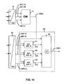
- the figure 7 represents a block diagram of a processing unit 7 of a control circuit 31 of a control device according to one embodiment of the invention.
- the control device is intended in particular to control the conduction of semiconductor arms of an electric energy converter according to the figure 6 .
- the control circuit controls the conduction of the arms 2A, 2B, 2C of the inverter and includes a processing unit 7 for supplying modulation signals MC2A, MC2B and MC2C of control signals CVA, CVB, CVC of said arms.
- the control circuit controls a common arm 32 comprising power electronic components 32A and 32B connected in series between said intermediate lines L1 and L2 of DC voltage VDC and connected to the common neutral connection. LN by their common midpoint.
- the processing unit modulates said common arm as a function of a determined modulation signal Mcom with a reference voltage setpoint V2.
- the modulation signal Mcom of the common arm is combined in an operator 33 to modulate a carrier signal of F1.
- a regulator 8 supplies first three-phase MC1A, MC1B and MC1C signals for modulation of the inverter 2
- a second regulator 34 supplies first three-phase MR1A, MR1B, MR1C signals for the modulation of the rectifier 19.
- the first modulation signals of the inverter are combined in operators 12 with a reference voltage setpoint V2 to provide second modulated inverter modulation signals respectively MC2A, MC2B, MC2C.
- the first rectifier modulation signals are combined in operators with a reference voltage setpoint V2 to provide second modified modulation signals MR2A, MR2B, MR2C respectively of the rectifier.
- Modulated modulation signals MR1A, MR1B, MR1C and MC2A, MC2B, MC2C are combined in operators respectively 14 and 36 for modulating carrier signals F1.
- the setpoint V2 applied to the operators 12, 35, 33 is of the same nature and the carrier F1 applied to the operators 14, 36 and 33 is of the same nature.
- the same voltage V2 is applied to the operators 12, 35 and 33, and / or the same carrier signal F1 is applied to the operators 14, 36 and 33.
- Modulated CVA, CVB, CVC signals are intended for the control of the arms of the inverter
- modulated CRB, CRB, CRC signals are intended for the control of the arms of the rectifier
- a Ccom signal is intended for the control of the common arm.
- the modulation of the signals is preferably modulated pulse width modulation for example in the operators 14, 36 and 33 according to a so-called intersective method.
- the figure 8 represents a block diagram of a control circuit 31 of a control device with an overmodulation function.
- a module 9 receives the first modulation signals of the inverter MC1A, MC1B, MC1C supplied by the regulator and determines a general OM control component comprising overmodulation and control signals of the common arm 32.
- This OM component is combined with the first modulation signals of the inverter MC1A, MC1B, MC1C in operators 10 and combined with the reference voltage reference signal V2 in an operator 37 to provide a modulation signal MCom of the common arm.
- the control device of the figure 9 comprises a saturation detection module 38.
- the module 38 receives the first signals MR1A, MR1B, MR1C for modulating the arms of the rectifier and a first signal OMO of general control component.
- the module 38 detects the risk of saturation and corrects the general control component signal OM0 as a function of exceeding a saturation limit value.
- a new corrected general component signal OM1 is combined with the first modulation signals of the arms of the inverter in operators 10, with the first MR1A, MR1B, MR1C for modulating the arms of the rectifier in operators 39, and with the reference voltage signal V2 in an operator 37 for the control of the common arm.
- the modulation signals of the arms of the inverter are also combined in operators 12 with the signal V2 of reference voltage and in operators 14 with a carrier signal F1
- the modulation signals of the arms of the rectifier are also combined in operators with the reference voltage signal V2 and in operators 36 with a carrier signal F1.
- the operator 37 provides a common arm modulation signal Mcom resulting from the corrected general control component OM1 and the reference voltage signal V2.
- the Mcom signal is combined with the carrier signal in the F1 operator.
- the figure 10 represents an exemplary block diagram of a module 38 for correcting a general control component.
- Said general control component is corrected according to signals representative of saturation of the modulation signals of the rectifying means.
- the module 38 comprises saturation value determination modules 41, 42, 43 respectively SA, SB, SC for each modulation signal of the arms of the rectifier.
- the modules 41, 42, 43 receive as input the first signals respectively MR1A, MR1B, MR1C for modulating the rectifier and the first signal of the general control component OM0 and output saturation value signals SA, SB, SC respectively. . If a saturation risk is detected, the first control component signal and the saturation overflow value signals SA, SB, SC are combined in an operator 44 to correct the first control component signal and to provide a control signal.
- the modules 41, 42, and 43 determine or predict saturation values SA, SB, SC and the operator 44 reduces a signal representative of the general control component OM1 as a function of said saturation values.
- the general control component, the carrier signal and / or the reference voltage signal are common to the entire processing of the arms of the inverter, the rectifier and of the common arm.
- the processing unit may provide modulation signals of the inverter arms having voltages different from the corresponding voltages of the rectifier input voltages and / or modulation signals of the inverter arms having a fundamental frequency of frequency different from the fundamental frequency of the rectifier input voltage and / or the modulation signals of the inverter arms having phases different from the phases of the rectifier input voltage.
- the figure 11 represents an exemplary flowchart of a control method of an electric energy converter according to the invention.
- the method comprises a first step 60 for determining modulation signals MC1A, MC1B, MC1C for the arm control of the inverter.
- a second determination step 61 determines a general control component value OM0 as a function of the first modulation signals of the inverter and possibly of the type of overmodulation chosen.
- a value representative of said general control component is applied to the modulation signals of the inverter and the common arm.
- a step 63 makes it possible to apply to the modulation signals of the arms of the inverter MC1A, MC1B, MC1C and to a modulation signal Mcom of the common arm a reference voltage setpoint V2.
- a third determining step 64 determines modulation signals for the rectifier arm control as a function of a reference voltage setpoint V2 and a general control component value OM.
- a phase 65 of saturation management comprises steps of correction of the general control component in case of saturation risks of the control of the arms of the rectifier.
- a detection step 66 detects a risk of saturation of the rectifier arm control modulation signals
- a step 67 determines a saturation overshoot value Vsat by evaluating said exceeding of a first value of the general component of the rectifier. OMO command with a saturation limit value Vmax.
- a correction step 68 corrects the general control component value OM as a function of the saturation detection Vsat of the rectifier arm modulation signals. If saturations are not detected, the general OM control component is not corrected and a step 69 applies the first of the general OM0 control component to the OM component.
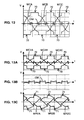
- the figure 12 represents a type of inverter arm modulation and over-modulation signals applicable to a general control component.
- MCA, MCB, MCC signals are three-phase signals with over-modulation 70 flat on the peak of the sinusoid.
- the signal OM of the general control component is determined according to the modulation signals MCA, MCB, MCC. In this case, this general component OM compensates for overmodulation to restore a sinusoidal shape by a low level modulation on the other arms.
- the figure 13A shows modulation signals MC2A, MC2B, MC2C to modulate the control arm of an inverter.
- the Figure 13B shows general control component signals OM generated according to the modulation signals of the inverter which have priority.
- the figure 13C represents modulation signals MR2A, MR2B, MR2C of a rectifier arm also having over-modulation but the forms of the voltages are not synchronized with those of the inverter.
- modulation signals of the non-priority rectifier and not forming part of the general control component saturations 71 may appear.
- the figure 14 represents signals showing an example of saturation of the arm control of a rectifier.
- the modulation signals MR2A, MR2B and MR2C are also representative of the voltage input signals of the rectifier.
- a saturation limit value Vmax a risk of saturation 71 is possible.
- the voltage Vmax is also representative or depends on the voltage of the DC voltage lines VDC or the reference voltage V2.
- Saturation values can be defined by the difference between the limit value Vmax and the values of the first modulation signals MR1A, MR1B and MR1C of the arms of the rectifier.
- the general control component can advantageously be corrected in particular according to the saturation values.
- the figure 15A shows a first general control component of OMO determined according to the first MC1A, MC1B, MC1C modulation signals of an inverter.
- the figure 15B shows an example of Vsat saturation value signals determined in function of the first general control component OMO and the first rectifier arm modulation signals MR1A, MR1B and MR1C.
- the figure 15C shows a second general control signal OM1 corrected according to the saturation value signals.
- the figure 16A shows signals MC2A, MC2B, MC2C of inverter arm modulation having corrected over-modulation with a corrected second general control component signal OM1.
- An exemplary form of a second corrected signal OM1 of a general control component is represented on the figure 16B .
- the figure 16C shows corrected modulation signals MR2A, MR2B, MR2C and limited to a maximum value Vmax as a function of the correction of the general control component.
- the Figures 17A to 17C represent signals equivalent to the signals of Figures 16A to 16C corresponding.
- the signal MC2A comprises a cropped portion 75 corresponding to the correction of the general control component OM1.
- the signal of the general control component OM1 comprises a trimmed portion 76 corresponding to the correction to eliminate or reduce the effects of saturation risks.
- the figure 17C shows in detail a limited portion of the modulation signal MR2A of a rectifier arm.
- Conversion devices may be in particular uninterruptible power supplies, variable speed drives, unidirectional or bidirectional energy converters between two electrical distribution networks that can have very different electrical characteristics, or frequency converters.
- the common neutral line LN can be connected to a ground conductor depending on the types of networks or installation protections. This LN connection may itself be a ground or ground conductor or a common reference line between the input and the output of the converter.
- the semiconductors of these converters are advantageously insulated gate transistors known as IGBTs but other types of semiconductors can be used.
- the arms may comprise several semiconductors connected in series and / or in parallel depending on the voltages, currents or electrical powers used.
- Input or output voltages can range from a few tens of volts to a thousand volts for applications in low voltage networks or have voltages of several thousand volts, particularly in medium voltage applications.
- the input or output currents can be from a few amps to over a thousand amperes.
- Another application of a converter according to the invention may be the transformation of electrical energy, in particular for medium voltage transformer replacement - low voltage, low voltage - low voltage or medium voltage - medium voltage.
Landscapes
- Engineering & Computer Science (AREA)
- Power Engineering (AREA)
- Inverter Devices (AREA)
- Rectifiers (AREA)
- Control Of Electric Motors In General (AREA)
- Dc-Dc Converters (AREA)
- Control Of Eletrric Generators (AREA)
- Ac-Ac Conversion (AREA)
- Control Of High-Frequency Heating Circuits (AREA)
Applications Claiming Priority (1)
| Application Number | Priority Date | Filing Date | Title |
|---|---|---|---|
| FR0410168A FR2875970B1 (fr) | 2004-09-27 | 2004-09-27 | Dispositif et procede de commande d'un convertisseur d'energie electrique et convertisseur comportant un tel dispositif |
Publications (2)
| Publication Number | Publication Date |
|---|---|
| EP1655827A1 EP1655827A1 (fr) | 2006-05-10 |
| EP1655827B1 true EP1655827B1 (fr) | 2010-03-03 |
Family
ID=34949035
Family Applications (1)
| Application Number | Title | Priority Date | Filing Date |
|---|---|---|---|
| EP05354033A Expired - Lifetime EP1655827B1 (fr) | 2004-09-27 | 2005-09-22 | Dispositif et procédé de commande d'un convertisseur d'énergie électrique et convertisseur comportant un tel dispositif |
Country Status (8)
| Country | Link |
|---|---|
| US (1) | US7499296B2 (da) |
| EP (1) | EP1655827B1 (da) |
| CN (1) | CN100576710C (da) |
| AT (1) | ATE460005T1 (da) |
| DE (1) | DE602005019670D1 (da) |
| DK (1) | DK1655827T3 (da) |
| ES (1) | ES2339033T3 (da) |
| FR (1) | FR2875970B1 (da) |
Cited By (1)
| Publication number | Priority date | Publication date | Assignee | Title |
|---|---|---|---|---|
| EP3939153A1 (fr) * | 2019-03-13 | 2022-01-19 | Safran | Système configuré pour délivrer un courant polyphasé de fréquence constante à partir d'une génératrice synchrone |
Families Citing this family (21)
| Publication number | Priority date | Publication date | Assignee | Title |
|---|---|---|---|---|
| US20040085046A1 (en) * | 2002-11-01 | 2004-05-06 | General Electric Company | Power conditioning system for turbine motor/generator |
| FR2880215B1 (fr) * | 2004-12-23 | 2007-02-09 | Schneider Electric Ind Sas | Dispositif et procede de commande d'un convertisseur d'energie electrique et convertisseur comportant un tel dispositif |
| RU2007149319A (ru) * | 2005-05-27 | 2009-07-10 | Сименс Энерджи Энд Отомейшн, Инк. (Us) | Функционирование инверторов с перемодуляцией |
| EP1922803B1 (de) * | 2005-09-09 | 2018-02-21 | Siemens Aktiengesellschaft | Vorrichtung für die elektroenergieübertragung |
| FR2901074B1 (fr) * | 2006-05-09 | 2008-06-13 | Schneider Electric Ind Sas | Dispositif et procede de commande d'un convertisseur et conversisseur electrique comportant un tel dispositif |
| DE102006042384B4 (de) * | 2006-09-08 | 2008-09-11 | Siemens Ag | Umrichter und Verfahren zur Steuerung eines Umrichters |
| US7800924B2 (en) * | 2007-03-27 | 2010-09-21 | Eaton Corporation | Power converter apparatus and methods using neutral coupling circuits with interleaved operation |
| EP2107672A1 (de) * | 2008-03-31 | 2009-10-07 | SMA Solar Technology AG | Dreiphasiger Wechselrichter ohne Verbindung zwischen dem Neutralleiter des Netzes und dem Mittelpunkt des Zwischenkreises |
| DE102008040144A1 (de) * | 2008-07-03 | 2010-01-07 | Robert Bosch Gmbh | Verfahren und Vorrichtung zur Optimierung einer Raumzeigerpulsweitenmodulation |
| US8030884B2 (en) * | 2009-08-31 | 2011-10-04 | General Electric Company | Apparatus for transferring energy using onboard power electronics and method of manufacturing same |
| US8421271B2 (en) * | 2009-08-31 | 2013-04-16 | General Electric Company | Apparatus for transferring energy using onboard power electronics and method of manufacturing same |
| FI122367B (fi) * | 2010-04-15 | 2011-12-30 | Abb Oy | Menetelmä ja järjestely sähkökäyttöjärjestelmän yhteydessä |
| FR2959365B1 (fr) * | 2010-04-26 | 2012-04-20 | Mge Ups Systems | Dispositif convertisseur et alimentation sans interruption equipee d'un tel dispositif |
| US9290097B2 (en) | 2010-11-05 | 2016-03-22 | Robert Louis Steigerwald | Apparatus for transferring energy using onboard power electronics with high-frequency transformer isolation and method of manufacturing same |
| US9120390B2 (en) | 2012-03-08 | 2015-09-01 | General Electric Company | Apparatus for transferring energy using onboard power electronics and method of manufacturing same |
| FR2988931B1 (fr) * | 2012-03-30 | 2015-10-16 | Schneider Toshiba Inverter | Dispositif de commande employe dans un systeme d'alimentation electrique a decoupage |
| US10958184B2 (en) * | 2014-07-09 | 2021-03-23 | Abb Schweiz Ag | Uninterruptible power supply and method of operation |
| JP5962804B1 (ja) * | 2015-03-18 | 2016-08-03 | ダイキン工業株式会社 | 電力変換器制御装置 |
| JP6461838B2 (ja) * | 2016-02-24 | 2019-01-30 | 本田技研工業株式会社 | 電源装置、機器及び制御方法 |
| GB2573318B (en) * | 2018-05-03 | 2020-06-10 | Zhong Qingchang | SYNDEM converter |
| CN115987115B (zh) * | 2023-03-21 | 2023-06-16 | 四川大学 | 一种抑制电流型pwm整流器输入电流畸变的调制方法 |
Family Cites Families (11)
| Publication number | Priority date | Publication date | Assignee | Title |
|---|---|---|---|---|
| US155893A (en) * | 1874-10-13 | Improvement in cotton-scrapers | ||
| US180379A (en) * | 1876-07-25 | Improvement in fence-posts | ||
| FR2713030B1 (fr) * | 1993-11-24 | 1996-01-12 | Merlin Gerin | Alimentation sans coupure à neutre traversant, comportant un hacheur-élévateur double. |
| US5671130A (en) * | 1996-08-23 | 1997-09-23 | Allen-Bradley Company, Inc. | Method and apparatus for controlling voltage reflections using a motor controller |
| JP3588932B2 (ja) * | 1996-09-10 | 2004-11-17 | 三菱電機株式会社 | 電力変換装置とその制御方法及びこの電力変換装置を用いた無停電電源装置 |
| US6023417A (en) * | 1998-02-20 | 2000-02-08 | Allen-Bradley Company, Llc | Generalized discontinuous pulse width modulator |
| US6271633B1 (en) * | 1999-11-01 | 2001-08-07 | Philips Electronics North America Corporation | High power factor electronic ballast with fully differential circuit topology |
| US6573664B2 (en) * | 2001-05-31 | 2003-06-03 | Koninklijke Philips Electronics N.V. | High efficiency high power factor electronic ballast |
| US6639371B2 (en) * | 2001-08-17 | 2003-10-28 | Delphi Technologies, Inc. | Method and system for controlling start of a permanent magnet machine |
| DE10156694B4 (de) * | 2001-11-17 | 2005-10-13 | Semikron Elektronik Gmbh & Co. Kg | Schaltungsanordnung |
| US6653812B1 (en) * | 2002-01-31 | 2003-11-25 | Analog Devices, Inc. | Space vector modulation methods and structures for electric-motor control |
-
2004
- 2004-09-27 FR FR0410168A patent/FR2875970B1/fr not_active Expired - Fee Related
-
2005
- 2005-09-07 US US11/219,779 patent/US7499296B2/en active Active
- 2005-09-22 AT AT05354033T patent/ATE460005T1/de not_active IP Right Cessation
- 2005-09-22 DK DK05354033.2T patent/DK1655827T3/da active
- 2005-09-22 EP EP05354033A patent/EP1655827B1/fr not_active Expired - Lifetime
- 2005-09-22 DE DE602005019670T patent/DE602005019670D1/de not_active Expired - Lifetime
- 2005-09-22 ES ES05354033T patent/ES2339033T3/es not_active Expired - Lifetime
- 2005-09-26 CN CN200510106852A patent/CN100576710C/zh not_active Expired - Lifetime
Cited By (1)
| Publication number | Priority date | Publication date | Assignee | Title |
|---|---|---|---|---|
| EP3939153A1 (fr) * | 2019-03-13 | 2022-01-19 | Safran | Système configuré pour délivrer un courant polyphasé de fréquence constante à partir d'une génératrice synchrone |
Also Published As
| Publication number | Publication date |
|---|---|
| DE602005019670D1 (de) | 2010-04-15 |
| EP1655827A1 (fr) | 2006-05-10 |
| CN1764054A (zh) | 2006-04-26 |
| US20060077701A1 (en) | 2006-04-13 |
| FR2875970A1 (fr) | 2006-03-31 |
| DK1655827T3 (da) | 2010-05-25 |
| FR2875970B1 (fr) | 2008-01-18 |
| ATE460005T1 (de) | 2010-03-15 |
| CN100576710C (zh) | 2009-12-30 |
| ES2339033T3 (es) | 2010-05-14 |
| US7499296B2 (en) | 2009-03-03 |
Similar Documents
| Publication | Publication Date | Title |
|---|---|---|
| EP1655827B1 (fr) | Dispositif et procédé de commande d'un convertisseur d'énergie électrique et convertisseur comportant un tel dispositif | |
| EP3554887B1 (fr) | Procédé de commande d'un dispositif de charge embarqué sur un véhicule électrique ou hybride | |
| US9276496B2 (en) | Power conversion apparatus including an inverter-converter combination | |
| FR2919768A1 (fr) | Procede d'alimentation de charges auxiliaires de secours, convertisseur auxiliaire et vehicule ferroviaire pour ce procede. | |
| EP1855375B1 (fr) | Dispositif et procédé de commande d'un convertisseur et convertisseur électrique comportant un tel dispositif | |
| EP2613432B1 (fr) | Compensateur d'énergie réactive et procédé d'équilibrage de tensions de demi-bus associé | |
| EP2602897B1 (fr) | Compensateur d'énergie réactive et procédé de réduction du phénomène de papillotement associé | |
| EP2815493B1 (fr) | Dispositif de conversion électrique ac/dc autorisant une récupération d'énergie et une gestion des courts-circuits côté continu et procédé de commande d'un tel dispositif | |
| EP0926807B1 (fr) | Convertisseur alternatif-continu triphasé | |
| EP0209944B1 (fr) | Dispositif statique de réglage des échanges d'énergie entre des systèmes électriques générateur et/ou récepteur | |
| EP1523088A2 (en) | Method in connection with network converter, and network converter | |
| EP1564876B1 (fr) | Poste de soudage à onduleur quasi résonnant à commutation douce | |
| EP1231704B1 (fr) | Convertisseur d'énergie | |
| EP4382343A1 (fr) | Système d'alimentation électrique alimentant une charge électrique via une tension polyphasée et en outre un réseau auxiliaire via une composante homopolaire de ladite tension, installation électrique associée | |
| WO2017072116A9 (fr) | Système de conversion de puissance bidirectionnel pour charge électrique monophasée et procédé de conversion de puissance correspondant | |
| EP1691471B1 (fr) | Dispositif et procédé de commande d'un inverseur | |
| WO2012084389A2 (fr) | Convertisseur de puissance équipé en sortie d'un dispositif de filtrage | |
| EP1873896B1 (fr) | Dispositif de conversion électrique, convertisseur et alimentation électrique sans interruption comportant un tel dispositif | |
| WO2022207571A1 (fr) | Titre : convertisseur de tension isolé | |
| FR3078212A1 (fr) | Convertisseur dc-dc pour chargeur bidirectionnel. | |
| EP3966922B1 (fr) | Convertisseur de tension multi niveaux à stockage d'énergie additionnel optimisé | |
| FR2882475A1 (fr) | Dispositif et procede de commande d'un convertisseur et convertisseur electrique comportant un tel dispositif | |
| WO2020188189A1 (fr) | Convertisseur électrique, notamment pour une intégration dans un vehicule électrique | |
| US20250226764A1 (en) | Systems and methods to reduce the dc link capacitance and improve the reliability of converters | |
| JPH0572176B2 (da) |
Legal Events
| Date | Code | Title | Description |
|---|---|---|---|
| PUAI | Public reference made under article 153(3) epc to a published international application that has entered the european phase |
Free format text: ORIGINAL CODE: 0009012 |
|
| AK | Designated contracting states |
Kind code of ref document: A1 Designated state(s): AT BE BG CH CY CZ DE DK EE ES FI FR GB GR HU IE IS IT LI LT LU LV MC NL PL PT RO SE SI SK TR |
|
| AX | Request for extension of the european patent |
Extension state: AL BA HR MK YU |
|
| RAP1 | Party data changed (applicant data changed or rights of an application transferred) |
Owner name: MGE UPS SYSTEMS |
|
| 17P | Request for examination filed |
Effective date: 20061027 |
|
| AKX | Designation fees paid |
Designated state(s): AT BE BG CH CY CZ DE DK EE ES FI FR GB GR HU IE IS IT LI LT LU LV MC NL PL PT RO SE SI SK TR |
|
| GRAP | Despatch of communication of intention to grant a patent |
Free format text: ORIGINAL CODE: EPIDOSNIGR1 |
|
| GRAS | Grant fee paid |
Free format text: ORIGINAL CODE: EPIDOSNIGR3 |
|
| GRAA | (expected) grant |
Free format text: ORIGINAL CODE: 0009210 |
|
| AK | Designated contracting states |
Kind code of ref document: B1 Designated state(s): AT BE BG CH CY CZ DE DK EE ES FI FR GB GR HU IE IS IT LI LT LU LV MC NL PL PT RO SE SI SK TR |
|
| REG | Reference to a national code |
Ref country code: GB Ref legal event code: FG4D Free format text: NOT ENGLISH |
|
| REG | Reference to a national code |
Ref country code: CH Ref legal event code: EP |
|
| REG | Reference to a national code |
Ref country code: IE Ref legal event code: FG4D |
|
| REF | Corresponds to: |
Ref document number: 602005019670 Country of ref document: DE Date of ref document: 20100415 Kind code of ref document: P |
|
| REG | Reference to a national code |
Ref country code: ES Ref legal event code: FG2A Ref document number: 2339033 Country of ref document: ES Kind code of ref document: T3 |
|
| REG | Reference to a national code |
Ref country code: DK Ref legal event code: T3 |
|
| REG | Reference to a national code |
Ref country code: NL Ref legal event code: VDEP Effective date: 20100303 |
|
| PG25 | Lapsed in a contracting state [announced via postgrant information from national office to epo] |
Ref country code: LT Free format text: LAPSE BECAUSE OF FAILURE TO SUBMIT A TRANSLATION OF THE DESCRIPTION OR TO PAY THE FEE WITHIN THE PRESCRIBED TIME-LIMIT Effective date: 20100303 |
|
| LTIE | Lt: invalidation of european patent or patent extension |
Effective date: 20100303 |
|
| PG25 | Lapsed in a contracting state [announced via postgrant information from national office to epo] |
Ref country code: LV Free format text: LAPSE BECAUSE OF FAILURE TO SUBMIT A TRANSLATION OF THE DESCRIPTION OR TO PAY THE FEE WITHIN THE PRESCRIBED TIME-LIMIT Effective date: 20100303 Ref country code: SI Free format text: LAPSE BECAUSE OF FAILURE TO SUBMIT A TRANSLATION OF THE DESCRIPTION OR TO PAY THE FEE WITHIN THE PRESCRIBED TIME-LIMIT Effective date: 20100303 Ref country code: AT Free format text: LAPSE BECAUSE OF FAILURE TO SUBMIT A TRANSLATION OF THE DESCRIPTION OR TO PAY THE FEE WITHIN THE PRESCRIBED TIME-LIMIT Effective date: 20100303 Ref country code: PL Free format text: LAPSE BECAUSE OF FAILURE TO SUBMIT A TRANSLATION OF THE DESCRIPTION OR TO PAY THE FEE WITHIN THE PRESCRIBED TIME-LIMIT Effective date: 20100303 |
|
| PG25 | Lapsed in a contracting state [announced via postgrant information from national office to epo] |
Ref country code: SE Free format text: LAPSE BECAUSE OF FAILURE TO SUBMIT A TRANSLATION OF THE DESCRIPTION OR TO PAY THE FEE WITHIN THE PRESCRIBED TIME-LIMIT Effective date: 20100303 Ref country code: RO Free format text: LAPSE BECAUSE OF FAILURE TO SUBMIT A TRANSLATION OF THE DESCRIPTION OR TO PAY THE FEE WITHIN THE PRESCRIBED TIME-LIMIT Effective date: 20100303 Ref country code: NL Free format text: LAPSE BECAUSE OF FAILURE TO SUBMIT A TRANSLATION OF THE DESCRIPTION OR TO PAY THE FEE WITHIN THE PRESCRIBED TIME-LIMIT Effective date: 20100303 Ref country code: GR Free format text: LAPSE BECAUSE OF FAILURE TO SUBMIT A TRANSLATION OF THE DESCRIPTION OR TO PAY THE FEE WITHIN THE PRESCRIBED TIME-LIMIT Effective date: 20100604 Ref country code: CY Free format text: LAPSE BECAUSE OF FAILURE TO SUBMIT A TRANSLATION OF THE DESCRIPTION OR TO PAY THE FEE WITHIN THE PRESCRIBED TIME-LIMIT Effective date: 20100303 Ref country code: EE Free format text: LAPSE BECAUSE OF FAILURE TO SUBMIT A TRANSLATION OF THE DESCRIPTION OR TO PAY THE FEE WITHIN THE PRESCRIBED TIME-LIMIT Effective date: 20100303 |
|
| PG25 | Lapsed in a contracting state [announced via postgrant information from national office to epo] |
Ref country code: CZ Free format text: LAPSE BECAUSE OF FAILURE TO SUBMIT A TRANSLATION OF THE DESCRIPTION OR TO PAY THE FEE WITHIN THE PRESCRIBED TIME-LIMIT Effective date: 20100303 Ref country code: BG Free format text: LAPSE BECAUSE OF FAILURE TO SUBMIT A TRANSLATION OF THE DESCRIPTION OR TO PAY THE FEE WITHIN THE PRESCRIBED TIME-LIMIT Effective date: 20100603 Ref country code: IS Free format text: LAPSE BECAUSE OF FAILURE TO SUBMIT A TRANSLATION OF THE DESCRIPTION OR TO PAY THE FEE WITHIN THE PRESCRIBED TIME-LIMIT Effective date: 20100703 Ref country code: SK Free format text: LAPSE BECAUSE OF FAILURE TO SUBMIT A TRANSLATION OF THE DESCRIPTION OR TO PAY THE FEE WITHIN THE PRESCRIBED TIME-LIMIT Effective date: 20100303 |
|
| PLBE | No opposition filed within time limit |
Free format text: ORIGINAL CODE: 0009261 |
|
| STAA | Information on the status of an ep patent application or granted ep patent |
Free format text: STATUS: NO OPPOSITION FILED WITHIN TIME LIMIT |
|
| PG25 | Lapsed in a contracting state [announced via postgrant information from national office to epo] |
Ref country code: PT Free format text: LAPSE BECAUSE OF FAILURE TO SUBMIT A TRANSLATION OF THE DESCRIPTION OR TO PAY THE FEE WITHIN THE PRESCRIBED TIME-LIMIT Effective date: 20100705 |
|
| 26N | No opposition filed |
Effective date: 20101206 |
|
| PG25 | Lapsed in a contracting state [announced via postgrant information from national office to epo] |
Ref country code: MC Free format text: LAPSE BECAUSE OF NON-PAYMENT OF DUE FEES Effective date: 20100930 |
|
| PG25 | Lapsed in a contracting state [announced via postgrant information from national office to epo] |
Ref country code: LU Free format text: LAPSE BECAUSE OF NON-PAYMENT OF DUE FEES Effective date: 20100922 Ref country code: HU Free format text: LAPSE BECAUSE OF FAILURE TO SUBMIT A TRANSLATION OF THE DESCRIPTION OR TO PAY THE FEE WITHIN THE PRESCRIBED TIME-LIMIT Effective date: 20100904 |
|
| PG25 | Lapsed in a contracting state [announced via postgrant information from national office to epo] |
Ref country code: TR Free format text: LAPSE BECAUSE OF FAILURE TO SUBMIT A TRANSLATION OF THE DESCRIPTION OR TO PAY THE FEE WITHIN THE PRESCRIBED TIME-LIMIT Effective date: 20100303 |
|
| REG | Reference to a national code |
Ref country code: FR Ref legal event code: PLFP Year of fee payment: 12 |
|
| REG | Reference to a national code |
Ref country code: FR Ref legal event code: PLFP Year of fee payment: 13 |
|
| REG | Reference to a national code |
Ref country code: FR Ref legal event code: PLFP Year of fee payment: 14 |
|
| PGFP | Annual fee paid to national office [announced via postgrant information from national office to epo] |
Ref country code: FI Payment date: 20240926 Year of fee payment: 20 Ref country code: DE Payment date: 20240926 Year of fee payment: 20 Ref country code: IE Payment date: 20240917 Year of fee payment: 20 |
|
| PGFP | Annual fee paid to national office [announced via postgrant information from national office to epo] |
Ref country code: DK Payment date: 20240925 Year of fee payment: 20 |
|
| PGFP | Annual fee paid to national office [announced via postgrant information from national office to epo] |
Ref country code: GB Payment date: 20240924 Year of fee payment: 20 |
|
| PGFP | Annual fee paid to national office [announced via postgrant information from national office to epo] |
Ref country code: BE Payment date: 20240925 Year of fee payment: 20 |
|
| PGFP | Annual fee paid to national office [announced via postgrant information from national office to epo] |
Ref country code: FR Payment date: 20240925 Year of fee payment: 20 |
|
| PGFP | Annual fee paid to national office [announced via postgrant information from national office to epo] |
Ref country code: IT Payment date: 20240924 Year of fee payment: 20 |
|
| PGFP | Annual fee paid to national office [announced via postgrant information from national office to epo] |
Ref country code: ES Payment date: 20241021 Year of fee payment: 20 |
|
| PGFP | Annual fee paid to national office [announced via postgrant information from national office to epo] |
Ref country code: CH Payment date: 20241001 Year of fee payment: 20 |
|
| REG | Reference to a national code |
Ref country code: DE Ref legal event code: R071 Ref document number: 602005019670 Country of ref document: DE |
|
| REG | Reference to a national code |
Ref country code: DK Ref legal event code: EUP Expiry date: 20250922 Ref country code: ES Ref legal event code: FD2A Effective date: 20250929 |
|
| REG | Reference to a national code |
Ref country code: CH Ref legal event code: PL |
|
| PG25 | Lapsed in a contracting state [announced via postgrant information from national office to epo] |
Ref country code: ES Free format text: LAPSE BECAUSE OF EXPIRATION OF PROTECTION Effective date: 20250923 |
|
| REG | Reference to a national code |
Ref country code: GB Ref legal event code: PE20 Expiry date: 20250921 |
|
| REG | Reference to a national code |
Ref country code: BE Ref legal event code: MK Effective date: 20250922 |
|
| REG | Reference to a national code |
Ref country code: IE Ref legal event code: MK9A |
|
| PG25 | Lapsed in a contracting state [announced via postgrant information from national office to epo] |
Ref country code: IE Free format text: LAPSE BECAUSE OF EXPIRATION OF PROTECTION Effective date: 20250922 |
|
| REG | Reference to a national code |
Ref country code: FI Ref legal event code: PCE Owner name: SCHNEIDER ELECTRIC IT LIMITED, IE |