EP1659557A2 - Méthode de commande d'entretien pour un panneau d'affichage plasma - Google Patents
Méthode de commande d'entretien pour un panneau d'affichage plasma Download PDFInfo
- Publication number
- EP1659557A2 EP1659557A2 EP05254127A EP05254127A EP1659557A2 EP 1659557 A2 EP1659557 A2 EP 1659557A2 EP 05254127 A EP05254127 A EP 05254127A EP 05254127 A EP05254127 A EP 05254127A EP 1659557 A2 EP1659557 A2 EP 1659557A2
- Authority
- EP
- European Patent Office
- Prior art keywords
- period
- sustain
- length
- address
- plasma display
- Prior art date
- Legal status (The legal status is an assumption and is not a legal conclusion. Google has not performed a legal analysis and makes no representation as to the accuracy of the status listed.)
- Withdrawn
Links
- 238000000034 method Methods 0.000 title claims abstract description 41
- 230000000977 initiatory effect Effects 0.000 claims description 18
- 238000011084 recovery Methods 0.000 abstract description 6
- 239000000758 substrate Substances 0.000 description 5
- 230000004888 barrier function Effects 0.000 description 4
- 238000001514 detection method Methods 0.000 description 4
- KTAVBOYXMBQFGR-MAODNAKNSA-J tetrasodium;(6r,7r)-7-[[(2z)-2-(2-amino-1,3-thiazol-4-yl)-2-methoxyimino-1-oxidoethylidene]amino]-3-[(2-methyl-5,6-dioxo-1h-1,2,4-triazin-3-yl)sulfanylmethyl]-8-oxo-5-thia-1-azabicyclo[4.2.0]oct-2-ene-2-carboxylate;heptahydrate Chemical compound O.O.O.O.O.O.O.[Na+].[Na+].[Na+].[Na+].S([C@@H]1[C@@H](C(N1C=1C([O-])=O)=O)NC(=O)\C(=N/OC)C=2N=C(N)SC=2)CC=1CSC1=NC(=O)C([O-])=NN1C.S([C@@H]1[C@@H](C(N1C=1C([O-])=O)=O)NC(=O)\C(=N/OC)C=2N=C(N)SC=2)CC=1CSC1=NC(=O)C([O-])=NN1C KTAVBOYXMBQFGR-MAODNAKNSA-J 0.000 description 4
- OAICVXFJPJFONN-UHFFFAOYSA-N Phosphorus Chemical compound [P] OAICVXFJPJFONN-UHFFFAOYSA-N 0.000 description 3
- 238000013507 mapping Methods 0.000 description 3
- 239000000203 mixture Substances 0.000 description 3
- 230000001681 protective effect Effects 0.000 description 3
- 238000009792 diffusion process Methods 0.000 description 2
- 230000009977 dual effect Effects 0.000 description 2
- CPLXHLVBOLITMK-UHFFFAOYSA-N magnesium oxide Inorganic materials [Mg]=O CPLXHLVBOLITMK-UHFFFAOYSA-N 0.000 description 2
- 239000000395 magnesium oxide Substances 0.000 description 2
- AXZKOIWUVFPNLO-UHFFFAOYSA-N magnesium;oxygen(2-) Chemical compound [O-2].[Mg+2] AXZKOIWUVFPNLO-UHFFFAOYSA-N 0.000 description 2
- 238000012986 modification Methods 0.000 description 2
- 230000004048 modification Effects 0.000 description 2
- 238000005070 sampling Methods 0.000 description 2
- 230000002459 sustained effect Effects 0.000 description 2
- 230000001360 synchronised effect Effects 0.000 description 2
- 241001270131 Agaricus moelleri Species 0.000 description 1
- 238000007599 discharging Methods 0.000 description 1
- 230000000694 effects Effects 0.000 description 1
- AMGQUBHHOARCQH-UHFFFAOYSA-N indium;oxotin Chemical compound [In].[Sn]=O AMGQUBHHOARCQH-UHFFFAOYSA-N 0.000 description 1
- 229910052751 metal Inorganic materials 0.000 description 1
- 239000002184 metal Substances 0.000 description 1
- 230000008569 process Effects 0.000 description 1
- 230000006798 recombination Effects 0.000 description 1
- 238000005215 recombination Methods 0.000 description 1
- 230000004044 response Effects 0.000 description 1
- 238000004544 sputter deposition Methods 0.000 description 1
- 239000012780 transparent material Substances 0.000 description 1
Images





Classifications
-
- G—PHYSICS
- G09—EDUCATION; CRYPTOGRAPHY; DISPLAY; ADVERTISING; SEALS
- G09G—ARRANGEMENTS OR CIRCUITS FOR CONTROL OF INDICATING DEVICES USING STATIC MEANS TO PRESENT VARIABLE INFORMATION
- G09G3/00—Control arrangements or circuits, of interest only in connection with visual indicators other than cathode-ray tubes
- G09G3/20—Control arrangements or circuits, of interest only in connection with visual indicators other than cathode-ray tubes for presentation of an assembly of a number of characters, e.g. a page, by composing the assembly by combination of individual elements arranged in a matrix no fixed position being assigned to or needed to be assigned to the individual characters or partial characters
- G09G3/22—Control arrangements or circuits, of interest only in connection with visual indicators other than cathode-ray tubes for presentation of an assembly of a number of characters, e.g. a page, by composing the assembly by combination of individual elements arranged in a matrix no fixed position being assigned to or needed to be assigned to the individual characters or partial characters using controlled light sources
- G09G3/28—Control arrangements or circuits, of interest only in connection with visual indicators other than cathode-ray tubes for presentation of an assembly of a number of characters, e.g. a page, by composing the assembly by combination of individual elements arranged in a matrix no fixed position being assigned to or needed to be assigned to the individual characters or partial characters using controlled light sources using luminous gas-discharge panels, e.g. plasma panels
- G09G3/288—Control arrangements or circuits, of interest only in connection with visual indicators other than cathode-ray tubes for presentation of an assembly of a number of characters, e.g. a page, by composing the assembly by combination of individual elements arranged in a matrix no fixed position being assigned to or needed to be assigned to the individual characters or partial characters using controlled light sources using luminous gas-discharge panels, e.g. plasma panels using AC panels
- G09G3/291—Control arrangements or circuits, of interest only in connection with visual indicators other than cathode-ray tubes for presentation of an assembly of a number of characters, e.g. a page, by composing the assembly by combination of individual elements arranged in a matrix no fixed position being assigned to or needed to be assigned to the individual characters or partial characters using controlled light sources using luminous gas-discharge panels, e.g. plasma panels using AC panels controlling the gas discharge to control a cell condition, e.g. by means of specific pulse shapes
- G09G3/294—Control arrangements or circuits, of interest only in connection with visual indicators other than cathode-ray tubes for presentation of an assembly of a number of characters, e.g. a page, by composing the assembly by combination of individual elements arranged in a matrix no fixed position being assigned to or needed to be assigned to the individual characters or partial characters using controlled light sources using luminous gas-discharge panels, e.g. plasma panels using AC panels controlling the gas discharge to control a cell condition, e.g. by means of specific pulse shapes for lighting or sustain discharge
-
- G—PHYSICS
- G09—EDUCATION; CRYPTOGRAPHY; DISPLAY; ADVERTISING; SEALS
- G09G—ARRANGEMENTS OR CIRCUITS FOR CONTROL OF INDICATING DEVICES USING STATIC MEANS TO PRESENT VARIABLE INFORMATION
- G09G3/00—Control arrangements or circuits, of interest only in connection with visual indicators other than cathode-ray tubes
- G09G3/20—Control arrangements or circuits, of interest only in connection with visual indicators other than cathode-ray tubes for presentation of an assembly of a number of characters, e.g. a page, by composing the assembly by combination of individual elements arranged in a matrix no fixed position being assigned to or needed to be assigned to the individual characters or partial characters
- G09G3/22—Control arrangements or circuits, of interest only in connection with visual indicators other than cathode-ray tubes for presentation of an assembly of a number of characters, e.g. a page, by composing the assembly by combination of individual elements arranged in a matrix no fixed position being assigned to or needed to be assigned to the individual characters or partial characters using controlled light sources
- G09G3/28—Control arrangements or circuits, of interest only in connection with visual indicators other than cathode-ray tubes for presentation of an assembly of a number of characters, e.g. a page, by composing the assembly by combination of individual elements arranged in a matrix no fixed position being assigned to or needed to be assigned to the individual characters or partial characters using controlled light sources using luminous gas-discharge panels, e.g. plasma panels
- G09G3/288—Control arrangements or circuits, of interest only in connection with visual indicators other than cathode-ray tubes for presentation of an assembly of a number of characters, e.g. a page, by composing the assembly by combination of individual elements arranged in a matrix no fixed position being assigned to or needed to be assigned to the individual characters or partial characters using controlled light sources using luminous gas-discharge panels, e.g. plasma panels using AC panels
- G09G3/291—Control arrangements or circuits, of interest only in connection with visual indicators other than cathode-ray tubes for presentation of an assembly of a number of characters, e.g. a page, by composing the assembly by combination of individual elements arranged in a matrix no fixed position being assigned to or needed to be assigned to the individual characters or partial characters using controlled light sources using luminous gas-discharge panels, e.g. plasma panels using AC panels controlling the gas discharge to control a cell condition, e.g. by means of specific pulse shapes
- G09G3/294—Control arrangements or circuits, of interest only in connection with visual indicators other than cathode-ray tubes for presentation of an assembly of a number of characters, e.g. a page, by composing the assembly by combination of individual elements arranged in a matrix no fixed position being assigned to or needed to be assigned to the individual characters or partial characters using controlled light sources using luminous gas-discharge panels, e.g. plasma panels using AC panels controlling the gas discharge to control a cell condition, e.g. by means of specific pulse shapes for lighting or sustain discharge
- G09G3/2942—Control arrangements or circuits, of interest only in connection with visual indicators other than cathode-ray tubes for presentation of an assembly of a number of characters, e.g. a page, by composing the assembly by combination of individual elements arranged in a matrix no fixed position being assigned to or needed to be assigned to the individual characters or partial characters using controlled light sources using luminous gas-discharge panels, e.g. plasma panels using AC panels controlling the gas discharge to control a cell condition, e.g. by means of specific pulse shapes for lighting or sustain discharge with special waveforms to increase luminous efficiency
-
- G—PHYSICS
- G09—EDUCATION; CRYPTOGRAPHY; DISPLAY; ADVERTISING; SEALS
- G09G—ARRANGEMENTS OR CIRCUITS FOR CONTROL OF INDICATING DEVICES USING STATIC MEANS TO PRESENT VARIABLE INFORMATION
- G09G3/00—Control arrangements or circuits, of interest only in connection with visual indicators other than cathode-ray tubes
- G09G3/20—Control arrangements or circuits, of interest only in connection with visual indicators other than cathode-ray tubes for presentation of an assembly of a number of characters, e.g. a page, by composing the assembly by combination of individual elements arranged in a matrix no fixed position being assigned to or needed to be assigned to the individual characters or partial characters
- G09G3/22—Control arrangements or circuits, of interest only in connection with visual indicators other than cathode-ray tubes for presentation of an assembly of a number of characters, e.g. a page, by composing the assembly by combination of individual elements arranged in a matrix no fixed position being assigned to or needed to be assigned to the individual characters or partial characters using controlled light sources
- G09G3/28—Control arrangements or circuits, of interest only in connection with visual indicators other than cathode-ray tubes for presentation of an assembly of a number of characters, e.g. a page, by composing the assembly by combination of individual elements arranged in a matrix no fixed position being assigned to or needed to be assigned to the individual characters or partial characters using controlled light sources using luminous gas-discharge panels, e.g. plasma panels
- G09G3/288—Control arrangements or circuits, of interest only in connection with visual indicators other than cathode-ray tubes for presentation of an assembly of a number of characters, e.g. a page, by composing the assembly by combination of individual elements arranged in a matrix no fixed position being assigned to or needed to be assigned to the individual characters or partial characters using controlled light sources using luminous gas-discharge panels, e.g. plasma panels using AC panels
- G09G3/296—Driving circuits for producing the waveforms applied to the driving electrodes
-
- G—PHYSICS
- G09—EDUCATION; CRYPTOGRAPHY; DISPLAY; ADVERTISING; SEALS
- G09G—ARRANGEMENTS OR CIRCUITS FOR CONTROL OF INDICATING DEVICES USING STATIC MEANS TO PRESENT VARIABLE INFORMATION
- G09G2310/00—Command of the display device
- G09G2310/02—Addressing, scanning or driving the display screen or processing steps related thereto
- G09G2310/0264—Details of driving circuits
- G09G2310/0275—Details of drivers for data electrodes, other than drivers for liquid crystal, plasma or OLED displays, not related to handling digital grey scale data or to communication of data to the pixels by means of a current
-
- G—PHYSICS
- G09—EDUCATION; CRYPTOGRAPHY; DISPLAY; ADVERTISING; SEALS
- G09G—ARRANGEMENTS OR CIRCUITS FOR CONTROL OF INDICATING DEVICES USING STATIC MEANS TO PRESENT VARIABLE INFORMATION
- G09G2320/00—Control of display operating conditions
- G09G2320/02—Improving the quality of display appearance
- G09G2320/0233—Improving the luminance or brightness uniformity across the screen
-
- G—PHYSICS
- G09—EDUCATION; CRYPTOGRAPHY; DISPLAY; ADVERTISING; SEALS
- G09G—ARRANGEMENTS OR CIRCUITS FOR CONTROL OF INDICATING DEVICES USING STATIC MEANS TO PRESENT VARIABLE INFORMATION
- G09G2320/00—Control of display operating conditions
- G09G2320/02—Improving the quality of display appearance
- G09G2320/0238—Improving the black level
-
- G—PHYSICS
- G09—EDUCATION; CRYPTOGRAPHY; DISPLAY; ADVERTISING; SEALS
- G09G—ARRANGEMENTS OR CIRCUITS FOR CONTROL OF INDICATING DEVICES USING STATIC MEANS TO PRESENT VARIABLE INFORMATION
- G09G2320/00—Control of display operating conditions
- G09G2320/02—Improving the quality of display appearance
- G09G2320/0247—Flicker reduction other than flicker reduction circuits used for single beam cathode-ray tubes
-
- G—PHYSICS
- G09—EDUCATION; CRYPTOGRAPHY; DISPLAY; ADVERTISING; SEALS
- G09G—ARRANGEMENTS OR CIRCUITS FOR CONTROL OF INDICATING DEVICES USING STATIC MEANS TO PRESENT VARIABLE INFORMATION
- G09G3/00—Control arrangements or circuits, of interest only in connection with visual indicators other than cathode-ray tubes
- G09G3/20—Control arrangements or circuits, of interest only in connection with visual indicators other than cathode-ray tubes for presentation of an assembly of a number of characters, e.g. a page, by composing the assembly by combination of individual elements arranged in a matrix no fixed position being assigned to or needed to be assigned to the individual characters or partial characters
- G09G3/2007—Display of intermediate tones
- G09G3/2018—Display of intermediate tones by time modulation using two or more time intervals
- G09G3/2022—Display of intermediate tones by time modulation using two or more time intervals using sub-frames
-
- G—PHYSICS
- G09—EDUCATION; CRYPTOGRAPHY; DISPLAY; ADVERTISING; SEALS
- G09G—ARRANGEMENTS OR CIRCUITS FOR CONTROL OF INDICATING DEVICES USING STATIC MEANS TO PRESENT VARIABLE INFORMATION
- G09G3/00—Control arrangements or circuits, of interest only in connection with visual indicators other than cathode-ray tubes
- G09G3/20—Control arrangements or circuits, of interest only in connection with visual indicators other than cathode-ray tubes for presentation of an assembly of a number of characters, e.g. a page, by composing the assembly by combination of individual elements arranged in a matrix no fixed position being assigned to or needed to be assigned to the individual characters or partial characters
- G09G3/22—Control arrangements or circuits, of interest only in connection with visual indicators other than cathode-ray tubes for presentation of an assembly of a number of characters, e.g. a page, by composing the assembly by combination of individual elements arranged in a matrix no fixed position being assigned to or needed to be assigned to the individual characters or partial characters using controlled light sources
- G09G3/28—Control arrangements or circuits, of interest only in connection with visual indicators other than cathode-ray tubes for presentation of an assembly of a number of characters, e.g. a page, by composing the assembly by combination of individual elements arranged in a matrix no fixed position being assigned to or needed to be assigned to the individual characters or partial characters using controlled light sources using luminous gas-discharge panels, e.g. plasma panels
- G09G3/288—Control arrangements or circuits, of interest only in connection with visual indicators other than cathode-ray tubes for presentation of an assembly of a number of characters, e.g. a page, by composing the assembly by combination of individual elements arranged in a matrix no fixed position being assigned to or needed to be assigned to the individual characters or partial characters using controlled light sources using luminous gas-discharge panels, e.g. plasma panels using AC panels
- G09G3/291—Control arrangements or circuits, of interest only in connection with visual indicators other than cathode-ray tubes for presentation of an assembly of a number of characters, e.g. a page, by composing the assembly by combination of individual elements arranged in a matrix no fixed position being assigned to or needed to be assigned to the individual characters or partial characters using controlled light sources using luminous gas-discharge panels, e.g. plasma panels using AC panels controlling the gas discharge to control a cell condition, e.g. by means of specific pulse shapes
- G09G3/292—Control arrangements or circuits, of interest only in connection with visual indicators other than cathode-ray tubes for presentation of an assembly of a number of characters, e.g. a page, by composing the assembly by combination of individual elements arranged in a matrix no fixed position being assigned to or needed to be assigned to the individual characters or partial characters using controlled light sources using luminous gas-discharge panels, e.g. plasma panels using AC panels controlling the gas discharge to control a cell condition, e.g. by means of specific pulse shapes for reset discharge, priming discharge or erase discharge occurring in a phase other than addressing
- G09G3/2922—Details of erasing
-
- G—PHYSICS
- G09—EDUCATION; CRYPTOGRAPHY; DISPLAY; ADVERTISING; SEALS
- G09G—ARRANGEMENTS OR CIRCUITS FOR CONTROL OF INDICATING DEVICES USING STATIC MEANS TO PRESENT VARIABLE INFORMATION
- G09G3/00—Control arrangements or circuits, of interest only in connection with visual indicators other than cathode-ray tubes
- G09G3/20—Control arrangements or circuits, of interest only in connection with visual indicators other than cathode-ray tubes for presentation of an assembly of a number of characters, e.g. a page, by composing the assembly by combination of individual elements arranged in a matrix no fixed position being assigned to or needed to be assigned to the individual characters or partial characters
- G09G3/22—Control arrangements or circuits, of interest only in connection with visual indicators other than cathode-ray tubes for presentation of an assembly of a number of characters, e.g. a page, by composing the assembly by combination of individual elements arranged in a matrix no fixed position being assigned to or needed to be assigned to the individual characters or partial characters using controlled light sources
- G09G3/28—Control arrangements or circuits, of interest only in connection with visual indicators other than cathode-ray tubes for presentation of an assembly of a number of characters, e.g. a page, by composing the assembly by combination of individual elements arranged in a matrix no fixed position being assigned to or needed to be assigned to the individual characters or partial characters using controlled light sources using luminous gas-discharge panels, e.g. plasma panels
- G09G3/288—Control arrangements or circuits, of interest only in connection with visual indicators other than cathode-ray tubes for presentation of an assembly of a number of characters, e.g. a page, by composing the assembly by combination of individual elements arranged in a matrix no fixed position being assigned to or needed to be assigned to the individual characters or partial characters using controlled light sources using luminous gas-discharge panels, e.g. plasma panels using AC panels
- G09G3/298—Control arrangements or circuits, of interest only in connection with visual indicators other than cathode-ray tubes for presentation of an assembly of a number of characters, e.g. a page, by composing the assembly by combination of individual elements arranged in a matrix no fixed position being assigned to or needed to be assigned to the individual characters or partial characters using controlled light sources using luminous gas-discharge panels, e.g. plasma panels using AC panels using surface discharge panels
Definitions
- the present invention relates to a driving device and method for a plasma display panel (PDP), and more particularly, to a PDD including a driving device and using a driving method to recover a data voltage drop component occurring in an address discharge.
- PDP plasma display panel
- Plasma display panel displays a picture including a character or a graphic by exciting a phosphor using an ultraviolet ray of 147nm, which is generated when an inert mixture gas such as He+Xe, Ne+Xe, or He+Ne+Xe is discharged.
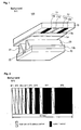
- FIG. 1 is a view illustrating a three-electrode alternate current surface discharge type PDP according to the background art.
- the three-electrode alternate current surface discharge type PDP includes a scan/sustain electrode 11a and a common sustain electrode 12a formed on an upper substrate 10, and an address electrode 22 formed on a lower substrate 20.
- Each of the scan/sustain electrode 11 a and the common sustain electrode 12a is formed of a transparent material, for example, of indium-tin-oxide (ITO).
- Metal bus electrodes 11 band 12b are formed at each of the scan/sustain electrode 11 a and the common sustain electrode 12a to reduce resistance.
- An upper dielectric layer 13a and a protective film 14 are layered on the upper substrate 10 having the scan/sustain electrode 11 a and the common sustain electrode 12a formed thereon. Wall charges are generated in plasma discharge and accumulated on the upper dielectric layer 13a.
- the protective film 14 prevents the upper dielectric layer 13a from being damaged by sputtering generated in the plasma discharge, and increases a secondary electron emission efficiency.
- the protective film 14 is formed of magnesium oxide (MgO).
- a lower dielectric layer 13b and a barrier rib 21 are formed on the lower substrate 20 having the address electrode 22 formed thereon.
- a phosphor layer 23 is coated on surfaces of the lower dielectric layer 13b and the barrier rib 21.
- the address electrode 22 is formed in a direction of intersecting with the scan/sustain electrode 11 a and the common sustain electrode 12a.
- the barrier rib 21 is formed in parallel with the address electrode 22, thereby preventing ultraviolet ray and visible ray, which are generated in the plasma discharge, from being leaked to an adjacent discharge cell.
- the phosphor layer 23 is excited by the ultraviolet ray to generate any one of red, green and blue visible light.
- the inert mixture gas such as He+Xe, Ne+Xe or He+Ne+Xe is injected into a discharge space of the discharge cell for discharge.
- the discharge space is provided between the upper and lower substrates 10 and 20 and the barrier rib 21.
- FIG. 2 illustrates the method of expressing the image scale of the PDP of FIG. 1.
- the image grayscale is expressed with one frame divided into various sub-fields each sub-field having different light emission times.
- Each of the sub-fields is divided into a reset period for uniformly generating discharge, an address period for selecting the discharge cell, and a sustain period for embodying the grayscale depending on discharge times.
- a frame period (16.67ms) corresponding to 1/60 second is divided into eight sub-fields.
- Each of the eight sub-fields is again divided into a reset period, an address period and a sustain period.
- This increase in the sustain period is fixed and implemented automatically independent of any signal/voltage characteristics of the PDP.
- a driving waveform of the PDP driven with the divided sub-fields will be described as follows referring to FIG. 3.
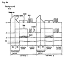
- FIG. 3 illustrates the waveform for describing the driving method for the PDP according to the background art.
- the PDP is driven by dividing a sub-field into an initialization/reset period for initializing an entire picture, an address period for selecting a cell, and a sustain period for sustaining a discharge of the selected cell.
- a ramp-up waveform (Ramp-up) is concurrently supplied to all scan electrodes (Y).
- the ramp-up waveform causes the discharge in cells of the entire picture.
- positive (+) wall charges are accumulated on the address electrode (X) and the sustain electrode (Z), and negative (-) wall charges are accumulated on the scan electrode (Y).
- a ramp-down waveform (Ramp-down) is supplied at a setdown period (SD) to generate a weak erasure discharge, thereby partially erasing excessive wall charges.
- the ramp-down waveform begins to drop from a positive voltage lower than the peak voltage of the ramp-up waveform to a ground voltage (GND) or a specific positive voltage level.
- GND ground voltage
- the wall charges are uniformly remained within the cells to stably generate an address discharge.
- a negative scan pulse (scan) is sequentially supplied to the scan electrodes (Y) and at the same time, a positive data pulse (data) is supplied to the address electrodes (X) in synchronization with the scan pulse (scan).
- a voltage difference between the scan pulse and the data pulse is summed with a wall voltage generated during the initialization period
- the address discharge is generated within the cell to which the data pulse (Dp) is supplied.
- the wall charges are formed within the cells selected by the address discharge to generate the discharge at the time of applying a sustain voltage.
- a positive direct current voltage (Zdc) is supplied to the sustain electrode (Z) to reduce a voltage difference between the sustain electrode (Z) and the scan electrode (Y) at the setdown period and the address period. By doing so, an erroneous discharge is prevented between the sustain electrode (Z) and the scan electrode (Y).
- a sustain pulse (sus) is supplied alternately to the scan electrodes (Y) and the sustain electrodes (Z). While the wall voltage of the cell is summed with the sustain pulse (sus), a sustain discharge (that is, a display discharge) is generated between the scan electrode (Y) and the sustain electrode (Z) at the cell, which is selected through the address discharge, whenever the sustain pulse (sus) is supplied.
- a ramp waveform (erase) having a small pulse width and voltage level is supplied to the sustain electrode (Z) to erase the wall charges remaining within the cells of the entire picture.
- a voltage of the data pulse i.e., the level of the data voltage Vd supplied to a data electrode X as the data pulse
- the discharge pattern means a pattern of data or a data pattern established by 0's and 1's.
- the switching time refers to a number of switchings from 0 to 1 or 1 to 0 within the data supplied to the data electrodes.
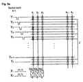
- FIGS. 4a - 5b illustrate data voltage characteristics depending on the discharge pattern of the discharge cell of a PDP according to the background art.
- FIGS. 4a and 4b illustrate the data voltage (Vd) characteristic at the address period when the discharge cell belonging to one line (e.g., X1) of the data electrode is continuously discharged, that is, when switching times for supplying the data pulse Dp (Data) are small.
- FIGS. 5a and 5b illustrate the data voltage (Vd) characteristic at the address period when the discharge cell belonging to one line (e.g., X1) of the data electrode is noncontinuously and irregularly discharged, that is, when the switching times for supplying the data pulse Dp to the line X1 are large.
- the data voltage (Vd) supplied to the data electrode X1 may drop slightly during the address period as shown in FIG. 4b.
- the voltage (Vd) supplied to the data electrode heavily drops during the address period as shown in FIG. 5b.
- this drawback is more prominent in the PDP using a single scan method.
- the switching load increases due to a longer line length of the data electrodes, which in turn causes an increase in the amount of data voltage drop for the data electrodes.
- the erroneous discharge is easily caused due to the loss of the wall charge, because a motion of a spatial charge is activated within the cell and a recombination is easily generated.
- an object of the present invention is to solve at least the above and other problems and disadvantages of the background art.
- Another object of the present invention is to provide a driving device and method for a plasma display panel in which when the plasma display panel is driven, the sustain periods are varied depending on certain characteristics, thereby providing a stable discharge characteristic without an erroneous discharge.
- Another object of the present invention is to provide a plasma display device including a plasma display panel and a driving part for driving the plasma display panel, which overcome the limitations and disadvantages associated with the background art.
- a plasma display apparatus being driven by dividing a sub-field into at least an address period and a sustain period, the apparatus comprising: a timing controlling unit to vary a length of the sustain period according to a data pattern associated with at least one address electrode.
- a plasma display apparatus being driven by dividing a sub-field into at least an address period and a sustain period, the apparatus comprising: a timing controlling unit to adjust a length of the sustain period according to an amount of a switching load of an address electrode.
- a plasma display apparatus being driven by dividing a sub-field into at least an address period and a sustain period, the apparatus comprising: a timing controlling unit to adjust a length of the sustain period according to an amount of drop in a data voltage during the address period.
- a driving method for a plasma display apparatus being driven by dividing a sub-field into at least an address period and a sustain period, the method comprising: varying a length of the sustain period according to a data pattern associated with at least one address electrode.
- a driving method for a plasma display apparatus being driven by dividing a sub-field into at least an address period and a sustain period, the method comprising: varying a length of the sustain period according to an amount of a switching load of an address electrode.
- a driving method for a plasma display apparatus being driven by dividing a sub-field into at least an address period and a sustain period, the method comprising: varying a length of the sustain period according to an amount of drop in a data voltage during the address period.
- the present invention has an effect in that when the plasma display panel is driven, a recovery period of a data pulse voltage is sufficiently provided in the sustain period to provide a stable discharge characteristic at each of the sub-fields without an erroneous discharge where the discharge of the discharge cell is turned off.
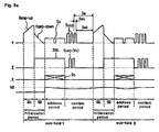
- FIGS. 6a and 6b are views illustrating a data voltage characteristic and a waveform for describing a driving method for a plasma display panel according to the present invention.
- the plasma display panel is driven by dividing each sub-field of a frame into a reset/initialization period for initializing an entire picture, an address period for selecting a cell, and a sustain period for sustaining the discharge of the selected cell.
- a ramp-up waveform (Ramp-up) is concurrently supplied to all scan electrodes (Y).
- 0 [V] is supplied to a sustain electrode (Z) and an address electrode (X).
- the ramp-up waveform causes a write dark discharge not almost generating light between the scan electrode (Y) and the address electrode (X) and between the scan electrode (Y) and the sustain electrode (Z) within cells of the entire picture.
- the write dark discharge positive (+) wall charges are accumulated on the address electrode (X) and the sustain electrode (Z), and negative (-) wall charges are accumulated on the scan electrode (Y).
- a ramp-down waveform (Ramp-down) is concurrently supplied to the scan electrodes (Y) at a setdown period (SD).
- the ramp-down waveform begins to drop from a positive voltage lower than the peak voltage of the ramp-up waveform to a ground voltage (GND) or a specific positive voltage level.
- a sustain voltage (Vs) in the form of pulses (Susp) is supplied to the sustain electrode (Z), and 0 [V] is supplied to the address electrode (X).
- a scan pulse (Sp) is sequentially supplied to the scan electrodes (Y) and at the same time, a data pulse (Dp) is supplied sequentially to the address electrodes (X) in synchronization with the scan pulse (Sp). While a voltage difference between the scan pulse (Sp) and the data pulse (Dp) is summed with a wall voltage generated during the reset period, the address discharge is generated within the cell to which the data pulse (Dp) is supplied.
- the address discharge can be performed in a dual scan method or a single scan method. In the dual scan method, the address discharge is respectively and independently performed in the plasma display panel divided into upper and lower parts. In the single scan method, the address discharge is performed at one time in the entire of the plasma display panel. Meantime, the positive direct voltage (Zdc) is supplied to the sustain electrode (Z) during the address period.
- a sustain pulse (Susp) of the sustain voltage (Vs) is alternately supplied to the scan electrodes (Y) and the sustain electrodes (Z). While the wall voltage of the cell is summed with a voltage of the sustain pulse (Susp), a sustain discharge (that is, a display discharge) is generated between the scan electrode (Y) and the sustain electrode (Z) at the cell, which is selected through the address discharge, whenever the sustain pulse (Susp) is supplied.
- the sustain period is varied by a controlling unit (e.g., a timing controller 121 in FIG. 7) depending on an amount of drop in the data voltage Vd applied to the address electrode (X). The data voltage drop amount is generated in the address discharge during the address period.
- the timing controlling unit in the driving device of the PDP controls to lengthen the sustain period as the data voltage drop amount is increased.
- the present invention provides a sufficient time during the sustain period of a current sub-field to recover the drop in the data voltage during the address period of the current sub-field, so that a stable discharge can be performed in the next sub-field.
- the data voltage drop can be generated by various causes, but is mostly generated due to an increase in the switching load.
- the switching load is generated when a switching element of the address electrode (X) is switched on or off to write data in a necessary one of all cells of the plasma display panel. Accordingly, the present invention varies the length of the sustain period depending on the switching load amount
- the length of the sustain period can be controlled depending on the data voltage drop amount in different ways, for example, by varying a length of a supply period and a ground sustain period of a sustain pulse generating a first sustain discharge, or a length of a supply period and a ground sustain period of a sustain pulse generating other sustain discharge, among a plurality of sustain pulses supplied during the sustain period.
- it is desirable that the sustain period is controlled by varying a length of a period (Sw) from a start time point of a last sustain pulse of a current sub-field to a reset period start time point of a next sub-field.
- the period (Sw) extending from the initiation time point of the last sustain pulse supplied at the scan electrode (Y) in a current sub-field to the reset period start time point of the next sub-field can be varied in the range of 100 ⁇ s to 1 ms.
- the period Sw is made up of a supply period (Swa) and a ground period (SWb).
- the supply period (Swa) of the last sustain pulse for generating the last sustain discharge is a minimal period enough to generate the sustain discharge. Therefore, the supply period (Swa) has at least 1 ⁇ s.
- it is desirable that the supply period (Swa) is controlled to be at or less than 1 ms in consideration of a limited period from the sustain period initiation time point of the last sustain pulse to the reset period time point of the next sub-field.
- the sustain pulse (Susp) can have a sustain waveform, wherein a last sustain pulse is supplied during a minute width period or the same width period as that of a previously supplied sustain pulse and is sustained to the ground level (GND) during the remaining part of the sustain period.
- the length of the sustain period is varied by varying the length of the ground period (SWb) of the last sustain pulse.
- the length of such ground period (SWb) may be varied within the range of 100 ⁇ s-1ms.
- the sustain pulse (Sp) can have a sustain waveform, wherein the last sustain pulse seems to be sustained to the sustain voltage (Vs) until the reset period start time point of the next sub-field. That is, in this case, the length of the sustain period is varied by varying the length of the supply period (SWa) of the last sustain pulse.
- the length of such supply period (SWa) may be varied within the range of 1 ⁇ s-1 ms.
- a minimal critical value of 100 ⁇ s or more is to sufficiently recover the data voltage, which drops at the address period, until before the address period of the next sub-field when the plasma display panel is driven.
- a maximal critical value of 1 ms or less is to secure an operation margin of the sustain period when the plasma display panel is driven.
- the inventive driving method for the plasma display panel can be applied to any one or more sub-fields in the plasma display panel driven through a combination of a plurality of sub-fields, to control the sustain period depending on the data voltage drop amount.
- the inventive driving method for the plasma display panel can be applied to at least any one sub-field to control the sustain period depending on the data voltage drop amount.
- the present invention can sufficiently recover the data voltage drop amount of the address period during the sustain period to suppress the erroneous discharge, thereby preventing the discharge cell from being turned off when a write discharge is performed to write data during the address period of the next sub-field. Accordingly, a stable discharge can be performed at all of the sub-fields.
- FIG. 7 is a view illustrating a plasma display panel having a drive device according to an embodiment of the present invention.
- the driving method according to the present invention as discussed above and below can be implemented in the device of FIG. 7 or other suitable device.
- the inventive driving device of the plasma display panel 130 includes a data driving unit 122 for supplying data to the address electrodes (X1 to Xm) of a panel 128; a scan driving unit 123 for driving the scan electrodes (Y1 to Yn); a sustain driving unit 124 for driving the sustain electrodes (Z) being common electrodes; a timing controlling unit 121 for controlling the data driving unit 122, the scan driving unit 123 and the sustain driving unit 124; and a driving voltage generating unit 125 for supplying a driving voltage necessary for each of the driving units 122, 123 and 124. All the components of the PDP including the driving device are operatively coupled.
- Video data is inputted from the exterior to an inverse gamma correction unit (not shown) and an error diffusion unit (not shown) for inverse gamma correction and error diffusion. This process is known.
- the inputted video data is mapped to each of the sub-fields through a sub-field mapping unit 120.
- the sub-field mapping unit 120 supplies the mapped data to the data driving unit 122 and to the timing controlling unit 121.
- the data driving unit 122 samples and latches the received data in response to a timing control signal (CTRX) of the timing controlling unit 121 and then, supplies the latched data to the address electrodes (X1 to Xm).
- CTRX timing control signal
- the scan driving unit 123 supplies the ramp-up waveform and the ramp-down waveform to the scan electrodes (Y1 to Yn) during the reset period under the control of the timing controlling unit 121. Further, the scan driving unit 123 sequentially supplies the scan pulse (Sp) of the scan voltage (Vy) to the scan electrodes (Y1 to Yn) during the address period under the control of the timing controlling unit 121. The scan driving unit 123 supplies the sustain pulse (Susp) of the sustain voltage (Vs), which is controlled depending on the data voltage drop amount determined in the timing controlling unit 121, to the scan electrodes (Y1 to Yn) during the sustain period.
- the sustain driving unit 124 is controlled under the control of the timing controlling unit 121 to supply a bias voltage of the sustain voltage (Vs) to the sustain electrodes (Z) during the address period and a period for generating the ramp-down waveform. Further, the sustain driving unit 124 is operated alternately with the scan driving unit 123 during the sustain period to supply the sustain pulse (Susp) to the sustain electrodes (Z). Further, the sustain driving unit 124 can also supply the erasure ramp waveform (Vramp-ers) to the sustain electrodes (Z) if the last sustain discharge is finished at one sub-field.
- the timing controlling unit 121 receives vertical and horizontal synchronous signals and a clock signal, and generates timing control signals (e.g., CTRX, CTRY and CTRZ) to control each of the driving units 122, 123 and 124.
- the timing controlling unit 121 supplies the timing control signals (CTRX, CTRY and CTRZ) respectively to the corresponding driving units 122, 123 and 124 to control an operation of each of the driving units 122, 123 and 124.
- the timing controlling unit 121 includes a detecting unit 121a; however, the detecting unit 121a can be separately provided from the timing controlling unit 121.
- the detecting unit 121a can be an independent entity or can be part of another element in the device, e.g., the data driving unit 122.
- the detecting unit 121a detects a data voltage drop amount, which is generated in plasma discharge at the address period, by using data allocated to each of the sub-fields in the sub-field mapping unit 120.
- the drop in the data voltage can be detected by, e.g., examining the data voltage at the data/address electrode(s). As the data voltage drop increases, the length of the period Sw of the sustain period may be increased.
- the detecting unit 121 a can detect an amount of switching load, e.g., by detecting a number of switchings between 0's and 1's in the data supplied to the data electrode(s). As the switching number increases, the length of the period Sw may increase.
- the detecting unit 121 a can detect a data pattern of the data supplied to the data electrode(s). By detecting the data pattern, a number of switchings between 0's and 1's in the data pattern is detected. As the number of switchings increases, the length of the period Sw may increase.
- the timing controlling unit 121 generates a control signal corresponding to the data voltage drop amount (or the switching load or the data pattern) detected in the amount detecting unit 121a, to supply the generated control signal to the scan driving unit 123.
- the switching load is generated depending on the discharge pattern of the discharge cell.
- the discharge pattern is determined depending on a pattern of data (data pattern) inputted to the data driving unit 122.
- control signal corresponding to the detection by the detecting unit 121 a controls the length of the sustain period and preferably, controls the period from the sustain period initiation time point of the last sustain pulse to the reset period time point of the next sub-field.
- this period is controlled, e.g., it is lengthened by the timing controlling unit 121 as the data voltage drop amount is increased.
- the period from the sustain initiation time point of the last sustain pulse to the reset period time point of the next sub-field can be controlled to be within the range of 100 ⁇ s to 1 ms.
- the period from the sustain initiation time point of the last sustain pulse to the reset period time point of the next sub-field is controlled to be within the range of 100 ⁇ s to 1 ms.
- the minimal critical value of 100 ⁇ s or more is to sufficiently recover the data voltage, which drops at the address period, until before the address period of the next sub-field when the plasma display panel is driven.
- the maximal critical value of 1 ms or less is to secure the operation margin of the sustain period when the plasma display panel is driven.
- the supply period of the sustain pulse for generating the last sustain discharge is a minimal period enough to generate the sustain discharge. Therefore, the supply period has at least 1 ⁇ s. However, it is desirable that the supply period is controlled to be less than 1 ms in consideration of the limited period from the sustain period initiation time point of the last sustain pulse to the reset period time point of the next sub-field.
- the inventive driving method of controlling the sustain period depending on the data voltage drop amount (or switching load or data pattern) is applied to the plasma display panel for generating the address discharge in a single scan method, a data voltage recovery efficiency is more increased.
- the inventive driving method for the plasma display panel can be applied to only any one single sub-field in the plasma display panel, which is driven through the combination of the plurality of sub-fields, to control the sustain period depending on the detection by the detecting unit 121a.
- the inventive driving method for the plasma display panel can be applied to all of the plurality of sub-fields or at least any one sub-field to control the sustain period depending on the detection by the detecting unit 121a (i.e., data voltage drop amount, switching load, or a data pattern).
- the inventive driving method can be applied to at least one sub-field to control the sustain period.
- the inventive driving method is applied only to front half sub-fields (SF1, SF2 and SF3) of the plasma display panel, which is driven with at least eight sub-fields, to control the sustain period in consideration of a sustain driving margin and a jittering phenomenon occurring during the address period.
- the data control signal includes a sampling clock for sampling the data, a latch control signal, and a switch control signal for controlling a turn-on/off time of the driving switching element and an energy recovery circuit.
- the scan control signal includes a switch control signal for controlling a turn-on/off time of a driving switching element and an energy recovery circuit, which are installed in the scan driving unit 123.
- the sustain control signal (CTRZ) includes a switch control signal for controlling a turn-on/off time of a driving switching element and an energy recovery circuit, which are installed in the sustain driving unit 124.
- the driving voltage generating unit 125 generates a setup voltage (Vsetup), a scan common voltage (Vscan-com), the scan voltage (-Vy), the sustain voltage (Vs), the data voltage (Vd) and the like. These driving voltages can be varied depending on a composition of a discharge gas or a structure of the discharge cell.
Landscapes
- Engineering & Computer Science (AREA)
- Physics & Mathematics (AREA)
- Power Engineering (AREA)
- Plasma & Fusion (AREA)
- Computer Hardware Design (AREA)
- General Physics & Mathematics (AREA)
- Theoretical Computer Science (AREA)
- Control Of Indicators Other Than Cathode Ray Tubes (AREA)
- Control Of Gas Discharge Display Tubes (AREA)
Applications Claiming Priority (1)
| Application Number | Priority Date | Filing Date | Title |
|---|---|---|---|
| KR1020040096019A KR20060056820A (ko) | 2004-11-22 | 2004-11-22 | 플라즈마 디스플레이 패널 구동장치 및 구동방법 |
Publications (2)
| Publication Number | Publication Date |
|---|---|
| EP1659557A2 true EP1659557A2 (fr) | 2006-05-24 |
| EP1659557A3 EP1659557A3 (fr) | 2006-07-05 |
Family
ID=35929781
Family Applications (1)
| Application Number | Title | Priority Date | Filing Date |
|---|---|---|---|
| EP05254127A Withdrawn EP1659557A3 (fr) | 2004-11-22 | 2005-06-30 | Méthode de commande d'entretien pour un panneau d'affichage plasma |
Country Status (6)
| Country | Link |
|---|---|
| US (1) | US7911421B2 (fr) |
| EP (1) | EP1659557A3 (fr) |
| JP (1) | JP4253647B2 (fr) |
| KR (1) | KR20060056820A (fr) |
| CN (1) | CN100437693C (fr) |
| TW (1) | TWI308317B (fr) |
Families Citing this family (7)
| Publication number | Priority date | Publication date | Assignee | Title |
|---|---|---|---|---|
| KR100739636B1 (ko) * | 2005-07-06 | 2007-07-13 | 삼성에스디아이 주식회사 | 플라즈마 표시 장치 및 그 구동 방법 |
| KR100666106B1 (ko) * | 2005-07-16 | 2007-01-09 | 엘지전자 주식회사 | 플라즈마 디스플레이 장치 |
| WO2007139039A1 (fr) | 2006-05-26 | 2007-12-06 | Nec Corporation | dispositif de classement d'informations, procÉdÉ de classement d'informations et programme de classement d'informations |
| JP5228317B2 (ja) * | 2006-12-07 | 2013-07-03 | パナソニック株式会社 | プラズマディスプレイ装置およびプラズマディスプレイパネルの駆動方法 |
| US8421714B2 (en) * | 2006-12-28 | 2013-04-16 | Panasonic Corporation | Plasma display device and method for driving plasma display panel |
| CN103903552A (zh) * | 2014-03-14 | 2014-07-02 | 四川虹欧显示器件有限公司 | 一种等离子显示器驱动方法 |
| CN103903551A (zh) * | 2014-03-14 | 2014-07-02 | 四川虹欧显示器件有限公司 | 一种等离子显示器驱动方法 |
Citations (2)
| Publication number | Priority date | Publication date | Assignee | Title |
|---|---|---|---|---|
| EP1347435A2 (fr) | 2002-03-20 | 2003-09-24 | Fujitsu Hitachi Plasma Display Limited | Appareil d'affichage |
| EP1457960A2 (fr) | 2003-03-11 | 2004-09-15 | LG Electronics Inc. | Méthode de commande d'un panneau d'affichage à plasma |
Family Cites Families (8)
| Publication number | Priority date | Publication date | Assignee | Title |
|---|---|---|---|---|
| US6100859A (en) * | 1995-09-01 | 2000-08-08 | Fujitsu Limited | Panel display adjusting number of sustaining discharge pulses according to the quantity of display data |
| JPH1039831A (ja) | 1996-07-22 | 1998-02-13 | Matsushita Electric Ind Co Ltd | ディスプレイの駆動回路と表示装置 |
| JP3573968B2 (ja) | 1997-07-15 | 2004-10-06 | 富士通株式会社 | プラズマディスプレイの駆動方法及び駆動装置 |
| EP1020838A1 (fr) | 1998-12-25 | 2000-07-19 | Pioneer Corporation | Procédé de commande d'un panneau d'affichage à plasma |
| JP5077860B2 (ja) | 2001-05-31 | 2012-11-21 | 株式会社日立プラズマパテントライセンシング | Pdpの駆動方法および表示装置 |
| JP4308488B2 (ja) * | 2002-03-12 | 2009-08-05 | 日立プラズマディスプレイ株式会社 | プラズマディスプレイ装置 |
| JP2004004513A (ja) | 2002-04-25 | 2004-01-08 | Fujitsu Hitachi Plasma Display Ltd | プラズマディスプレイパネルの駆動方法およびプラズマディスプレイ装置 |
| JP4100338B2 (ja) | 2002-12-13 | 2008-06-11 | 松下電器産業株式会社 | プラズマディスプレイパネルの駆動方法 |
-
2004
- 2004-11-22 KR KR1020040096019A patent/KR20060056820A/ko not_active Ceased
-
2005
- 2005-06-22 TW TW094120767A patent/TWI308317B/zh not_active IP Right Cessation
- 2005-06-27 US US11/166,118 patent/US7911421B2/en not_active Expired - Fee Related
- 2005-06-29 CN CNB2005100823086A patent/CN100437693C/zh not_active Expired - Fee Related
- 2005-06-30 EP EP05254127A patent/EP1659557A3/fr not_active Withdrawn
- 2005-06-30 JP JP2005192217A patent/JP4253647B2/ja not_active Expired - Fee Related
Patent Citations (2)
| Publication number | Priority date | Publication date | Assignee | Title |
|---|---|---|---|---|
| EP1347435A2 (fr) | 2002-03-20 | 2003-09-24 | Fujitsu Hitachi Plasma Display Limited | Appareil d'affichage |
| EP1457960A2 (fr) | 2003-03-11 | 2004-09-15 | LG Electronics Inc. | Méthode de commande d'un panneau d'affichage à plasma |
Also Published As
| Publication number | Publication date |
|---|---|
| CN100437693C (zh) | 2008-11-26 |
| US7911421B2 (en) | 2011-03-22 |
| EP1659557A3 (fr) | 2006-07-05 |
| JP4253647B2 (ja) | 2009-04-15 |
| US20060109207A1 (en) | 2006-05-25 |
| CN1779760A (zh) | 2006-05-31 |
| TW200617853A (en) | 2006-06-01 |
| JP2006146148A (ja) | 2006-06-08 |
| KR20060056820A (ko) | 2006-05-25 |
| TWI308317B (en) | 2009-04-01 |
Similar Documents
| Publication | Publication Date | Title |
|---|---|---|
| US7583241B2 (en) | Plasma display apparatus and driving method of the same | |
| EP1596412A2 (fr) | Appareil d'affichage à plasma et méthode de commande | |
| US20060103594A1 (en) | Plasma display apparatus and method of driving the same | |
| EP1736956A1 (fr) | Appareil d'affichage à plasma et procédé de commande correspondant | |
| US7911421B2 (en) | Driving device and method for plasma display panel | |
| CN100414584C (zh) | 等离子显示面板的驱动方法及其装置 | |
| EP1677279A2 (fr) | Appareil d'affichage plasma et son procédé de commande | |
| US20060103593A1 (en) | Plasma display apparatus and method of driving the same | |
| US7564430B2 (en) | Plasma display apparatus and driving method thereof | |
| KR20070051208A (ko) | 플라즈마 디스플레이 장치 | |
| JP2006011459A5 (fr) | ||
| CN100458890C (zh) | 等离子显示设备及其驱动方法 | |
| JP2006235574A (ja) | プラズマディスプレイ装置、その駆動方法、プラズマディスプレイパネル及びプラズマディスプレイパネルの駆動装置 | |
| JP2006011459A (ja) | プラズマディスプレイ装置及びその駆動方法 | |
| US20070069986A1 (en) | Plasma display apparatus and driving method thereof | |
| KR100645783B1 (ko) | 플라즈마 표시장치 및 그 구동방법 | |
| KR100761166B1 (ko) | 플라즈마 디스플레이 장치 및 그의 구동 방법 | |
| KR100508256B1 (ko) | 플라즈마 디스플레이 패널의 구동방법 및 장치 | |
| EP1744298A1 (fr) | Appareil d'affichage à plasma et procédé de commande correspondant | |
| EP1775697A2 (fr) | Appareil d'affichage à plasma | |
| US7619586B2 (en) | Plasma display apparatus and method for driving the same | |
| EP1669973A2 (fr) | Appareil d'affichage à plasma | |
| KR100793292B1 (ko) | 플라즈마 디스플레이 장치 및 그의 구동 방법 | |
| EP1696412A2 (fr) | Panneau d'affichage à plasma, appareil d'affichage à plasma, appareil de commande de ce panneau et procédé de commande de cet appareil | |
| EP1679686A1 (fr) | Appareil d'affichage à plasma et son procédé de commande |
Legal Events
| Date | Code | Title | Description |
|---|---|---|---|
| PUAI | Public reference made under article 153(3) epc to a published international application that has entered the european phase |
Free format text: ORIGINAL CODE: 0009012 |
|
| AK | Designated contracting states |
Kind code of ref document: A2 Designated state(s): AT BE BG CH CY CZ DE DK EE ES FI FR GB GR HU IE IS IT LI LT LU MC NL PL PT RO SE SI SK TR |
|
| AX | Request for extension of the european patent |
Extension state: AL BA HR LV MK YU |
|
| PUAL | Search report despatched |
Free format text: ORIGINAL CODE: 0009013 |
|
| AK | Designated contracting states |
Kind code of ref document: A3 Designated state(s): AT BE BG CH CY CZ DE DK EE ES FI FR GB GR HU IE IS IT LI LT LU MC NL PL PT RO SE SI SK TR |
|
| AX | Request for extension of the european patent |
Extension state: AL BA HR LV MK YU |
|
| 17P | Request for examination filed |
Effective date: 20060711 |
|
| 17Q | First examination report despatched |
Effective date: 20061206 |
|
| AKX | Designation fees paid |
Designated state(s): DE FR GB NL |
|
| STAA | Information on the status of an ep patent application or granted ep patent |
Free format text: STATUS: THE APPLICATION IS DEEMED TO BE WITHDRAWN |
|
| 18D | Application deemed to be withdrawn |
Effective date: 20121115 |