EP1347435A2 - Appareil d'affichage - Google Patents
Appareil d'affichage Download PDFInfo
- Publication number
- EP1347435A2 EP1347435A2 EP02257655A EP02257655A EP1347435A2 EP 1347435 A2 EP1347435 A2 EP 1347435A2 EP 02257655 A EP02257655 A EP 02257655A EP 02257655 A EP02257655 A EP 02257655A EP 1347435 A2 EP1347435 A2 EP 1347435A2
- Authority
- EP
- European Patent Office
- Prior art keywords
- sustain discharge
- pulse
- display apparatus
- pulse width
- discharge pulse
- Prior art date
- Legal status (The legal status is an assumption and is not a legal conclusion. Google has not performed a legal analysis and makes no representation as to the accuracy of the status listed.)
- Granted
Links
- 238000000034 method Methods 0.000 claims abstract description 75
- 238000010586 diagram Methods 0.000 description 12
- 230000007423 decrease Effects 0.000 description 4
- 230000000750 progressive effect Effects 0.000 description 3
- 230000015556 catabolic process Effects 0.000 description 2
- 230000010354 integration Effects 0.000 description 2
- 238000004519 manufacturing process Methods 0.000 description 2
- 238000006731 degradation reaction Methods 0.000 description 1
- 230000017525 heat dissipation Effects 0.000 description 1
- 239000004973 liquid crystal related substance Substances 0.000 description 1
- 239000011159 matrix material Substances 0.000 description 1
- 230000004044 response Effects 0.000 description 1
- 230000007704 transition Effects 0.000 description 1
- 238000003079 width control Methods 0.000 description 1
Images




Classifications
-
- G—PHYSICS
- G09—EDUCATION; CRYPTOGRAPHY; DISPLAY; ADVERTISING; SEALS
- G09G—ARRANGEMENTS OR CIRCUITS FOR CONTROL OF INDICATING DEVICES USING STATIC MEANS TO PRESENT VARIABLE INFORMATION
- G09G3/00—Control arrangements or circuits, of interest only in connection with visual indicators other than cathode-ray tubes
- G09G3/20—Control arrangements or circuits, of interest only in connection with visual indicators other than cathode-ray tubes for presentation of an assembly of a number of characters, e.g. a page, by composing the assembly by combination of individual elements arranged in a matrix no fixed position being assigned to or needed to be assigned to the individual characters or partial characters
- G09G3/22—Control arrangements or circuits, of interest only in connection with visual indicators other than cathode-ray tubes for presentation of an assembly of a number of characters, e.g. a page, by composing the assembly by combination of individual elements arranged in a matrix no fixed position being assigned to or needed to be assigned to the individual characters or partial characters using controlled light sources
- G09G3/28—Control arrangements or circuits, of interest only in connection with visual indicators other than cathode-ray tubes for presentation of an assembly of a number of characters, e.g. a page, by composing the assembly by combination of individual elements arranged in a matrix no fixed position being assigned to or needed to be assigned to the individual characters or partial characters using controlled light sources using luminous gas-discharge panels, e.g. plasma panels
- G09G3/288—Control arrangements or circuits, of interest only in connection with visual indicators other than cathode-ray tubes for presentation of an assembly of a number of characters, e.g. a page, by composing the assembly by combination of individual elements arranged in a matrix no fixed position being assigned to or needed to be assigned to the individual characters or partial characters using controlled light sources using luminous gas-discharge panels, e.g. plasma panels using AC panels
- G09G3/296—Driving circuits for producing the waveforms applied to the driving electrodes
-
- G—PHYSICS
- G09—EDUCATION; CRYPTOGRAPHY; DISPLAY; ADVERTISING; SEALS
- G09G—ARRANGEMENTS OR CIRCUITS FOR CONTROL OF INDICATING DEVICES USING STATIC MEANS TO PRESENT VARIABLE INFORMATION
- G09G3/00—Control arrangements or circuits, of interest only in connection with visual indicators other than cathode-ray tubes
- G09G3/20—Control arrangements or circuits, of interest only in connection with visual indicators other than cathode-ray tubes for presentation of an assembly of a number of characters, e.g. a page, by composing the assembly by combination of individual elements arranged in a matrix no fixed position being assigned to or needed to be assigned to the individual characters or partial characters
- G09G3/2007—Display of intermediate tones
- G09G3/2018—Display of intermediate tones by time modulation using two or more time intervals
- G09G3/2022—Display of intermediate tones by time modulation using two or more time intervals using sub-frames
-
- G—PHYSICS
- G09—EDUCATION; CRYPTOGRAPHY; DISPLAY; ADVERTISING; SEALS
- G09G—ARRANGEMENTS OR CIRCUITS FOR CONTROL OF INDICATING DEVICES USING STATIC MEANS TO PRESENT VARIABLE INFORMATION
- G09G3/00—Control arrangements or circuits, of interest only in connection with visual indicators other than cathode-ray tubes
- G09G3/20—Control arrangements or circuits, of interest only in connection with visual indicators other than cathode-ray tubes for presentation of an assembly of a number of characters, e.g. a page, by composing the assembly by combination of individual elements arranged in a matrix no fixed position being assigned to or needed to be assigned to the individual characters or partial characters
- G09G3/22—Control arrangements or circuits, of interest only in connection with visual indicators other than cathode-ray tubes for presentation of an assembly of a number of characters, e.g. a page, by composing the assembly by combination of individual elements arranged in a matrix no fixed position being assigned to or needed to be assigned to the individual characters or partial characters using controlled light sources
- G09G3/28—Control arrangements or circuits, of interest only in connection with visual indicators other than cathode-ray tubes for presentation of an assembly of a number of characters, e.g. a page, by composing the assembly by combination of individual elements arranged in a matrix no fixed position being assigned to or needed to be assigned to the individual characters or partial characters using controlled light sources using luminous gas-discharge panels, e.g. plasma panels
- G09G3/288—Control arrangements or circuits, of interest only in connection with visual indicators other than cathode-ray tubes for presentation of an assembly of a number of characters, e.g. a page, by composing the assembly by combination of individual elements arranged in a matrix no fixed position being assigned to or needed to be assigned to the individual characters or partial characters using controlled light sources using luminous gas-discharge panels, e.g. plasma panels using AC panels
- G09G3/291—Control arrangements or circuits, of interest only in connection with visual indicators other than cathode-ray tubes for presentation of an assembly of a number of characters, e.g. a page, by composing the assembly by combination of individual elements arranged in a matrix no fixed position being assigned to or needed to be assigned to the individual characters or partial characters using controlled light sources using luminous gas-discharge panels, e.g. plasma panels using AC panels controlling the gas discharge to control a cell condition, e.g. by means of specific pulse shapes
- G09G3/294—Control arrangements or circuits, of interest only in connection with visual indicators other than cathode-ray tubes for presentation of an assembly of a number of characters, e.g. a page, by composing the assembly by combination of individual elements arranged in a matrix no fixed position being assigned to or needed to be assigned to the individual characters or partial characters using controlled light sources using luminous gas-discharge panels, e.g. plasma panels using AC panels controlling the gas discharge to control a cell condition, e.g. by means of specific pulse shapes for lighting or sustain discharge
-
- G—PHYSICS
- G09—EDUCATION; CRYPTOGRAPHY; DISPLAY; ADVERTISING; SEALS
- G09G—ARRANGEMENTS OR CIRCUITS FOR CONTROL OF INDICATING DEVICES USING STATIC MEANS TO PRESENT VARIABLE INFORMATION
- G09G3/00—Control arrangements or circuits, of interest only in connection with visual indicators other than cathode-ray tubes
- G09G3/20—Control arrangements or circuits, of interest only in connection with visual indicators other than cathode-ray tubes for presentation of an assembly of a number of characters, e.g. a page, by composing the assembly by combination of individual elements arranged in a matrix no fixed position being assigned to or needed to be assigned to the individual characters or partial characters
- G09G3/22—Control arrangements or circuits, of interest only in connection with visual indicators other than cathode-ray tubes for presentation of an assembly of a number of characters, e.g. a page, by composing the assembly by combination of individual elements arranged in a matrix no fixed position being assigned to or needed to be assigned to the individual characters or partial characters using controlled light sources
- G09G3/28—Control arrangements or circuits, of interest only in connection with visual indicators other than cathode-ray tubes for presentation of an assembly of a number of characters, e.g. a page, by composing the assembly by combination of individual elements arranged in a matrix no fixed position being assigned to or needed to be assigned to the individual characters or partial characters using controlled light sources using luminous gas-discharge panels, e.g. plasma panels
- G09G3/288—Control arrangements or circuits, of interest only in connection with visual indicators other than cathode-ray tubes for presentation of an assembly of a number of characters, e.g. a page, by composing the assembly by combination of individual elements arranged in a matrix no fixed position being assigned to or needed to be assigned to the individual characters or partial characters using controlled light sources using luminous gas-discharge panels, e.g. plasma panels using AC panels
- G09G3/291—Control arrangements or circuits, of interest only in connection with visual indicators other than cathode-ray tubes for presentation of an assembly of a number of characters, e.g. a page, by composing the assembly by combination of individual elements arranged in a matrix no fixed position being assigned to or needed to be assigned to the individual characters or partial characters using controlled light sources using luminous gas-discharge panels, e.g. plasma panels using AC panels controlling the gas discharge to control a cell condition, e.g. by means of specific pulse shapes
- G09G3/294—Control arrangements or circuits, of interest only in connection with visual indicators other than cathode-ray tubes for presentation of an assembly of a number of characters, e.g. a page, by composing the assembly by combination of individual elements arranged in a matrix no fixed position being assigned to or needed to be assigned to the individual characters or partial characters using controlled light sources using luminous gas-discharge panels, e.g. plasma panels using AC panels controlling the gas discharge to control a cell condition, e.g. by means of specific pulse shapes for lighting or sustain discharge
- G09G3/2946—Control arrangements or circuits, of interest only in connection with visual indicators other than cathode-ray tubes for presentation of an assembly of a number of characters, e.g. a page, by composing the assembly by combination of individual elements arranged in a matrix no fixed position being assigned to or needed to be assigned to the individual characters or partial characters using controlled light sources using luminous gas-discharge panels, e.g. plasma panels using AC panels controlling the gas discharge to control a cell condition, e.g. by means of specific pulse shapes for lighting or sustain discharge by introducing variations of the frequency of sustain pulses within a frame or non-proportional variations of the number of sustain pulses in each subfield
-
- G—PHYSICS
- G09—EDUCATION; CRYPTOGRAPHY; DISPLAY; ADVERTISING; SEALS
- G09G—ARRANGEMENTS OR CIRCUITS FOR CONTROL OF INDICATING DEVICES USING STATIC MEANS TO PRESENT VARIABLE INFORMATION
- G09G2360/00—Aspects of the architecture of display systems
- G09G2360/16—Calculation or use of calculated indices related to luminance levels in display data
Definitions
- the present invention relates to a display apparatus and a method for driving the same, and more particularly to a display apparatus, such as a plasma display panel (PDP), that repeatedly carries out sustain discharges having sustain discharge pulses (light emission pulses) and adjusts the emission of light based on the number of repetitions, and a method for driving such a display apparatus.
- a display apparatus such as a plasma display panel (PDP)
- PDP plasma display panel
- thin display apparatuses With the recent trend toward larger-screen displays, the need for thin display apparatuses has been increasing, and various types of thin display apparatus have been commercially implemented. Examples include matrix panels that display images by directly using digital signals, such as PDPs and other gas discharge display panels, digital micromirror devices (DMDs), EL display devices, fluorescent display tubes, and liquid crystal display devices.
- DMDs digital micromirror devices
- EL display devices EL display devices
- fluorescent display tubes fluorescent display tubes
- liquid crystal display devices liquid crystal display devices.
- gas discharge display panels are considered to be the most promising candidate for large-area, direct-view HDTV (high-definition television) display devices, because of the simple production process which facilitates fabrication of larger-area displays, a self-luminescent property which ensures good display quality, and a high response speed.
- one field is divided into a plurality of light emission blocks (subfields: SFs) each comprising a plurality of sustain discharge pulses, and a grayscale is displayed by combining these subfields. That is, the PDP achieves a grayscale display by repeating sustain discharges with sustain discharge pulses and thereby adjusting the light emission time.
- subfields SFs
- a grayscale is displayed by combining these subfields. That is, the PDP achieves a grayscale display by repeating sustain discharges with sustain discharge pulses and thereby adjusting the light emission time.
- the current (sustain discharge current) is initially small, but gradually increases toward the end of the sustain discharge period as the sustain discharge is repeated. Since power is consumed by the sustain discharge, the sustain discharge voltage decreases in a manner that is inversely proportional to the current, and this decrease of the sustain discharge voltage results in an incomplete sustain discharge; accordingly, there is a need for a display apparatus that can perform control considering the sustain voltage drop when displaying an image that consumes much power, and also a need for a method for driving such a display apparatus.
- field is used by assuming the case of interlaced scanning in which one image frame is made up of two fields, an odd field and an even field, but in the case of progressive scanning in which one image frame is made up of one field, the term “field” can be used interchangeably with "frame”.
- sustain discharge pulses are set, for example, by calculating a display load ratio for each frame from display data and by performing computation based on the display load ratio for each frame (field) so that the power consumption of the display apparatus will not exceed a predetermined value.
- Such techniques are disclosed, for example, in Japanese Unexamined Patent Publication (Kokai) Nos. 06-332397 and 2000-098970.
- Japanese Unexamined Patent Publication (Kokai) No. 06-332397 discloses a flat panel display apparatus comprising an integrating means for integrating the number of pixel signals of a prescribed level applied during a prescribed period, and a frequency changing means for changing the panel driving frequency based on the result of the integration of the intearating means
- Japanese Unexamined Patent Publication (Kokai) No. 2000-098970 discloses a plasma display apparatus comprising an integrating means for integrating, for each bit signal used to achieve grayscale display, the number of pixel signals applied during a prescribed period, and a frequency changing means for changing the frequency of a sustain discharge waveform, based on the result of the integration of the integrating means.
- a driving method for a display apparatus that produces light emission by applying a sustain discharge pulse repeatedly, wherein a pulse width of the sustain discharge pulse is varied within one subfield and is controlled in accordance with the amount of voltage drop of a sustain discharge voltage.
- the sustain discharge voltage may be actually detected, and the pulse width of the sustain discharge pulse may be controlled in accordance with the detected sustain discharge voltage.
- a load ratio of a plurality of subfields forming one filed may be detected, and the pulse width of the sustain discharge pulse may be controlled in accordance with the detected subfield load ratio.
- a weighted average load ratio of one entire field may be calculated, and the pulse width of the sustain discharge pulse may be controlled in accordance with the calculated weighted average load ratio.
- a driving method for a display apparatus that produces light emission by applying a sustain discharge pulse repeatedly, wherein a pulse width of the sustain discharge pulse is varied within one subfield, and control is performed by making the pulse width of the sustain discharge pulse narrow in a first half of a sustain discharge period and wide in a second half thereof.
- a driving method for a display apparatus that produces light emission by applying a sustain discharge pulse repeatedly, wherein a pulse width of the sustain discharge pulse is varied within one subfield, and control is performed so that the pulse width of the sustain discharge pulse is narrow in an early part of a sustain discharge period, but gradually increases toward the end of the sustain discharge period.
- a driving method for a display apparatus that produces light emission by applying a sustain discharge pulse repeatedly, wherein a pulse width of the sustain discharge pulse is varied within one subfield, and control is performed so that the pulse width of the sustain discharge pulse is narrow in a specific part within the subfield, but gradually increases after the specific part within the subfield.
- the pulse width of the sustain discharge pulse may be controlled so that at least a first pulse in the sustain discharge period has a wide pulse width.
- the total number of sustain discharge pulses in one entire field may be calculated, and the pulse width of the sustain discharge pulse may be controlled in accordance with the calculated total number of sustain discharge pulses.
- the pulse width of every one of the sustain discharge pulses in the all subfields may be made wider.
- the one field may be made up of a plurality of subfields, and a grayscale may be displayed by combining the subfields.
- the display apparatus may be a plasma display apparatus.
- a display apparatus comprising a display panel section; a data converter which receives an image signal and supplies image data suitable for the display apparatus to the display panel section; a power supply section which supplies power to the display panel section; and a sustain discharge pulse control circuit which varies a pulse width of sustain discharge pulse within one subfield and controls the pulse width of the sustain discharge pulse in accordance with the amount of voltage drop of a sustain discharge voltage.
- the power supply section may actually detect the sustain discharge voltage, and the sustain discharge pulse control circuit may control the pulse width of the sustain discharge pulse in accordance with the detected sustain discharge voltage.
- the data converter may detect a load ratio of each of the subfields forming one field, and the sustain discharge pulse control circuit may control the pulse width of the sustain discharge pulse in accordance with the detected load ratio of the each subfield.
- the data converter may calculate a weighted average load ratio of one entire field, and the sustain discharge pulse control circuit may control the pulse width of the sustain discharge pulse in accordance with the calculated weighted average load ratio.
- a display apparatus comprising a display panel section; a data converter which receives an image signal and supplies image data suitable for the display apparatus to the display panel section; a power supply section which supplies power to the display panel section; and a sustain discharge pulse control circuit which varies a pulse width of sustain discharge pulse within one subfield and performs control by making the pulse width of the sustain discharge pulse narrow in a first half of a sustain discharge period and wide in a second half thereof.
- a display apparatus comprising a display panel section; a data converter which receives an image signal and supplies image data suitable for the display apparatus to the display panel section; a power supply section which supplies power to the display panel section; and a sustain discharge pulse control circuit which varies a pulse width of sustain discharge pulse within one subfield and performs control so that the pulse width of the sustain discharge pulse is narrow in an early part of a sustain discharge period, but gradually increases toward the end of the sustain discharge period.
- a display apparatus comprising a display panel section; a data converter which receives an image signal and supplies image data suitable for the display apparatus to the display panel section; a power supply section which supplies power to the display panel section; and a sustain discharge pulse control circuit which varies a pulse width of sustain discharge pulse within one subfield and performs control so that the pulse width of the sustain discharge pulse is narrow in a specific part within the subfield, but gradually increases after the specific part within the subfield.
- the sustain discharge pulse control circuit may control the pulse width of the sustain discharge pulse so that at least a first pulse in the sustain discharge period has a wide pulse width.
- the display apparatus may further comprise a power control circuit which adjusts the number of sustain discharge pulses by receiving a display load ratio from the data converter and information from the power supply section about power being consumed in the display panel section, and wherein the power control circuit may calculate the number of sustain discharge pulses in one entire field, and the sustain discharge pulse control circuit may control the pulse width of the sustain discharge pulse in accordance with the calculated number of sustain discharge pulses.
- the calculated total number of sustain discharge pulses may be smaller than the number of sustain discharge pulses whose pulse width is made identically wider in all subfields, and when the number of sustain discharge pulses in each of the subfields is smaller than the number of pulses having an off time that makes the pulse width of every sustain discharge pulse wider, the sustain discharge pulse control circuit may make the pulse width of every one of the sustain discharge pulses in the all subfields wider.
- the one field may be made up of a plurality of subfields, and the display apparatus may display a grayscale by combining the subfields.
- the display apparatus may be a plasma display apparatus.
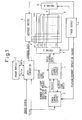
- FIG. 1 is a block diagram showing one example of a display apparatus to which the present invention is applied; here, one example of a plasma display apparatus (plasma display panel: PDP) is illustrated.
- reference numeral 1 is a data converter
- 2 is a frame memory
- 3 is a power control circuit
- 4 is a driver control circuit
- 5 is a power supply
- 6 is an address driver
- 7 is a Y driver
- 8 is an X driver
- 9 is a display panel.
- the data converter 1 receives an image signal and a vertical synchronization signal Vsync from the outside, and converts them into PDP display data (data for displaying an image using a plurality of subfields SFs).
- the frame memory 2 holds the PDP display data converted by the data converter 1 and to be used in the next field.
- the data converter 1 then reads the data previously held in the frame memory 2 and supplies it as address data to the address driver 6, while at the same time, providing its display load ratio to the driver control circuit 4.
- the display load ratio is found by counting the number of cells to be excited (dots to be illuminated) in each subfield.
- the driver control circuit 4 receives from the power control circuit 3 a control signal for controlling the number of sustain discharge pulses (sustain pulses) for each subfield (SF) and an internally generated vertical synchronization signal Vsync2, and supplies drive control data to the Y driver 7.
- the data signal of the display load ratio, output from the data converter 1, is supplied to the power control circuit 3 via the driver control circuit 4.
- the display panel 9 includes address electrodes A1 to Am, Y electrodes Y1 to Yn, and X electrodes X, which are driven by the address driver 6, the Y driver 7, and the X driver 8, respectively.
- the address driver 6, the Y driver 7, the X driver 8, and the display panel 9 together constitute the display panel section.
- Figure 2 is a diagram for explaining one example of a driving method for the display apparatus shown in Figure 1.
- the driving method shown in Figure 2 displays one image frame by interlacing two fields, an odd field and an even field, and the odd field and the even field are each made up of a plurality of subfields (for example, seven subfields SF0 to SF6).
- Each of the subfields SF0 to SF6 has an address discharge period, during which address discharge is performed to excite cells in accordance with the address data, and a sustain discharge period (light emission period), during which sustain discharge pulses (light emission pulses) are applied to the selected cells (illuminated cells) to sustain the light emission state.
- Figure 3 is a diagram for explaining another example of the driving method for the display apparatus shown in Figure 1.
- the driving method shown in Figure 3 displays one image frame by progressive scanning in a single field, and the field (frame) is made up of a plurality of subfields (for example, six subfields SF0 to SF5).
- Each of the subfields SF0 to SF5 has an address discharge period, during which address discharge is performed to excite cells in accordance with the address data, and a sustain discharge period, during which sustain discharge pulses are applied to the selected cells to sustain the light emission state.
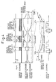
- Figure 4 is a diagram for explaining one example of a prior art display apparatus driving method, showing the relationships between the sustain discharge voltage Vs, sustain discharge current Is, and sustain discharge pulse period Tsus (Tsus0, Tsus1, Tsus2).
- the sustain discharge current Is begins to gradually increase from the start position SDs of the period and, inversely proportional to it, the sustain discharge voltage Vs gradually decreases.
- the sustain discharge current Is reaches a maximum value at the end position SDe of the sustain discharge period Tsus (Tsus1), while the sustain discharge voltage Vs reaches a minimum value at the end position SDe of the sustain discharge period Tsus (Tsus1).
- the sustain discharge pulse width is constant (for example, 2 ⁇ s) throughout the sustain discharge period Tsus (Tsus1).
- the number of sustain discharge pulses must be increased, but if the number of sustain discharge pulses is increased, the sustain discharge voltage Vs further drops.
- the sustain discharge voltage Vs is raised, there arise various problems in terms of the breakdown voltage of driver circuitry, heat dissipation, power consumption, etc., and in reality, the sustain discharge voltage Vs cannot be set high enough. Accordingly, in the prior art display apparatus, the voltage drop of the sustain discharge voltage Vs has resulted in insufficient sustain discharge, and hence degradation in display quality.
- Embodiments of the display apparatus and its driving method according to the present invention will be described in detail below with reference to drawings.
- the display apparatus and its driving method according to the present invention are not limited in application to interlaced scan PDPs, but can be applied widely to various other display apparatuses, including progressive scan PDPs.
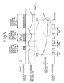
- Figure 5 is a diagram for explaining one embodiment of the display apparatus driving method according to the present invention.
- the sustain discharge pulse with is varied within one subfield (for example, SF1), rather than raising the sustain discharge voltage Vs by considering the amount of its voltage drop.
- the amount of drop (voltage drop) of the sustain discharge voltage Vs within one subfield SF1 differs at different positions in the sustain discharge period Tsus1. More specifically, the voltage level of the sustain discharge voltage Vs begins to gradually decrease from the start position SDs of the sustain discharge period Tsus1, and reaches a minimum value at the end position SDe of the sustain discharge period Tsus1.
- the pulse width (the width of the sustain discharge voltage level of the sustain discharge pulse) is set narrow (for example, 1 ⁇ s) at positions near the start position SDs of the sustain discharge period Tsus1, and the pulse width is increased (for example, to 2 ⁇ m) at positions in the middle, and is further increased (for example, to 3 ⁇ m) at positions near the end position SDe of the sustain discharge period Tsus1, compensating for the voltage drop of the sustain discharge voltage Vs by thus increasing the sustain discharge pulse width.
- the pulse widths among which the sustain discharge pulse width is varied within one subfield are not limited to the above three pulse widths (1 ⁇ s, 2 ⁇ s, and 3 ⁇ s).
- the sustain discharge pulse width within one subfield can be controlled in such a manner that it is narrow in the first half of the sustain discharge period Tsus but wide in the second half of the sustain discharge period, or in such a manner that it is initially narrow but gradually becomes wide toward the end of the sustain discharge period Tsus.
- the display apparatus driving method of this embodiment increases the sustain discharge pulse width, thereby allowing a sufficient wall charge to be formed even with a low sustain discharge voltage and thus achieving complete sustain discharge.
- the display load ratio of the entire field (frame) becomes large, the number of sustain discharge pulses is reduced to reduce the power consumption.
- the resulting off period is diverted to the sustain discharge period so that sustain discharge pulses of wider pulse width can be applied at positions where the sustain discharge current is large; in this way, a high display quality can be maintained even when the display load varies.
- the display apparatus driving method of this embodiment it becomes possible to maintain a high display quality by compensating for incomplete sustain discharge resulting from the voltage drop of the sustain discharge voltage, without having to raise the voltage level of the sustain discharge voltage.
- FIG. 6 is a flowchart showing one example of the display apparatus driving method according to the present invention, in which the sustain discharge pulse width is controlled in accordance with the total number of sustain discharge pulses in one field.
- WAL weighted average load ratio
- step ST105 the subfield SF count value n is set to 0, and in step ST106, the calculated number, S, of sustain discharge pulses is compared with the number, A, of sustain discharge pulses whose pulse width can be made wider identically in all the subfields SF.
- step ST106 If it is determined in step ST106 that the relation S ⁇ A holds, the process proceeds to step ST113 where the count value n is compared with the number of subfields SF. If it is determined in step ST113 that the relation n ⁇ N does not hold, that is, the count value n has not yet reached the largest weight subfield SFn, then in step ST114 the count value, m, of the number of sustain discharge pulses in each subfield SF is set to 0, and in step ST115, m is compared with M ⁇ SF(n) ⁇ .
- M ⁇ SF(*) ⁇ indicates the number of pulses in the subfield SF(*) that have an off time that can make the pulse width of every sustain discharge pulse wider.
- step ST115 If it is determined in step ST115 that the relation m ⁇ M ⁇ SF(n) ⁇ does not hold, the process proceeds to step ST116 where P ⁇ SF(n), m ⁇ is set to P3 (wide sustain discharge pulse width), and then in step ST117, m is incremented by 1, after which the process returns to step ST115.
- P ⁇ SF(*), m ⁇ indicates the output pulse width of the sustain discharge pulse in the subfield SF(*).
- step ST115 If it is determined in step ST115 that the relation m ⁇ M ⁇ SF(n) ⁇ holds, the process proceeds to step ST118 where the count value n is incremented by 1, after which the process returns to step ST113 to repeat the same process as described above. Then, if it is determined in step ST113 that the relation n ⁇ N holds, that is, the count value n has reached the largest weight subfield SFn, the process is terminated.
- a change point at which the sustain discharge pulse width is changed is provided, thus setting a threshold value defining the number of sustain discharge pulse repetitions at which the pulse width is changed.
- the threshold value must be set according to the total number of sustain discharge pulses in each field (frame), and the change point determined for each subfield SF according to the total number of sustain discharge pulses in that field is maintained in a look-up table (LUT).
- Figure 6 illustrates an example in which two change points (T1 and T2) are provided for adjusting the sustain discharge pulse width, and a description will be given by focusing attention on a particular subfield SF.
- step ST106 If it is determined in step ST106 that the relation S ⁇ A does not hold, the process proceeds to step ST107 where n is compared with the number of subfields SF. If it is determined in step ST107 that the relation n ⁇ N does not hold, that is, the count value n has not yet reached the largest weight subfield SFn, the process proceeds to step ST108 where T1 ⁇ SF(n) ⁇ and T2 ⁇ SF(n) ⁇ are determined from the look-up table (LUT) based on the calculated number, S, of sustain discharge pulses.
- LUT look-up table
- T1 ⁇ SF(*) ⁇ is a timing parameter defining the timing for changing the pulse width in the subfield SF(*), and determines the number of sustain discharge pulse repetitions reaching which data is changed to P3 (wide sustain discharge pulse width).
- T2 ⁇ SF(*) ⁇ is a timing parameter defining the timing for changing the pulse width in the subfield SF(*), and determines the number of sustain discharge pulse repetitions reaching which data is changed to P2 (intermediate sustain discharge pulse width).
- step ST109 the count value m is set to 0, and in step ST110, m is compared with T1. If it is determined in step ST110 that m ⁇ T1 does not hold, then P ⁇ SF(n), m ⁇ is set to P1 (narrow sustain discharge pulse width) in step ST111, and m is incremented by 1 in step ST112, after which the process returns to step ST110.
- step ST110 If it is determined in step ST110 that m ⁇ T1 holds, the process proceeds to step ST119 to carry out the steps ST119 to ST121 corresponding to the steps ST110 to ST112. That is, if it is determined in step ST119 that m ⁇ T2 does not hold, then P ⁇ SF(n), m ⁇ is set to P2 (intermediate sustain discharge pulse width) in step ST120, and m is incremented by 1 in step ST121, after which the process returns to step ST119.
- step ST119 If it is determined in step ST119 that m ⁇ T2 holds, the process proceeds to step ST122 to carry out the steps ST122 to ST124 corresponding to the steps ST110 to ST112 (steps ST119 to ST121). That is, if it is determined in step ST122 that m ⁇ M ⁇ SF(n) ⁇ does not hold, then P ⁇ SF(n), m ⁇ is set to P3 (wide sustain discharge pulse width) in step ST123, and m is incremented by 1 in step ST124, after which the process returns to step ST122.
- step ST122 determines whether m ⁇ M ⁇ SF(n) ⁇ holds. If it is determined in step ST122 that m ⁇ M ⁇ SF(n) ⁇ holds, the process proceeds to step ST125 where n is incremented by 1, after which the process returns to step ST107 to repeat the same process as described above.
- the pulse width in the subfield SF(n) is set to P1 (narrow sustain discharge pulse width) for the first to (T1 ⁇ SF(n) ⁇ - 1)th sustain discharge pulses in the sustain discharge period (Tsus), to P2 (intermediate sustain discharge pulse width) for the (T1 ⁇ SF(n) ⁇ + 1)th to (T2 ⁇ SF(n) ⁇ - 1)th sustain discharge pulses in the sustain discharge period (Tsus), and to P3 (wide sustain discharge pulse width) for all subsequent pulses. That is, the respective sustain discharge pulse widths are defined by the relation P1 ⁇ P2 ⁇ P3.
- the number of change points T1, T2 can be increased as desired; this can be accomplished by setting additional change points (T3, ..., Tk) and adding a matching number of pulse width determining loops similar to those performed using the change points T1 and T2 in the flowchart of Figure 6.
- step ST107 if it is determined in step ST107 that the relation n ⁇ N holds, that is, the count value n has reached the largest weight subfield SFn, the process is terminated.
- Figure 7 is a flowchart showing another example of the display apparatus driving method according to the present invention, in which the sustain discharge pulse width is controlled in accordance with the load ratio of each of the subfields forming one field.
- T1 ⁇ SF(n) ⁇ and T2 ⁇ SF(n) ⁇ are determined in step ST108 from the look-up table (LUT) based on the total number, S, of sustain discharge pulses in one field
- the driving method of this example shown in Figure 7 determines T1 ⁇ SF(n) ⁇ and T2 ⁇ SF(n) ⁇ in step ST208 from the look-up table (LUT) based on the load ratio L ⁇ SF(n) ⁇ of each of the subfields forming one field. Otherwise, the process is the same as that shown in Figure 6, and will not be further described here.
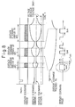
- Figure 8 is a diagram for explaining another embodiment of the display apparatus driving method according to the present invention.
- the display apparatus driving method of this embodiment performs control in such a manner as to increase the pulse width of the first sustain discharge pulse (for example, to 4 ⁇ s) in the sustain discharge period Tsus (Tsus1) in each subfield (for example, subfield SF1), thereby ensuring reliable transition from the address discharge to the sustain discharge.
- the configuration sustain discharge pulse width control
- control is performed to increase the pulse width of the first sustain discharge pulse in the sustain discharge period Tsus, but this need not be limited to the first pulse; for example, control may be performed to increase the pulse width of the first two or three sustain discharge pulses.
- a display apparatus capable of maintaining a high display quality without depending on display ratio can be provided, along with a method for driving such a display apparatus.
Landscapes
- Engineering & Computer Science (AREA)
- Physics & Mathematics (AREA)
- Computer Hardware Design (AREA)
- General Physics & Mathematics (AREA)
- Theoretical Computer Science (AREA)
- Power Engineering (AREA)
- Plasma & Fusion (AREA)
- Control Of Indicators Other Than Cathode Ray Tubes (AREA)
- Control Of Gas Discharge Display Tubes (AREA)
- Transforming Electric Information Into Light Information (AREA)
Applications Claiming Priority (2)
| Application Number | Priority Date | Filing Date | Title |
|---|---|---|---|
| JP2002078791 | 2002-03-20 | ||
| JP2002078791A JP4612985B2 (ja) | 2002-03-20 | 2002-03-20 | プラズマディスプレイ装置の駆動方法 |
Publications (3)
| Publication Number | Publication Date |
|---|---|
| EP1347435A2 true EP1347435A2 (fr) | 2003-09-24 |
| EP1347435A3 EP1347435A3 (fr) | 2004-12-22 |
| EP1347435B1 EP1347435B1 (fr) | 2012-01-18 |
Family
ID=27785304
Family Applications (1)
| Application Number | Title | Priority Date | Filing Date |
|---|---|---|---|
| EP02257655A Expired - Lifetime EP1347435B1 (fr) | 2002-03-20 | 2002-11-05 | Appareil d'affichage à plasma et son procédé de commande en mode sous-trame |
Country Status (6)
| Country | Link |
|---|---|
| US (1) | US6891519B2 (fr) |
| EP (1) | EP1347435B1 (fr) |
| JP (1) | JP4612985B2 (fr) |
| KR (2) | KR20030076189A (fr) |
| CN (1) | CN1271585C (fr) |
| TW (1) | TWI277927B (fr) |
Cited By (2)
| Publication number | Priority date | Publication date | Assignee | Title |
|---|---|---|---|---|
| EP1659557A2 (fr) | 2004-11-22 | 2006-05-24 | Lg Electronics Inc. | Méthode de commande d'entretien pour un panneau d'affichage plasma |
| EP2045795A3 (fr) * | 2007-10-01 | 2010-04-07 | Samsung SDI Co., Ltd. | Affichage à plasma et procédé de commande associé |
Families Citing this family (26)
| Publication number | Priority date | Publication date | Assignee | Title |
|---|---|---|---|---|
| JP2003140605A (ja) * | 2001-08-24 | 2003-05-16 | Sony Corp | プラズマ表示装置及びその駆動方法 |
| KR100490542B1 (ko) * | 2002-11-26 | 2005-05-17 | 삼성에스디아이 주식회사 | 어드레스기간과 유지기간의 혼합 방식으로 동작하는패널구동방법 및 그 장치 |
| JP4619014B2 (ja) | 2003-03-28 | 2011-01-26 | 株式会社日立製作所 | プラズマディスプレイパネルの駆動方法 |
| KR100515299B1 (ko) | 2003-04-30 | 2005-09-15 | 삼성에스디아이 주식회사 | 화상 표시 장치와 그 표시 패널 및 구동 방법 |
| JP4385117B2 (ja) * | 2003-07-17 | 2009-12-16 | パナソニック株式会社 | プラズマディスプレイパネルの駆動方法 |
| JP4084262B2 (ja) * | 2003-08-08 | 2008-04-30 | 三星エスディアイ株式会社 | 輝度補正回路、輝度補正方法及び映像表示装置並びに映像表示方法 |
| JP4399638B2 (ja) | 2003-10-02 | 2010-01-20 | 株式会社日立プラズマパテントライセンシング | プラズマディスプレイパネルの駆動方法 |
| KR20050075216A (ko) * | 2004-01-16 | 2005-07-20 | 엘지전자 주식회사 | 플라즈마 표시 패널에서의 로드 이펙트 상쇄 장치 |
| JP4647220B2 (ja) * | 2004-03-24 | 2011-03-09 | 日立プラズマディスプレイ株式会社 | プラズマディスプレイ装置の駆動方法 |
| JP4860117B2 (ja) * | 2004-05-21 | 2012-01-25 | 日立プラズマディスプレイ株式会社 | 表示装置 |
| KR100681021B1 (ko) * | 2005-01-10 | 2007-02-09 | 엘지전자 주식회사 | 플라즈마 디스플레이 패널의 구동 장치 및 구동 방법 |
| KR100784543B1 (ko) * | 2005-02-23 | 2007-12-11 | 엘지전자 주식회사 | 플라즈마 디스플레이 장치, 그의 구동방법, 플라즈마 디스플레이 패널 및 플라즈마 디스플레이 패널의 구동장치 |
| KR100719084B1 (ko) * | 2005-04-21 | 2007-05-17 | 엘지전자 주식회사 | 플라즈마 디스플레이 패널, 장치, 패널의 구동 장치 및구동 방법 |
| JP4313412B2 (ja) * | 2005-07-26 | 2009-08-12 | 日立プラズマディスプレイ株式会社 | プラズマディスプレイ装置 |
| JP2007065179A (ja) * | 2005-08-30 | 2007-03-15 | Fujitsu Hitachi Plasma Display Ltd | プラズマディスプレイ装置 |
| KR100877820B1 (ko) | 2006-08-28 | 2009-01-12 | 엘지전자 주식회사 | 플라즈마 디스플레이 장치 |
| KR100822213B1 (ko) * | 2007-01-19 | 2008-04-17 | 삼성에스디아이 주식회사 | 플라즈마 디스플레이 패널 구동 방법 및 그 장치 |
| KR100852694B1 (ko) * | 2007-02-07 | 2008-08-19 | 삼성에스디아이 주식회사 | 플라즈마 표시 장치 및 그 구동 방법 |
| JP5002346B2 (ja) * | 2007-06-21 | 2012-08-15 | 株式会社日立製作所 | プラズマディスプレイ装置及びプラズマディスプレイパネルの駆動方法 |
| JP4749409B2 (ja) * | 2007-08-09 | 2011-08-17 | 三星エスディアイ株式会社 | プラズマ表示装置及びその駆動方法 |
| JP2009181105A (ja) * | 2008-02-01 | 2009-08-13 | Hitachi Ltd | プラズマディスプレイ装置 |
| JP5151759B2 (ja) * | 2008-07-22 | 2013-02-27 | 株式会社日立製作所 | プラズマディスプレイ装置の駆動方法 |
| JP5152161B2 (ja) * | 2009-11-25 | 2013-02-27 | 株式会社日立製作所 | プラズマディスプレイパネルの駆動方法 |
| KR20130051281A (ko) * | 2011-11-09 | 2013-05-20 | 삼성전자주식회사 | 디스플레이 장치 및 그 구동 방법 |
| CN102946503A (zh) * | 2012-10-26 | 2013-02-27 | 合肥移瑞通信技术有限公司 | 模拟摄像头输出单场vga数字视频数据实现方法 |
| KR102723116B1 (ko) | 2022-11-10 | 2024-10-29 | 주식회사 에스에프에이 | 반도체 모듈 자동 실장테스트 시스템 |
Citations (1)
| Publication number | Priority date | Publication date | Assignee | Title |
|---|---|---|---|---|
| JP2000098970A (ja) | 1993-05-25 | 2000-04-07 | Fujitsu Ltd | プラズマディスプレイ装置 |
Family Cites Families (20)
| Publication number | Priority date | Publication date | Assignee | Title |
|---|---|---|---|---|
| JP2827370B2 (ja) * | 1989-12-26 | 1998-11-25 | 日本電気株式会社 | ガス放電表示素子の駆動方法 |
| US5877764A (en) | 1992-10-23 | 1999-03-02 | International Business Machines Corporation | Graphical user interface for managing text i/o between a user and a parallel program |
| JP3161870B2 (ja) | 1993-05-25 | 2001-04-25 | 富士通株式会社 | プラズマディスプレイ装置 |
| JP2674485B2 (ja) | 1993-11-11 | 1997-11-12 | 日本電気株式会社 | 放電表示装置の駆動方法 |
| JP3433032B2 (ja) * | 1995-12-28 | 2003-08-04 | パイオニア株式会社 | 面放電交流型プラズマディスプレイ装置及びその駆動方法 |
| JP3544055B2 (ja) * | 1996-03-07 | 2004-07-21 | 富士通株式会社 | プラズマ・ディスプレイ・パネルの駆動装置 |
| JP3573968B2 (ja) * | 1997-07-15 | 2004-10-06 | 富士通株式会社 | プラズマディスプレイの駆動方法及び駆動装置 |
| JP4089759B2 (ja) * | 1997-10-09 | 2008-05-28 | 株式会社日立プラズマパテントライセンシング | Ac型pdpの駆動方法 |
| JP3630290B2 (ja) * | 1998-09-28 | 2005-03-16 | パイオニアプラズマディスプレイ株式会社 | プラズマディスプレイパネルの駆動方法およびプラズマディスプレイ |
| JP3578322B2 (ja) * | 1999-03-24 | 2004-10-20 | パイオニア株式会社 | プラズマディスプレイパネルの駆動方法 |
| JP2000305517A (ja) * | 1999-04-22 | 2000-11-02 | Pioneer Electronic Corp | プラズマディスプレイパネルの駆動方法 |
| JP2000322025A (ja) | 1999-05-14 | 2000-11-24 | Nec Corp | プラズマディスプレイ装置 |
| KR100563406B1 (ko) * | 1999-06-30 | 2006-03-23 | 가부시끼가이샤 히다치 세이사꾸쇼 | 플라즈마 디스플레이 장치 |
| KR20010050623A (ko) | 1999-10-04 | 2001-06-15 | 모리시타 요이찌 | 고계조도 표시기술 |
| KR20010061026A (ko) * | 1999-12-28 | 2001-07-07 | 박종섭 | 교류형 플라즈마디스플레이패널의 전극 구동방법 |
| JP2001228820A (ja) * | 2000-02-14 | 2001-08-24 | Mitsubishi Electric Corp | プラズマディスプレイパネルの駆動方法及びプラズマディスプレイ装置 |
| JP3765381B2 (ja) * | 2000-05-25 | 2006-04-12 | パイオニア株式会社 | プラズマディスプレイ装置 |
| TW518539B (en) * | 2000-08-28 | 2003-01-21 | Matsushita Electric Industrial Co Ltd | Plasma display panel with superior luminous characteristics |
| JP2002351396A (ja) * | 2001-05-30 | 2002-12-06 | Matsushita Electric Ind Co Ltd | プラズマディスプレイパネルの駆動方法 |
| TWI250492B (en) * | 2002-10-24 | 2006-03-01 | Pioneer Corp | Driving apparatus of display panel |
-
2002
- 2002-03-20 JP JP2002078791A patent/JP4612985B2/ja not_active Expired - Fee Related
- 2002-11-05 EP EP02257655A patent/EP1347435B1/fr not_active Expired - Lifetime
- 2002-11-06 US US10/288,484 patent/US6891519B2/en not_active Expired - Fee Related
- 2002-11-07 TW TW091132812A patent/TWI277927B/zh not_active IP Right Cessation
- 2002-11-30 KR KR1020020075666A patent/KR20030076189A/ko not_active Ceased
- 2002-12-02 CN CNB021548528A patent/CN1271585C/zh not_active Expired - Fee Related
-
2008
- 2008-07-28 KR KR1020080073784A patent/KR100899499B1/ko not_active Expired - Fee Related
Patent Citations (1)
| Publication number | Priority date | Publication date | Assignee | Title |
|---|---|---|---|---|
| JP2000098970A (ja) | 1993-05-25 | 2000-04-07 | Fujitsu Ltd | プラズマディスプレイ装置 |
Cited By (5)
| Publication number | Priority date | Publication date | Assignee | Title |
|---|---|---|---|---|
| EP1659557A2 (fr) | 2004-11-22 | 2006-05-24 | Lg Electronics Inc. | Méthode de commande d'entretien pour un panneau d'affichage plasma |
| EP1659557A3 (fr) * | 2004-11-22 | 2006-07-05 | Lg Electronics Inc. | Méthode de commande d'entretien pour un panneau d'affichage plasma |
| CN100437693C (zh) * | 2004-11-22 | 2008-11-26 | Lg电子株式会社 | 等离子显示设备 |
| US7911421B2 (en) | 2004-11-22 | 2011-03-22 | Lg Electronics Inc. | Driving device and method for plasma display panel |
| EP2045795A3 (fr) * | 2007-10-01 | 2010-04-07 | Samsung SDI Co., Ltd. | Affichage à plasma et procédé de commande associé |
Also Published As
| Publication number | Publication date |
|---|---|
| JP4612985B2 (ja) | 2011-01-12 |
| KR20080074843A (ko) | 2008-08-13 |
| EP1347435A3 (fr) | 2004-12-22 |
| KR100899499B1 (ko) | 2009-05-27 |
| JP2003280571A (ja) | 2003-10-02 |
| TWI277927B (en) | 2007-04-01 |
| US20030179162A1 (en) | 2003-09-25 |
| TW200304630A (en) | 2003-10-01 |
| US6891519B2 (en) | 2005-05-10 |
| KR20030076189A (ko) | 2003-09-26 |
| CN1445740A (zh) | 2003-10-01 |
| EP1347435B1 (fr) | 2012-01-18 |
| CN1271585C (zh) | 2006-08-23 |
Similar Documents
| Publication | Publication Date | Title |
|---|---|---|
| EP1347435B1 (fr) | Appareil d'affichage à plasma et son procédé de commande en mode sous-trame | |
| KR100886065B1 (ko) | 플라즈마 디스플레이 장치 | |
| JP3345184B2 (ja) | マルチスキャン適応型プラズマディスプレイ装置及びその駆動方法 | |
| JP2000509846A (ja) | フラットパネルディスプレイをサブフィールドモードにおいて駆動する回路および方法と、このような回路を有するフラットパネルディスプレイ | |
| US8194004B2 (en) | Plasma display panel driving method and plasma display device | |
| EP1283514B1 (fr) | Appareil d'affichage à plasma | |
| KR100849348B1 (ko) | 화질의 열화없이 소비 전력의 제어가 가능한 표시 장치 및그 구동 방법 | |
| KR100237203B1 (ko) | 플라즈마 표시장치 및 그 구동방법 | |
| CN100437692C (zh) | 等离子显示板驱动方法和装置 | |
| JP5152161B2 (ja) | プラズマディスプレイパネルの駆動方法 | |
| JP4612984B2 (ja) | 表示装置およびその駆動方法 | |
| JP5151759B2 (ja) | プラズマディスプレイ装置の駆動方法 | |
| CN1284704A (zh) | 可去除动态错误轮廓的等离子体显示器驱动装置及方法 | |
| KR100596238B1 (ko) | 플라즈마 디스플레이 패널의 구동 방법 및 장치 | |
| JP5097076B2 (ja) | プラズマディスプレイの表示方法 | |
| KR20000003382A (ko) | 플라즈마 디스플레이 패널의 구동방법 및 장치 |
Legal Events
| Date | Code | Title | Description |
|---|---|---|---|
| PUAI | Public reference made under article 153(3) epc to a published international application that has entered the european phase |
Free format text: ORIGINAL CODE: 0009012 |
|
| AK | Designated contracting states |
Kind code of ref document: A2 Designated state(s): AT BE BG CH CY CZ DE DK EE ES FI FR GB GR IE IT LI LU MC NL PT SE SK TR |
|
| AX | Request for extension of the european patent |
Extension state: AL LT LV MK RO SI |
|
| PUAL | Search report despatched |
Free format text: ORIGINAL CODE: 0009013 |
|
| AK | Designated contracting states |
Kind code of ref document: A3 Designated state(s): AT BE BG CH CY CZ DE DK EE ES FI FR GB GR IE IT LI LU MC NL PT SE SK TR |
|
| AX | Request for extension of the european patent |
Extension state: AL LT LV MK RO SI |
|
| 17P | Request for examination filed |
Effective date: 20050420 |
|
| AKX | Designation fees paid |
Designated state(s): DE FR GB |
|
| 17Q | First examination report despatched |
Effective date: 20060622 |
|
| 17Q | First examination report despatched |
Effective date: 20060622 |
|
| RAP1 | Party data changed (applicant data changed or rights of an application transferred) |
Owner name: HITACHI PLASMA DISPLAY LIMITED |
|
| RTI1 | Title (correction) |
Free format text: PLASMA DISPLAY APPARATUS AND SUBFIELD DRIVING METHOD |
|
| GRAP | Despatch of communication of intention to grant a patent |
Free format text: ORIGINAL CODE: EPIDOSNIGR1 |
|
| GRAS | Grant fee paid |
Free format text: ORIGINAL CODE: EPIDOSNIGR3 |
|
| GRAA | (expected) grant |
Free format text: ORIGINAL CODE: 0009210 |
|
| AK | Designated contracting states |
Kind code of ref document: B1 Designated state(s): DE FR GB |
|
| REG | Reference to a national code |
Ref country code: GB Ref legal event code: FG4D |
|
| REG | Reference to a national code |
Ref country code: DE Ref legal event code: R096 Ref document number: 60242003 Country of ref document: DE Effective date: 20120315 |
|
| REG | Reference to a national code |
Ref country code: FR Ref legal event code: TP Owner name: HITACHI, LTD., JP Effective date: 20120524 |
|
| REG | Reference to a national code |
Ref country code: GB Ref legal event code: 732E Free format text: REGISTERED BETWEEN 20120621 AND 20120627 |
|
| REG | Reference to a national code |
Ref country code: DE Ref legal event code: R081 Ref document number: 60242003 Country of ref document: DE Owner name: HITACHI CONSUMER ELECTRONICS CO., LTD., JP Free format text: FORMER OWNER: HITACHI PLASMA DISPLAY LIMITED, MIYAZAKI, JP Effective date: 20120705 Ref country code: DE Ref legal event code: R081 Ref document number: 60242003 Country of ref document: DE Owner name: HITACHI CONSUMER ELECTRONICS CO., LTD., JP Free format text: FORMER OWNER: FUJITSU HITACHI PLASMA DISPLAY LTD., KAWASAKI, JP Effective date: 20120123 Ref country code: DE Ref legal event code: R082 Ref document number: 60242003 Country of ref document: DE Representative=s name: STREHL, SCHUEBEL-HOPF & PARTNER, DE Effective date: 20120705 Ref country code: DE Ref legal event code: R082 Ref document number: 60242003 Country of ref document: DE Representative=s name: PATENTANWAELTE STREHL, SCHUEBEL-HOPF & PARTNER, DE Effective date: 20120705 Ref country code: DE Ref legal event code: R081 Ref document number: 60242003 Country of ref document: DE Owner name: HITACHI CONSUMER ELECTRONICS CO., LTD., JP Free format text: FORMER OWNER: HITACHI PLASMA DISPLAY LIMITED, MIYAZAKI, HIGASHIMOROKATA-GUN, JP Effective date: 20120705 Ref country code: DE Ref legal event code: R081 Ref document number: 60242003 Country of ref document: DE Owner name: HITACHI CONSUMER ELECTRONICS CO., LTD., JP Free format text: FORMER OWNER: FUJITSU HITACHI PLASMA DISPLAY LTD., KAWASAKI, KANAGAWA, JP Effective date: 20120123 Ref country code: DE Ref legal event code: R082 Ref document number: 60242003 Country of ref document: DE Representative=s name: STREHL SCHUEBEL-HOPF & PARTNER MBB PATENTANWAE, DE Effective date: 20120705 |
|
| REG | Reference to a national code |
Ref country code: GB Ref legal event code: 732E Free format text: REGISTERED BETWEEN 20120809 AND 20120815 |
|
| PLBE | No opposition filed within time limit |
Free format text: ORIGINAL CODE: 0009261 |
|
| STAA | Information on the status of an ep patent application or granted ep patent |
Free format text: STATUS: NO OPPOSITION FILED WITHIN TIME LIMIT |
|
| 26N | No opposition filed |
Effective date: 20121019 |
|
| REG | Reference to a national code |
Ref country code: DE Ref legal event code: R097 Ref document number: 60242003 Country of ref document: DE Effective date: 20121019 |
|
| REG | Reference to a national code |
Ref country code: DE Ref legal event code: R082 Ref document number: 60242003 Country of ref document: DE Representative=s name: STREHL, SCHUEBEL-HOPF & PARTNER, DE |
|
| REG | Reference to a national code |
Ref country code: DE Ref legal event code: R082 Ref document number: 60242003 Country of ref document: DE Representative=s name: STREHL, SCHUEBEL-HOPF & PARTNER, DE Effective date: 20130604 Ref country code: DE Ref legal event code: R081 Ref document number: 60242003 Country of ref document: DE Owner name: HITACHI CONSUMER ELECTRONICS CO., LTD., JP Free format text: FORMER OWNER: HITACHI, LTD., TOKYO, JP Effective date: 20130604 Ref country code: DE Ref legal event code: R082 Ref document number: 60242003 Country of ref document: DE Representative=s name: PATENTANWAELTE STREHL, SCHUEBEL-HOPF & PARTNER, DE Effective date: 20130604 Ref country code: DE Ref legal event code: R082 Ref document number: 60242003 Country of ref document: DE Representative=s name: STREHL SCHUEBEL-HOPF & PARTNER MBB PATENTANWAE, DE Effective date: 20130604 |
|
| REG | Reference to a national code |
Ref country code: GB Ref legal event code: 732E Free format text: REGISTERED BETWEEN 20130822 AND 20130828 |
|
| REG | Reference to a national code |
Ref country code: FR Ref legal event code: TP Owner name: HITACHI CONSUMER ELECTRONICS CO., LTD., JP Effective date: 20130906 |
|
| PGFP | Annual fee paid to national office [announced via postgrant information from national office to epo] |
Ref country code: DE Payment date: 20141029 Year of fee payment: 13 Ref country code: FR Payment date: 20141110 Year of fee payment: 13 Ref country code: GB Payment date: 20141105 Year of fee payment: 13 |
|
| REG | Reference to a national code |
Ref country code: DE Ref legal event code: R119 Ref document number: 60242003 Country of ref document: DE |
|
| GBPC | Gb: european patent ceased through non-payment of renewal fee |
Effective date: 20151105 |
|
| REG | Reference to a national code |
Ref country code: FR Ref legal event code: ST Effective date: 20160729 |
|
| PG25 | Lapsed in a contracting state [announced via postgrant information from national office to epo] |
Ref country code: GB Free format text: LAPSE BECAUSE OF NON-PAYMENT OF DUE FEES Effective date: 20151105 Ref country code: DE Free format text: LAPSE BECAUSE OF NON-PAYMENT OF DUE FEES Effective date: 20160601 |
|
| PG25 | Lapsed in a contracting state [announced via postgrant information from national office to epo] |
Ref country code: FR Free format text: LAPSE BECAUSE OF NON-PAYMENT OF DUE FEES Effective date: 20151130 |