EP1662474A1 - Vorrichtung und methode zur bildanzeige - Google Patents
Vorrichtung und methode zur bildanzeige Download PDFInfo
- Publication number
- EP1662474A1 EP1662474A1 EP05766222A EP05766222A EP1662474A1 EP 1662474 A1 EP1662474 A1 EP 1662474A1 EP 05766222 A EP05766222 A EP 05766222A EP 05766222 A EP05766222 A EP 05766222A EP 1662474 A1 EP1662474 A1 EP 1662474A1
- Authority
- EP
- European Patent Office
- Prior art keywords
- scale
- gray
- video signal
- input video
- characteristic value
- Prior art date
- Legal status (The legal status is an assumption and is not a legal conclusion. Google has not performed a legal analysis and makes no representation as to the accuracy of the status listed.)
- Withdrawn
Links
Images


Classifications
-
- G—PHYSICS
- G09—EDUCATION; CRYPTOGRAPHY; DISPLAY; ADVERTISING; SEALS
- G09G—ARRANGEMENTS OR CIRCUITS FOR CONTROL OF INDICATING DEVICES USING STATIC MEANS TO PRESENT VARIABLE INFORMATION
- G09G3/00—Control arrangements or circuits, of interest only in connection with visual indicators other than cathode-ray tubes
- G09G3/20—Control arrangements or circuits, of interest only in connection with visual indicators other than cathode-ray tubes for presentation of an assembly of a number of characters, e.g. a page, by composing the assembly by combination of individual elements arranged in a matrix no fixed position being assigned to or needed to be assigned to the individual characters or partial characters
- G09G3/34—Control arrangements or circuits, of interest only in connection with visual indicators other than cathode-ray tubes for presentation of an assembly of a number of characters, e.g. a page, by composing the assembly by combination of individual elements arranged in a matrix no fixed position being assigned to or needed to be assigned to the individual characters or partial characters by control of light from an independent source
- G09G3/36—Control arrangements or circuits, of interest only in connection with visual indicators other than cathode-ray tubes for presentation of an assembly of a number of characters, e.g. a page, by composing the assembly by combination of individual elements arranged in a matrix no fixed position being assigned to or needed to be assigned to the individual characters or partial characters by control of light from an independent source using liquid crystals
- G09G3/3611—Control of matrices with row and column drivers
-
- G—PHYSICS
- G09—EDUCATION; CRYPTOGRAPHY; DISPLAY; ADVERTISING; SEALS
- G09G—ARRANGEMENTS OR CIRCUITS FOR CONTROL OF INDICATING DEVICES USING STATIC MEANS TO PRESENT VARIABLE INFORMATION
- G09G3/00—Control arrangements or circuits, of interest only in connection with visual indicators other than cathode-ray tubes
- G09G3/20—Control arrangements or circuits, of interest only in connection with visual indicators other than cathode-ray tubes for presentation of an assembly of a number of characters, e.g. a page, by composing the assembly by combination of individual elements arranged in a matrix no fixed position being assigned to or needed to be assigned to the individual characters or partial characters
-
- G—PHYSICS
- G02—OPTICS
- G02F—OPTICAL DEVICES OR ARRANGEMENTS FOR THE CONTROL OF LIGHT BY MODIFICATION OF THE OPTICAL PROPERTIES OF THE MEDIA OF THE ELEMENTS INVOLVED THEREIN; NON-LINEAR OPTICS; FREQUENCY-CHANGING OF LIGHT; OPTICAL LOGIC ELEMENTS; OPTICAL ANALOGUE/DIGITAL CONVERTERS
- G02F1/00—Devices or arrangements for the control of the intensity, colour, phase, polarisation or direction of light arriving from an independent light source, e.g. switching, gating or modulating; Non-linear optics
- G02F1/01—Devices or arrangements for the control of the intensity, colour, phase, polarisation or direction of light arriving from an independent light source, e.g. switching, gating or modulating; Non-linear optics for the control of the intensity, phase, polarisation or colour
- G02F1/13—Devices or arrangements for the control of the intensity, colour, phase, polarisation or direction of light arriving from an independent light source, e.g. switching, gating or modulating; Non-linear optics for the control of the intensity, phase, polarisation or colour based on liquid crystals, e.g. single liquid crystal display cells
- G02F1/133—Constructional arrangements; Operation of liquid crystal cells; Circuit arrangements
-
- G—PHYSICS
- G09—EDUCATION; CRYPTOGRAPHY; DISPLAY; ADVERTISING; SEALS
- G09G—ARRANGEMENTS OR CIRCUITS FOR CONTROL OF INDICATING DEVICES USING STATIC MEANS TO PRESENT VARIABLE INFORMATION
- G09G3/00—Control arrangements or circuits, of interest only in connection with visual indicators other than cathode-ray tubes
- G09G3/20—Control arrangements or circuits, of interest only in connection with visual indicators other than cathode-ray tubes for presentation of an assembly of a number of characters, e.g. a page, by composing the assembly by combination of individual elements arranged in a matrix no fixed position being assigned to or needed to be assigned to the individual characters or partial characters
- G09G3/2007—Display of intermediate tones
- G09G3/2044—Display of intermediate tones using dithering
- G09G3/2051—Display of intermediate tones using dithering with use of a spatial dither pattern
- G09G3/2055—Display of intermediate tones using dithering with use of a spatial dither pattern the pattern being varied in time
-
- G—PHYSICS
- G09—EDUCATION; CRYPTOGRAPHY; DISPLAY; ADVERTISING; SEALS
- G09G—ARRANGEMENTS OR CIRCUITS FOR CONTROL OF INDICATING DEVICES USING STATIC MEANS TO PRESENT VARIABLE INFORMATION
- G09G2320/00—Control of display operating conditions
- G09G2320/02—Improving the quality of display appearance
- G09G2320/0242—Compensation of deficiencies in the appearance of colours
-
- G—PHYSICS
- G09—EDUCATION; CRYPTOGRAPHY; DISPLAY; ADVERTISING; SEALS
- G09G—ARRANGEMENTS OR CIRCUITS FOR CONTROL OF INDICATING DEVICES USING STATIC MEANS TO PRESENT VARIABLE INFORMATION
- G09G2320/00—Control of display operating conditions
- G09G2320/02—Improving the quality of display appearance
- G09G2320/0247—Flicker reduction other than flicker reduction circuits used for single beam cathode-ray tubes
-
- G—PHYSICS
- G09—EDUCATION; CRYPTOGRAPHY; DISPLAY; ADVERTISING; SEALS
- G09G—ARRANGEMENTS OR CIRCUITS FOR CONTROL OF INDICATING DEVICES USING STATIC MEANS TO PRESENT VARIABLE INFORMATION
- G09G2320/00—Control of display operating conditions
- G09G2320/02—Improving the quality of display appearance
- G09G2320/0271—Adjustment of the gradation levels within the range of the gradation scale, e.g. by redistribution or clipping
- G09G2320/0276—Adjustment of the gradation levels within the range of the gradation scale, e.g. by redistribution or clipping for the purpose of adaptation to the characteristics of a display device, i.e. gamma correction
-
- G—PHYSICS
- G09—EDUCATION; CRYPTOGRAPHY; DISPLAY; ADVERTISING; SEALS
- G09G—ARRANGEMENTS OR CIRCUITS FOR CONTROL OF INDICATING DEVICES USING STATIC MEANS TO PRESENT VARIABLE INFORMATION
- G09G2320/00—Control of display operating conditions
- G09G2320/02—Improving the quality of display appearance
- G09G2320/028—Improving the quality of display appearance by changing the viewing angle properties, e.g. widening the viewing angle, adapting the viewing angle to the view direction
-
- G—PHYSICS
- G09—EDUCATION; CRYPTOGRAPHY; DISPLAY; ADVERTISING; SEALS
- G09G—ARRANGEMENTS OR CIRCUITS FOR CONTROL OF INDICATING DEVICES USING STATIC MEANS TO PRESENT VARIABLE INFORMATION
- G09G2320/00—Control of display operating conditions
- G09G2320/06—Adjustment of display parameters
- G09G2320/0613—The adjustment depending on the type of the information to be displayed
-
- G—PHYSICS
- G09—EDUCATION; CRYPTOGRAPHY; DISPLAY; ADVERTISING; SEALS
- G09G—ARRANGEMENTS OR CIRCUITS FOR CONTROL OF INDICATING DEVICES USING STATIC MEANS TO PRESENT VARIABLE INFORMATION
- G09G2320/00—Control of display operating conditions
- G09G2320/06—Adjustment of display parameters
- G09G2320/0673—Adjustment of display parameters for control of gamma adjustment, e.g. selecting another gamma curve
-
- G—PHYSICS
- G09—EDUCATION; CRYPTOGRAPHY; DISPLAY; ADVERTISING; SEALS
- G09G—ARRANGEMENTS OR CIRCUITS FOR CONTROL OF INDICATING DEVICES USING STATIC MEANS TO PRESENT VARIABLE INFORMATION
- G09G3/00—Control arrangements or circuits, of interest only in connection with visual indicators other than cathode-ray tubes
- G09G3/20—Control arrangements or circuits, of interest only in connection with visual indicators other than cathode-ray tubes for presentation of an assembly of a number of characters, e.g. a page, by composing the assembly by combination of individual elements arranged in a matrix no fixed position being assigned to or needed to be assigned to the individual characters or partial characters
- G09G3/2007—Display of intermediate tones
- G09G3/2018—Display of intermediate tones by time modulation using two or more time intervals
-
- G—PHYSICS
- G09—EDUCATION; CRYPTOGRAPHY; DISPLAY; ADVERTISING; SEALS
- G09G—ARRANGEMENTS OR CIRCUITS FOR CONTROL OF INDICATING DEVICES USING STATIC MEANS TO PRESENT VARIABLE INFORMATION
- G09G3/00—Control arrangements or circuits, of interest only in connection with visual indicators other than cathode-ray tubes
- G09G3/20—Control arrangements or circuits, of interest only in connection with visual indicators other than cathode-ray tubes for presentation of an assembly of a number of characters, e.g. a page, by composing the assembly by combination of individual elements arranged in a matrix no fixed position being assigned to or needed to be assigned to the individual characters or partial characters
- G09G3/34—Control arrangements or circuits, of interest only in connection with visual indicators other than cathode-ray tubes for presentation of an assembly of a number of characters, e.g. a page, by composing the assembly by combination of individual elements arranged in a matrix no fixed position being assigned to or needed to be assigned to the individual characters or partial characters by control of light from an independent source
- G09G3/36—Control arrangements or circuits, of interest only in connection with visual indicators other than cathode-ray tubes for presentation of an assembly of a number of characters, e.g. a page, by composing the assembly by combination of individual elements arranged in a matrix no fixed position being assigned to or needed to be assigned to the individual characters or partial characters by control of light from an independent source using liquid crystals
- G09G3/3607—Control arrangements or circuits, of interest only in connection with visual indicators other than cathode-ray tubes for presentation of an assembly of a number of characters, e.g. a page, by composing the assembly by combination of individual elements arranged in a matrix no fixed position being assigned to or needed to be assigned to the individual characters or partial characters by control of light from an independent source using liquid crystals for displaying colours or for displaying grey scales with a specific pixel layout, e.g. using sub-pixels
-
- G—PHYSICS
- G09—EDUCATION; CRYPTOGRAPHY; DISPLAY; ADVERTISING; SEALS
- G09G—ARRANGEMENTS OR CIRCUITS FOR CONTROL OF INDICATING DEVICES USING STATIC MEANS TO PRESENT VARIABLE INFORMATION
- G09G3/00—Control arrangements or circuits, of interest only in connection with visual indicators other than cathode-ray tubes
- G09G3/20—Control arrangements or circuits, of interest only in connection with visual indicators other than cathode-ray tubes for presentation of an assembly of a number of characters, e.g. a page, by composing the assembly by combination of individual elements arranged in a matrix no fixed position being assigned to or needed to be assigned to the individual characters or partial characters
- G09G3/34—Control arrangements or circuits, of interest only in connection with visual indicators other than cathode-ray tubes for presentation of an assembly of a number of characters, e.g. a page, by composing the assembly by combination of individual elements arranged in a matrix no fixed position being assigned to or needed to be assigned to the individual characters or partial characters by control of light from an independent source
- G09G3/36—Control arrangements or circuits, of interest only in connection with visual indicators other than cathode-ray tubes for presentation of an assembly of a number of characters, e.g. a page, by composing the assembly by combination of individual elements arranged in a matrix no fixed position being assigned to or needed to be assigned to the individual characters or partial characters by control of light from an independent source using liquid crystals
- G09G3/3611—Control of matrices with row and column drivers
- G09G3/3696—Generation of voltages supplied to electrode drivers
Definitions
- the present invention relates to an image display device and an image display method enabling a gray-scale display in accordance with an input video signal as in for example a liquid crystal display device.
- gray-scale When the number of gray-scale which can be displayed on a display is small, the boundaries between gray-scales appear as patterns like contour lines of a map. These are called “pseudo contours" and greatly degrade the display performance. In general, if each color can be displayed by about 8 bits (256 gray-scale), such pseudo contours become of levels which do not pose problems in the display performance. In a liquid crystal display, a plasma display panel (PDP), an electroluminescence display (ELD), or other display device, however, it is relatively difficult to display each color by 8 bits (256 gray-scale).
- PDP plasma display panel
- ELD electroluminescence display
- a liquid crystal display device mounting thin film transistors (TFT) for driving liquid crystals utilizes the characteristics of a liquid crystal material having a characteristic curve corresponding to an applied signal voltage, for example, a transmittance curve, and divides the voltage to match with the gray-scale levels to thereby obtain predetermined characteristic values, for example, transmittances, for middle gray-scale display.
- TFT thin film transistors
- a color image is displayed by turning on/off the liquid crystals in units of red (R), green (G), and blue (B) dots, therefore basically only a two-value display is possible in dot units.
- a plasma display panel is also a display device emitting binary light by a dot matrix type display, therefore generally use is made of a sub field method for superposing a weighted plurality of binary images in terms of time so as to display a moving picture having a middle gray-scale.
- pseudo contours are sometimes generated depending on the drive format.
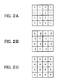
- FIG. 1A Assume that the input signal (8 bits) becomes as shown in FIG. 1A. To this, a 2 x 2 dither matrix of dither coefficients such as shown in FIG. 1B are added to the corresponding positions of the pixels. The results of the addition are shown in FIG. 1C. Since the input video signal is formed by 8 bits, the lower 2 bits are discarded (made 0) in order to enable the display of a display performance of 6 bits. The values when discarding the lower 2 bits are shown in FIG. 1D. For example, when an image data value after adding the dither coefficient in FIG.
- the higher 6 bits are advanced by 1 in the case where the dither coefficient is 3 or 2.
- the probability of the dither coefficient being 3 or 2 is 2/4, therefore the probability of the higher 6 bits being advanced by 1 is 2/4 in the case where the lower 2 bits are "2".
- the lower 2 bits among the original 8 bits of the input video signal are "3”
- the higher 6 bits are advanced by 1 in a case where the dither coefficient is 3, 2, or 1.
- the probability of the dither coefficient being 3, 2, or 1 is 3/4, therefore the probability of the higher 6 bits being advanced by 1 is 3/4 in the case where the lower 2 bits are "3".
- a difference ends up appearing in the image birefringence phase difference (retardation) in accordance with the viewing direction, so the colors of an image displayed on the display end up appearing changed.
- middle gray-scale display using a plurality of pixels can be realized by the above dither, the effect is exhibited only in a case where the display is viewed from a specific direction.
- a middle gray-scale cannot typically be precisely displayed when the image is viewed from any other directions. Namely, in a general liquid crystal display device etc., middle gray-scale expression can be realized, but there is the disadvantage that the viewing angle characteristic cannot be improved.
- An object of the present invention is to provide an image display device and method enabling a middle gray-scale display by using a plurality of pixels and simultaneously improving the viewing angle characteristic.
- a first aspect of the present invention is an image display device enabling a gray-scale display in accordance with an input video signal, having: a gray-scale converter for converting a gray-scale of an input video signal to characteristic values of pixels two-dimensionally arranged with respect to the image to be displayed, wherein the gray-scale converter converts a gray-scale so as to include, among the plurality of pixels expressing a middle gray-scale, at least one pixel converted to a first characteristic value obtained by adding a positive correction value to the gray-scale of the input video signal and at least one pixel converted to a second characteristic value obtained by adding a negative correction value.
- the device further has a correction value setter for setting the correction values in accordance with a middle gray-scale to be expressed.
- the gray-scale converter converts a gray-scale for a video signal expressed by primary color luminance components.
- the gray-scale converter converts a gray-scale so that either one of the first characteristic value or second characteristic value to which the positive or negative correction value has been added becomes a maximum characteristic value or a minimum characteristic value.
- a second aspect of the present invention is an image display device enabling a gray-scale display in accordance with an input video signal, having: a gray-scale expresser for expressing a middle gray-scale of the input video signal by a field train formed by a plurality of fields, wherein the gray-scale expresser expresses a gray-scale so as to include at least one field converted to a first characteristic value obtained by adding a positive correction value to the gray-scale of the input video signal and at least one field converted to a second characteristic value obtained by adding a negative correction value.
- the device further has a setter for setting the first characteristic value and the second characteristic value in accordance with a middle gray-scale to be displayed.
- the gray-scale expresser expresses by the field train a middle gray-scale of a video signal expressed by primary color luminance components.
- the gray-scale converter expresser expresses a gray-scale so that either one of the first characteristic value or second characteristic value becomes a maximum characteristic value or a minimum characteristic value.
- a third aspect of the present invention is an image display device enabling a gray-scale display in accordance with an input video signal, having: a gray-scale converter for converting a gray-scale of an input video signal to characteristic values of pixels two-dimensionally arranged with respect to the image to be displayed and a gray-scale expresser for expressing a middle gray-scale of the input video signal by a field train formed by a plurality of fields, wherein the gray-scale converter converts a gray-scale so as to include, among the plurality of pixels expressing a middle gray-scale, at least one pixel converted to a first characteristic value obtained by adding a positive correction value to the gray-scale of the input video signal and at least one pixel converted to a second characteristic value obtained by adding a negative correction value, and the gray-scale expresser expresses a gray-scale so as to include at least one field converted to a first characteristic value obtained by adding a positive correction value to the gray-scale of the input video signal and at least one field converted to a second characteristic value obtained by adding
- the device further has a controller for controlling the gray-scale converter to convert a gray-scale when the input video signal includes a moving picture and controlling the gray-scale expresser to express a middle gray-scale by a field train when the input video
- a fourth aspect of the present invention is an image display device enabling an expression of a middle gray-scale of an input video signal by a field train formed by a plurality of fields and a gray-scale display in accordance with an input video signal, having: a display including liquid crystal pixel cells displaying an image by a in accordance with in accordance with drive voltages and a drive portion for generating drive voltages corresponding to effective voltages including a first voltage corresponding to a bright level and a second voltage corresponding to a dark level, wherein the second voltage is set at a voltage lower than a threshold voltage of a liquid crystal cell.
- a fifth aspect of the present invention is an image display device enabling an expression of a middle gray-scale of an input video signal by a field train formed by a plurality of fields and a gray-scale display in accordance with an input video signal, having: a display including liquid crystal pixel cells displaying an image by a gray-scale in accordance with drive voltages and a drive portion for generating drive voltages corresponding to effective voltages including a first voltage corresponding to a bright level and a second voltage corresponding to a dark level, wherein the first voltage is set at a voltage higher than a voltage at which the characteristic value of a liquid crystal cell starts to become substantially the maximum.
- an optical thickness of each pixel cell is set in accordance with the first voltage value.
- a sixth aspect of the present invention is an image display device enabling an expression of a middle gray-scale of an input video signal by a field train formed by a plurality of fields and a gray-scale display in accordance with an input video signal, having: a display including liquid crystal pixel cells displaying an image by a gray-scale in accordance with drive voltages, wherein the display is driven while changing a bright/dark ratio over time.
- the display is driven so that the dark ratio in the bright/dark ratio becomes larger.
- the device further has a drive for generating drive voltages corresponding to effective voltages including a first voltage corresponding to a bright level and a second voltage corresponding to a dark level, and the first voltage is set at a voltage higher than the voltage at which the characteristic value of a liquid crystal cell starts to become substantially the maximum.
- a seventh aspect of the present invention is an image display method enabling a gray-scale display in accordance with an input video signal, having: a gray-scale conversion step of converting a gray-scale of an input video signal to characteristic values of pixels two-dimensionally arranged with respect to the image to be displayed, wherein the gray-scale conversion step converts a gray-scale so as to include, among the plurality of pixels expressing a middle gray-scale, at least one pixel converted to a first characteristic value obtained by adding a positive correction value to the gray-scale of the input video signal and at least one pixel converted to a second characteristic value obtained by adding a negative correction value.
- An eighth aspect of the present invention is an image display method enabling a gray-scale display in accordance with an input video signal, having: a gray-scale expression step of expressing a middle gray-scale of the input video signal by a field train formed by a plurality of fields, wherein the gray-scale expressing step expresses a gray-scale so as to include at least one field converted to a first characteristic value obtained by adding a positive correction value to the gray-scale of the input video signal and at least one field converted to a second characteristic value obtained by adding a negative correction value.
- a ninth aspect of the present invention is an image display method enabling a gray-scale display in accordance with an input video signal, having: a gray-scale conversion step of converting a gray-scale of an input video signal to characteristic values of pixels two-dimensionally arranged with respect to the image to be displayed and a gray-scale expression step of expressing a middle gray-scale of the input video signal by a field train formed by a plurality of fields, wherein the gray-scale conversion step converts a gray-scale so as to include, among the plurality of pixels expressing a middle gray-scale, at least one pixel converted to a first characteristic value obtained by adding a positive correction value to the gray-scale of the input video signal and at least one pixel converted to a second characteristic value obtained by adding a negative correction value, and the gray-scale expressing step expresses a gray-scale so as to include at least one field converted to a first characteristic value obtained by adding a positive correction value to the gray-scale of the input video signal and at least one field converted to a second characteristic value
- a 10th aspect of the present invention is an image display method enabling an expression of a middle gray-scale of an input video signal by a field train formed by a plurality of fields and a gray-scale display in accordance with an input video signal, having: a step of generating drive voltages corresponding to effective voltages including a first voltage corresponding to a bright level and a second voltage corresponding to a dark level and a step of applying the generated drive voltages to the liquid crystal cells, wherein the second voltage is set at a voltage lower than a threshold voltage of a liquid crystal cell.
- An 11th aspect of the present invention is an image display method enabling an expression of a middle gray-scale of an input video signal by a field train formed by a plurality of fields and a gray-scale display in accordance with an input video signal, having: a step of generating drive voltages corresponding to effective voltages including a first voltage corresponding to a bright level and a second voltage corresponding to a dark level and a step of applying the generated drive voltages to the liquid crystal cells, wherein the first voltage is set at a voltage higher than a voltage at which the characteristic value of the liquid crystal cell starts to become substantially the maximum.
- a 12th aspect of the present invention is an image display method enabling an expression of a middle gray-scale of an input video signal by a field train formed by a plurality of fields and a gray-scale display in accordance with an input video signal, having: driving a display including liquid crystal cells displaying an image by a gray-scale in accordance with drive voltages while changing a bright/dark ratio over time.
- the present invention it is possible to use a plurality of pixels to display a middle gray-scale and, at the same time, improve the viewing angle characteristic.
- FIG. 1A to FIG. 1D are diagrams for explaining general dither.
- FIG. 3 is a diagram showing an example of the configuration of an image display device according to a first embodiment of the present invention.
- the image display device 10 is provided with, as shown in FIG. 1, a luminance converter 11 for converting a video signal H given as an applied signal voltage to a luminance signal based on a predetermined nonlinear characteristic, an offset generator 12 supplied with the input video signal H, a first adder circuit 13 and a second adder circuit 14 for adding and subtracting output signals from the luminance converter 11 and an offset table, a first voltage converter 15 supplied with a computation result of the first adder circuit 13, a second voltage converter 16 supplied with a computation result of the second adder circuit 14, a ditherer 17 supplied with signals V1 and V2 output from the first and second voltage converters 15 and 16, a controller 18 for controlling the ditherer 17, and a display 19 for displaying an image in response to the input video signal H based on an output signal Cout from the ditherer 17.
- a luminance converter 11 for converting a video signal H given as an applied signal voltage to a luminance signal based on a predetermined nonlinear characteristic
- an offset generator 12 supplied
- the luminance converter 11 converts the supplied video signal H to a luminance signal L based on a previously set nonlinear characteristic.
- the nonlinear characteristic set in the luminance converter 11 can be freely set and may be expressed by for example a nonlinear curve having a gradient becoming more gentle as the voltage becomes lower.
- the signal L converted from voltage to luminance in the luminance converter 11 is supplied to the first adder circuit 13 and the second adder circuit 14.
- the offset generator 12 generates a signal D1 and a signal D2 expressed as pixel outputs correcting the gray-scale of the supplied video signal H (hereinafter, referred to as an input gray-scale).
- the offset generator 12 generates signals D1 and D2 for offsetting the luminance signal L from the luminance converter 11 with reference to a previously set offset table in accordance with the applied signal voltage of the supplied video signal H.
- the signal D1 generated at the offset generator 12 is output to the first adder circuit 13, and the signal D2 is output to the second adder circuit 14. Note that, details of the offset table in the offset generator 12 and the signals D1 and D2 to be generated will be explained later.
- the first adder circuit 13 is supplied with the signal L from the luminance converter 11 and supplied with the signal D1 from the offset generator 12. The first adder circuit 13 subtracts the signal D1 from the signal L and supplies a signal E1 obtained as a result to the first voltage converter 15.
- the second adder circuit 14 is supplied with the signal L from the luminance converter 11 and supplied with the signal D2 from the offset generator 12.
- the second adder circuit 14 adds the signal D2 to the signal L and supplies a signal E2 obtained as a result to the second voltage converter 16.
- the first voltage converter 15 converts the signal E1 supplied from the first adder circuit 13 to the ⁇ characteristic again based on the previously set nonlinear characteristic.
- This nonlinear characteristic set in the first voltage converter 15 is expressed as an inverse characteristic to the nonlinear characteristic set in the luminance converter 11. For this reason, when updating the nonlinear characteristic set in the luminance converter 11, the nonlinear characteristic set in the first voltage converter 15 will also be updated linked with this.
- the signal V1 converted by the first voltage converter 15 is output to the ditherer 17.
- the second voltage converter 16 converts the signal E2 supplied from the second adder circuit 14 to the ⁇ characteristic again based on the previously set nonlinear characteristic.
- This nonlinear characteristic set in the second voltage converter 16 is expressed as an inverse characteristic to the nonlinear characteristic set in the luminance converter 11. For this reason, when updating the nonlinear characteristic set in the luminance converter 11, the nonlinear characteristic set in the second voltage converter 16 will also be updated linked with this.
- the signal V2 converted by the second voltage converter 16 is output to the ditherer 17.
- the ditherer 17 performs dithering based on dither under the control of the controller 18 from the signals V1 and V2 supplied from the first voltage converter 15 and the second voltage converter 16.
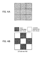
- FIGS. 4 are diagrams for explaining a case where the ditherer 17 of the present embodiment uses a dither matrix to perform the dithering.
- This dither as shown in FIG. 4A, pseudo expresses an image region expressed by a middle gray-scale comprised of a plurality of pixels by a two-dimensional dither matrix comprised of two types of pixels of pixels having a first characteristic value (transmittance in the present embodiment) and pixels having a second characteristic value (transmittance in the present embodiment) expressed by a checkerboard like regular pattern in the horizontal direction and the vertical direction as shown in FIG. 4B.
- the ditherer 17 outputs an output signal Cout expressed by such a dither matrix to the display 19.
- the display 19 for example displays the output image of the ditherer 17 via the direct view type liquid crystal display screen mounting thin film transistors (TFT) for driving liquid crystals
- TFT thin film transistors
- the display 19 obtains the predetermined transmittances (characteristic values) and displays the middle gray-scale by utilizing for example the liquid crystal material characteristic having a transmittance curve corresponding to the output signal Cout defined as the voltage value.
- FIG. 5 is a diagram showing the relationship of the pixel output to be corrected with respect to the input gray-scale.
- an abscissa indicates the input gray-scale (transmittance)
- an ordinate indicates the characteristic value (transmittance).
- predetermined dither coefficients are added to corresponding positions of a plurality of pixels.
- the input signal is corrected so that an average output obtained by addition by the plurality of pixels exhibits a linear relationship as shown by a straight line b in FIG. 5 with respect to the input gray-scale, whereby the resultant pixel output is obtained.
- a pair of pixels are corrected based on the relationships of pixel outputs shown by a and c in FIG. 5 with respect to the input gray-scale and controlled so as to obtain a first characteristic value VALa and a second characteristic value VALC.
- a plus correction value ⁇ k2 is added to the straight line b as shown in FIG. 5 to find the first characteristic value VALa, while a minus correction value ⁇ k1 is subtracted from the straight line b to find the second characteristic value VALC.
- the positive correction value ⁇ k2 and the negative correction value ⁇ k1 are generated with respect to the input gray-scale. These correction values are added to the input gray-scale to thereby obtain the pixel output b .
- the ditherer 17 is supplied with a signal V1 indicating the pixel output having the relationship of a with respect to the input gray-scale and a signal V2 indicating the pixel output having the relationship of c with respect to the input gray-scale.
- the ditherer 17 determines the first characteristic value VALa based on the signal V1, determines the second characteristic value VALc based on the signal V2, and expresses the middle gray-scale via the dither matrix.
- the middle gray-scale obtained by adding the first characteristic value VALa and the second characteristic value VALb and dividing the result by 2 is expressed by the dither matrix. This corresponds to the expression of the relationship obtained by adding pixel outputs (transmittances) expressed by the relationships of a and c shown in FIG. 5 and dividing the result by 2 via a dither matrix.
- the offset generator 12 stores in advance the relationships a and c of pixel outputs with respect to the input gray-scale in an offset table to refers to this offset table whenever the drive signal H is input so as to specify the correction values ⁇ k1 and ⁇ k2.
- the relationships a and c of the pixel outputs previously stored in the offset table are set to a format including at least one pixel converted to the first characteristic value VALa obtained by adding the negative correction value ⁇ k1 to the input gray-scale and at least one pixel converted to the second density obtained by adding the positive correction value ⁇ k2 to the input gray-scale in the dither matrix as shown in FIG. 5.
- the relationships a and c of the pixel outputs are stored in the offset table so that either of the first characteristic value or second characteristic value obtained as a result of adding the negative correction value ⁇ k1 and the positive correction value ⁇ k2 becomes the maximum characteristic value (transmittance: 100%) or the minimum characteristic value (transmittance: 0%).
- the negative correction value ⁇ k1 is set so that the second characteristic value becomes the minimum characteristic value from the transmittance 0% to 50%
- the positive correction value ⁇ k2 is set so that the first characteristic value becomes the maximum characteristic value from the transmittance 50% to 100%.
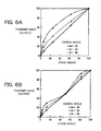
- FIG. 6A and FIG. 6B are diagrams showing the relationships of the transmittance with respect to viewing angles (0 degree, 20 degrees, 40 degrees, 60 degrees) with respect to the liquid crystal display screen of the display 19 in the case where the correction values are set as explained above, in which FIG. 6A shows the relationship of the transmittance with respect to the viewing angle in the case based on the usual dither, and FIG. 6B shows the relationship of the transmittance with respect to the viewing angle in the present embodiment.
- the abscissa indicates the transmittance (input) based on the output signal Cout supplied from the ditherer 17 in accordance with the gray-scale to be displayed in the display 19, and the ordinate indicates the transmittance (output) of the gray-scale actually displayed on the display 19.
- FIG. 7A and FIG. 7B are diagrams showing results expressing the relationships of transmittances shown in FIG. 6A and FIG. 6B by the ⁇ corrected gray-scale.
- the abscissas indicate input gray-scale
- the ordinates indicate output gray-scale.
- the dither matrix is formed so that the first characteristic value becomes the transmittance of 100% and the second characteristic value becomes the transmittance of 0% in the relationships a and c of pixel outputs.
- the viewing angle characteristic does not deteriorate when the transmittances are 0% and 100%, therefore a middle gray-scale of a dither matrix expressed by adding the first characteristic value and the second characteristic value and dividing the result by 2 does not deteriorate in the viewing angle characteristic when the transmittance is 50%. It is seen that deviation in accordance with the viewing angle does not occur in the case of a transmittance of 50% as shown in FIG. 6B.
- the viewing angle characteristic no longer deteriorates at least in regard to the second characteristic value. For this reason, when displaying a middle gray-scale of a dither matrix expressed by adding these first characteristic value and second characteristic value and dividing the result by 2, the viewing angle characteristic can be improved in comparison with the usual dither.
- the viewing angle characteristic no longer deteriorates at least in regard to the first characteristic value. For this reason, when displaying a middle gray-scale of a dither matrix expressed by adding these first characteristic value and second characteristic value and dividing the result by 2, the viewing angle characteristic can be improved in comparison with the usual dither.
- the present embodiment is not limited to the case where the relationships a and c of pixel outputs where either of the first characteristic value or second characteristic value becomes the maximum characteristic value or the minimum characteristic value are stored in the offset table. If at least one pixel converted to the first characteristic value (transmittance) obtained by adding the negative correction value ⁇ k1 to the input gray-scale and at least one pixel converted to the second characteristic value (transmittance) obtained by adding the positive correction value ⁇ k2 to the input gray-scale are included in the dither matrix, the same effect can be obtained. For example, curves where the relationships of pixel outputs shown in FIG. 5 are defined by a' and c' may be stored in the offset table as well.
- the present invention is not limited to such a case. Any format may be employed so far as the dither matrix is comprised of a plurality of pixels.
- the transmittance When the transmittance is 50% to 75%, the characteristic value of the pixel output of the pixel F3 is shifted to a large extent, while the pixels F1 and F2 are fixed at the maximum characteristic value and further the pixel F4 is fixed at the minimum characteristic value.
- the transmittance is 75% to 100%, the characteristic value of the pixel output of the pixel F4 is shifted to a large extent, while the pixels F1, F2, and F3 are fixed at the maximum characteristic value.
- the image display device 10 of the first embodiment when expressing a middle gray-scale of a dither matrix by a first characteristic value and a second characteristic value, only the characteristic value of one pixel composing this dither matrix is shifted.
- the characteristic values of the other pixels are typically fixed in characteristic values (transmittances) at 0% or 100%. Therefore it becomes possible to improve the viewing angle characteristic by that amount.
- an image processing apparatus 20 expressing a middle gray-scale of an input video signal by a field train comprised of a plurality of fields so as to improve the viewing angle characteristic will be explained.
- the image display device 10 of the first embodiment used the technique of dithering in the spatial direction to express one gray-scale by a plurality of pixels so as to improve the viewing angle characteristic.
- the image display device 20 of the second embodiment expresses one gray-scale by pixels of a plurality of screens arranged in the time direction to improve the viewing angle characteristic.
- one screen will be also referred to as a "field” and a train comprised of a plurality of fields will be referred to as a "field train”.
- field train a train comprised of a plurality of fields
- FIG. 9 is a block diagram showing an example of the configuration of the image display device 20 according to the second embodiment.
- the image display device 20 is provided with, as shown in FIG. 9, a nonlinear converter 21, an offset generator 22, an offset table 23, a first adder circuit 24, a second adder circuit 25, a first inverse converter 26, a second inverse converter 27, a time division processor 28, a controller 29 for controlling the time division processor 28, and a display 30.
- the nonlinear converter 21 receives as input a video signal H having a screen display rate of 60Hz from the outside.
- the nonlinear converter 21 converts the level of the input video signal H according to the predetermined nonlinear input/output characteristic set in advance.
- the nonlinear input/output characteristic set in the nonlinear converter 21 is a nonlinear curve expressed by a so-called gamma function where the gradient becomes gentler as the level becomes lower. Note that this nonlinear input/output characteristic can be freely set.
- the video signal L after the level conversion output from the nonlinear converter 21 is supplied to the first adder circuit 24 and the second adder circuit 25.
- the offset generator 22 receives as input the video signal H.
- the offset generator 22 refers to the offset table 23 and generates the first offset signal ⁇ k1 and the second offset signal ⁇ k2.
- the offset table 23 is a table showing values of corresponding offset signals ⁇ k1 and ⁇ k2 with respect to the signal level of the input video signal H.
- the offset generator 22 retrieves the corresponding ⁇ k1 and ⁇ k2 from the offset table in accordance with the input video signal H and outputs them as offset signals. Note that details for the first offset signal ⁇ k1 and the second offset signal ⁇ k2 output from the offset generator 22 will be explained later.
- the first offset signal ⁇ k1 output from the offset generator 22 is supplied to the first adder circuit 24.
- the second offset signal ⁇ k2 output from the offset generator 22 is supplied to the second adder circuit 25.
- the first adder circuit 24 receives as input the video signal L output from the nonlinear converter 21 and the first offset signal ⁇ k1 output from the offset generator 22.
- the first adder circuit 24 adds the video signal L and the first offset signal ⁇ k1 to generate a video signal E1.
- the video signal E1 generated by the first adder circuit 24 is supplied to the first inverse converter 26.
- the second adder circuit 25 receives as input the video signal L output from the nonlinear converter 21 and the second offset signal ⁇ k2 output from the offset generator 22.
- the second adder circuit 25 subtracts the first offset signal ⁇ k1 from the video signal L to generate a video signal E2.
- the video signal E2 generated by the second adder circuit 24 is supplied to the second inverse converter 27.
- the first inverse converter 26 receives as input the video signal E1 output from the first adder circuit 24.
- the first inverse converter 26 converts the level of the input video signal E1 according to the predetermined nonlinear input/output characteristic set in advance.
- the second inverse converter 27 receives as input the video signal E2 output from the second adder circuit 25.
- the second inverse converter 27 converts the level of the input video signal E2 according to the predetermined nonlinear input/output characteristic set in advance.
- the nonlinear input/output characteristics set in the first inverse converter 26 and the second inverse converter 27 are inverse characteristics to the nonlinear input/output characteristics set in the nonlinear converter 21. For example, if input/output characteristics in accordance with the gamma function are set in the nonlinear converter 21, this means that inverse gamma characteristics are set in the first inverse converter 26 and the second inverse converter 27. For this reason, when updating the nonlinear characteristics set in the nonlinear converter 21, the nonlinear characteristics set in the first inverse converter 26 and the second inverse converter 27 will also be updated linked with this.
- the video signal V1 after the level conversion by the first inverse converter 26 is supplied to the time division processor 28. Further, the video signal V2 after the level conversion by the second inverse converter 27 is supplied to the time division processor 28.
- the nonlinear converter 21 has the same components as those of the luminance converter 11 of the image display device 10 of the first embodiment
- the offset generator 22 and the offset table 23 have the same components as those of the offset generator 12 of the image display device 10 of the first embodiment
- the first adder circuit 24 has the same components as those of the first adder circuit 13 of the image display device 10 of the first embodiment
- the second adder circuit 25 has the same components as those of the second adder circuit 14 of the image display device 10 of the first embodiment.
- the first inverse converter 16 has the same components as those of the first voltage converter 15 of the image display device 10 of the first embodiment
- the second inverse converter 27 has the same components as those of the second voltage converter 26 of the image display device 10 of the first embodiment.
- the time division processor 28 has a first up convert unit 281, a second up convert unit 282, and a switch output unit 283.
- the first up convert unit 281 receives as input the video signal V1 after the level conversion by the first inverse converter 26.
- the video signal V1 has a screen display rate (60 Hz) the same as that of the original video signal H.
- the first up convert unit 281 converts the screen display rate of the input video signal V1 from 60 Hz to 120 Hz.
- the first up convert unit 281 performs the up conversion by repeatedly outputting for example the same screen two times.
- the second up convert unit 282 receives as input the video signal V2 after the level conversion by the second inverse converter 27.
- the video signal V2 has a screen display rate (60 Hz) the same as that of the original video signal H.
- the second up convert unit 282 converts the screen display rate of the input video signal V2 from 60 Hz to 120 Hz.
- the second up convert unit 282 performs the up conversion by repeatedly outputting for example the same screen two times.
- the switch output unit 283 alternately selects and outputs the video signal output from the first up convert unit 281 and the video signal output from the second up convert unit 282 for each screen.
- the switch output unit 283 outputs a video signal Cout having a screen display rate of 120 Hz in which a screen generated by the addition of the first offset signal ⁇ k1 and a screen generated by the addition of the second offset signal ⁇ k2 are alternately repeated.
- the video signal Cout output from the switch output unit 283 is supplied to the display 30.
- the display 30 displays the output image of the time division processor 28 via a direct view type liquid crystal display screen mounting for example thin film transistors (TFT) for driving the liquid crystals.
- TFT thin film transistors
- the liquid crystal display screen changes in the transmittance at the pixel positions corresponding to the video signal Cout to display different screens of the video signal.
- the alternating current of the liquid crystals is set at 60 Hz. This is so as to prevent the application of DC current to the liquid crystals and subsequent burn-in or flickering.
- the image display device 20 expresses one gray-scale by two consecutive screens arranged in the time direction so as to improve the viewing angle characteristic. Specifically, the following processing is carried out.
- the image display device 20 converts the screen display rate of the video signal from 60 Hz to 120 Hz.
- a preceding screen will be called the "first field”
- the following screen will be called the "second field”. Note that while the term “field” is used, this has no relation to the "field" of an interlaced scan.
- FIG. 10 is a diagram showing a characteristic value (transmittance of liquid crystal) displayed on the display 30 with respect to the signal level (gray-scale) of an input video signal H.
- the first offset signal ⁇ k1 is added to the first field FLD1, and the second offset signal ⁇ k2 is subtracted from the second field FLD2.
- an output video signal Cout in which a field corrected in level to the plus side (first field) and a field corrected in level to the minus side are alternately repeated is supplied to the display 30.
- the offset signals ⁇ k1 and ⁇ k2 are determined so that the video image becomes the same as the ordinary video image seen in the case where the offset signals ⁇ k1 and ⁇ k2 are not added when averaging the first field FLD1 and the second field FLD2.
- the offset generator 22 of the image display device 20 generates the first offset signal ⁇ k1 and the second offset signal ⁇ k2 by referring to the offset table 23.
- the offset table 23 stores in advance the relationship of the pixel output level with respect to the level of the original video signal (input gray-scale).
- the offset generator 22 specifies ⁇ k1 and ⁇ k2 by referring to the offset table 23 whenever a video signal H is input.
- the first field FLD1 becomes an image in which the entire screen is displayed by a gray-scale having the transmittance of 100%.
- the region of the upper half of the screen is displayed by a gray-scale having a transmittance of 0%
- the region of the lower half of the screen is displayed by a gray-scale having a transmittance of 100%.
- ⁇ k1 and ⁇ k2 are stored in the offset table 23 so that either of the resultant value obtained by adding the first offset signal ⁇ k1 or the resultant value by subtracting the second offset signal ⁇ k2 becomes the maximum characteristic value (transmittance of 100%) or the minimum characteristic value (transmittance of 0%).
- the maximum characteristic value transmittance of 100%
- the minimum characteristic value transmitmittance of 0%
- the second offset signal ⁇ k2 is set so that the characteristic value (transmittance) of the second field FLD2 becomes the minimum value (minimum transmittance) from the level of the input video signal of 0% to 50%
- the first offset signal ⁇ k1 is set so that the characteristic value (transmittance) of the first field FLD1 becomes the maximum value (maximum transmittance) from the level of the input video signal of 50% to 100%.
- the first field FLD1 of a time t0 to a time t1/2 is based on a transmittance gl
- the second field FLD2 of a time t1/2 to a time t1 is set at the transmittance 0%. Due to this, it becomes possible to pseudo project the middle gray-scale e1 for the image region to a user viewing the array of consecutive fields (hereinafter referred to as a "field train") from the time t0 to the time t1.
- the first field FLD1 of a time t0 to a time t1/2 is based on a transmittance g2, and the second field FLD2 of a time t1/2 to a time t1 is set at the transmittance 0%. Due to this, it becomes possible to pseudo project the middle gray-scale e2 for the image region to a user continuously viewing the field train from the time t0 to the time t1.
- the first field FLD1 of a time t0 to a time t1/2 is based on the transmittance 100%
- the second field FLD2 of a time t1/2 to a time t1 is set at a transmittance g3. Due to this, it becomes possible to pseudo project the middle gray-scale e3 for the image region to a user continuously viewing the field train from the time t0 to the time t1.
- Gray-scales may be displayed in any way so long as the gray-scales are expressed including at lease one field converted to a characteristic value obtained by adding a positive correction value (offset value) to the gray-scale of the video signal and at least one field converted to a characteristic value obtained by adding a negative correction value (offset value) to the gray-scale of the video signal in a field train comprised of two or more consecutive fields.
- the present invention is not limited to the first embodiment and the second embodiment explained above.
- the ditherer 17 may also be controlled to use the dither matrix as the two-dimensional image to express a middle gray-scale, while when the input video signal H is formed by a still image, it may be controlled to use a field train to express a middle gray-scale.
- the image display device may be provided with both of the configuration expressing a middle gray-scale by a dither matrix and the configuration expressing the same by a field train or may be provided with only one of the same.
- this image display device is not limited to the case where a middle gray-scale of a monochrome image is expressed.
- a middle gray-scale of a video signal expressed by the primary color luminance components of R, G, and B may be expressed based on the same technique as well.
- the correction values ⁇ k1 and ⁇ k2 set in the offset generator 12 may be freely set in advance by the user.
- this image display device 10 it is also possible to measure the so-called oblique viewing angle in the case where the liquid crystal display screen is obliquely viewed and optimize the dithering in the ditherer 17 based on the measured oblique viewing angle.
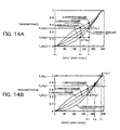
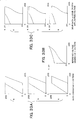
- FIG. 14A and FIG. 14B show transmittance characteristics with respect to the input gray-scale in cases where the viewing angle is 0 degree, 30 degrees, 45 degrees, and 60 degrees.
- the luminance obtained as a result of averaging T1(vl) and T2(v2) is defined as T0(v0) as shown in FIG. 14A.
- T1(vl) and T2(v2) is defined as T0(v0) as shown in FIG. 14A.
- ⁇ T(v1)/2+ ⁇ T(v2)/2 ⁇ T(v0) therefore ⁇ T60_dither becomes smaller than ⁇ T60_org, and the fluctuation of luminance depending on the viewing angle becomes small.
- the condition that the ⁇ T's be separate from each other in such a case until one side is clipped to 0 is most improved.
- the change of the gamma characteristic due to the oblique viewing angle becomes small.
- the found two values are utilized for spatial dither.
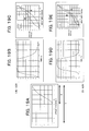
- the two values are found in accordance with the gamma characteristic for each pixel as explained above, and the point T(v1) brighter than the brightness of the original pixel and the point T(v2) darker than that between the two found values are displayed in a zigzag state as shown in FIG. 15A.
- FIG. 15B shows an example where a zigzag state of patterns found in FIG. 15A is reversed along with the elapse of time and these patterns are alternately displayed.
- any primary color luminance component may be replaced.
- FIG. 16A and FIG. 16B show an example where only G among R, G, and B is replaced.
- the two values of the luminance comprised of (r1,g2,b1) and the luminance comprised of (r2,g1,b2) are spatially arranged in a zigzag state. This arrangement is reversed by applying a time dither. In such case, not a zigzag arrangement of white and black, but an impression like a complementary color checkers' arrangement of G will be given to the user.
- the luminance difference between adjacent pixels is small, the mesh is hard to see, the edges are more smoothly seen, and the dither value is found for each pixel, therefore the deterioration of the resolution is small.
- FIG. 17 shows an example of installing a configuration optimizing the dithering based on the measured oblique viewing angle into the image display device 10.
- Pixels are arranged in a zigzag state as shown in FIG. 15A.
- the dither matrix is comprised of two values of a luminance comprised of (r1,g1,b1) and a luminance comprised of (r2,g2,b2)
- this means that the device is configured by a two-values generator 31 to which the video signal H comprised of the input luminance (r0,g0,b0) is input, an oblique viewing angle parameter portion 32 connected to this two-values generator 31, and a ditherer 17A.
- the two-values generator 31 finds the luminance (r1,g1,b1) and the luminance (r2,g2,b2) based on the above Equation (1) to Equation (4) with respect to the input video signal H.
- the two values of the luminances found in this two-values generator 31 are transmitted to the ditherer 17A.
- the two-values generator 31 refers to the oblique viewing angle parameter unit 32 managing the measured oblique viewing angles in the form of parameters when finding these two values of luminances.
- the ditherer 17A executes the dithering as explained above based on this.
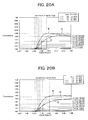
- the drive voltage is set within a range shown by for example X of FIG. 19A, that is, the black level is set at a value substantially the same as the threshold voltage, for example 1.9V, and the white level is set at 4.0V.
- the drive voltage waveform in this case is shown in FIG. 19B, and the transmittance characteristic with respect to the input gray-scale is shown in FIG. 19C.
- a sufficient sharpness is not obtained in rising and falling portions of the effective drive voltage waveform (sufficient response characteristic is not obtained).
- an actual characteristic shown by B tends to give a waveform different from an ideal curve shown by A.
- the drive voltage is set within the range shown by Y of FIG. 19A, that is, the black level is set at a voltage lower than the threshold voltage, for example 1.9V, i.e., 0V in the example of FIG. 19A, and the white level is set at 4.0V.
- the drive voltage waveform in this case is shown in FIG. 19D, and the transmittance characteristic with respect to the input gray-scale is shown in FIG. 19E.
- the voltage of the white level is set not a 4V exhibiting the maximum transmittance, but a value larger than 4V, for example 5V.
- the voltage of the white level is set not at 4V exhibiting the maximum transmittance, but a value larger than 4V, for example 5V.
- the optical cell thickness ⁇ nd of a pixel cell which was 310 nm with respect to a wavelength 546 nm (vicinity of wavelength of G) in the usual liquid crystal display device is set at 270 nm
- the optical cell thickness ⁇ nd of a pixel cell which was 330 nm with respect to a wavelength 450 nm (vicinity of wavelength of B) in the usual liquid crystal display device is set at 285 nm.
- the liquid crystal panel employing the second method is constituted so that the optical cell thickness becomes thin.
- the black level is set at a value in the vicinity of the threshold value in the same way as the usual liquid crystal display device or lower than the threshold value in the same way as the first method.
- FIG. 21A shows the transmittance characteristic with respect to the input gray-scale of a general liquid crystal display device corresponding to FIG. 20A
- FIG. 21B shows the transmittance characteristic with respect to an input gray-scale of a liquid crystal display device employing the second method of the present embodiment corresponding to FIG. 20B.
- the value of the white level of the drive voltage of the liquid crystal not at 4V at which the transmittance starts to become substantially the maximum, but at a voltage higher than 4V, for example 5V, and constituting the liquid crystal panel so that the optical thickness of the pixel cells becomes thin with respect to the predetermined wavelength corresponding to this, there is the advantage that improvement of the viewing angle characteristic of the middle gray-scale becomes possible.
- the drive voltage (application voltage) of the white level is made higher by 25% and the optical cell thickness is set thinner, i.e., about 86%, in comparison with the general display device, but the present invention is not limited to this.
- the present invention is not limited to this.
- Various aspects are possible.
- by further using a material having a low viscosity as the liquid crystal material a response speed of the liquid crystals becomes fast.
- the viewing angle characteristic can be improved.
- the third method basically employs a drive method giving a bright/dark ratio in time of 1:2.
- the lines in the vertical direction (V) are accessed not in line sequence, but alternately for bright and dark lines.
- a method of access where the dark data becomes 2 times the bright data is employed.
- a line #1 is accessed as the bright data
- a line #513 is accessed as the dark data next
- a line #2 is accessed as the bright data next
- a line #514 is accessed as the dark data next, this is sequentially repeated thereafter
- a line #256 is accessed as the bright data
- a line #768 (last line) is accessed as the dark data next
- a line #257 is accessed as the bright data next.
- Lines are generally accessed in the above sequence, then a line #1 is accessed as the dark data, a line #258 is accessed as the bright data next, the line #2 is accessed as the dark data next, and this is sequentially repeated thereafter.
- FIG. 23A shows the transmittance characteristic with respect to the input gray-scale of a general liquid crystal display device
- FIG. 23B shows the transmittance characteristic with respect to the input gray-scale of a liquid crystal display device employing the third method of the present embodiment.
- the actual characteristic shown by B tends to give a waveform different from the ideal curve shown by A.
- the actual characteristic shown by B tends to give a waveform approximating (approaching) the ideal curve shown by A.
- this ratio is not limited to 1:2.
- the explanation was given by taking as an example the first to third methods as the preferred method for driving a liquid crystal panel so that the bright/dark ratio in time becomes 1:2. It is also possible to employ these methods in combination. For example, it is also possible to employ a fourth method combining the second method (the method of setting the white level at 5V and making the optical cell thickness thin) and the third method (the method of changing the bright/dark ratio in time) or a fifth method combining so-called spatial sub pixels (an area ratio is for example 2:1) and the second method.
- FIG. 24A shows the transmittance characteristic with respect to the input gray-scale of a general liquid crystal device
- FIG. 24B shows the transmittance characteristic with respect to the input gray-scale of a liquid crystal display device employing the second method
- FIG. 24C shows the transmittance characteristic with respect to the input gray-scale of a liquid crystal display device employing the fourth method combining the second method and the third method.
- FIG. 25A shows the transmittance characteristic with respect to the input gray-scale of a liquid crystal display device corresponding to the general spatial sub pixel processing
- FIG. 25B shows the transmittance characteristic with respect to the input gray-scale of a liquid crystal display device employing the fifth method combining the second method of the present embodiment and spatial sub pixel processing.
- FIG. 26A shows voltage characteristic waveforms applied to a liquid crystal cell at bright and dark times with respect to the input of a general liquid crystal display device
- FIG. 26B shows voltage characteristic waveforms applied to a liquid crystal cell at bright and dark times with respect to the input of a liquid crystal display device employing the second method of the present embodiment
- FIG. 26C shows voltage characteristic waveforms applied to a liquid crystal cell at bright and dark times with respect to the input of a liquid crystal display device employing the fourth method combining the second method and the third method.
- a curve shown by VW shows the voltage waveform applied to the liquid crystal cell at the bright time
- a curve shown by VB shows the voltage waveform applied to the liquid crystal cell at the dark time.
- the range of expression of the black level becomes wide, so it is possible to effectively improve the viewing angle characteristic of the middle gray-scale.
- FIG. 27A shows voltage characteristic waveforms applied to a liquid crystal cell at bright and dark times with respect to the input of a general liquid crystal display device corresponding to the spatial sub pixel processing
- FIG. 27B shows voltage characteristic waveforms applied to a liquid crystal cell at bright and dark times with respect to the input of a liquid crystal display device employing the fifth method combining the second method of the present embodiment and spatial sub pixel processing.
- the curve shown by VW shows the voltage waveform applied to a liquid crystal cell at the bright time
- the curve shown by VB shows the voltage waveform applied to a liquid crystal cell at the dark time.
- the range of expression of the black level becomes wide, so it is possible to effectively improve the viewing angle characteristic of the middle gray-scale.
- bright application voltages VW and dark application voltages VB shown in FIG. 26A to FIG. 26C and FIGS. 27A and 27B are switched for each field and supplied to a so-called source driver at a stage in front of the liquid crystal panel.
- FIG. 28 is a diagram showing a first example of the configuration of a liquid crystal display device (image display device) which can be applied to the drive method of the present embodiment.
- This liquid crystal display device 40 has a data converter 41, a reference voltage generator 42, a source driver 43, and a display panel 44 as the display.
- the drive portion is configured by the data converter 41, the reference voltage generator 42, and the source driver 43.
- the drive method of the present embodiment can be applied.
- the data converter 41 has a ⁇ switch 410.
- the ⁇ switch 410 has a first field ⁇ characteristic holder 411, a second field ⁇ characteristic holder 412, and a ⁇ switching switch 413.
- the first field ⁇ characteristic holder 411 holds for example the characteristic voltage ⁇ pattern of the bright voltage VW set corresponding to the above ⁇ characteristic in a form of for example a LookUp Table.
- the second field ⁇ characteristic holder 412 holds for example the characteristic voltage ⁇ pattern of the dark voltage VB set corresponding to the above ⁇ characteristic in the form of for example a LookUp Table.
- the ⁇ switching switch 413 switches output data of the first field ⁇ characteristic holder 411 and the second field ⁇ characteristic holder 412 for each field and selectively outputs the same as the source driver signal to the source driver 43.
- the reference voltage generator 42 supplies a fixed reference voltage pattern to the source driver 43.
- the source driver 43 compares the source driver signal selectively supplied by the ⁇ switch 410 with the reference voltage pattern and outputs a predetermined drive signal to the display panel 44.
- FIG. 29 is a diagram showing a second example of the configuration of a liquid crystal display device which can be applied to the drive method of the present embodiment.
- This liquid crystal display device 40A has a reference voltage generator 42A, a source driver 43, and a display panel 44.
- the difference of the device 40A of FIG. 29 from the device of FIG. 28 resides in that the function of the ⁇ switch is imparted to the reference voltage generator 42A, and the original data is input to the source driver 43.
- the reference voltage generator 42A has a first field ⁇ characteristic holder 41, a second field ⁇ characteristic holder 422, and a ⁇ switch 423.
- the first field ⁇ characteristic holder 421 holds for example the characteristic voltage ⁇ pattern at the bright time set corresponding to the above ⁇ characteristic in the form of for example a LookUp Table.
- the second field ⁇ characteristic holder 422 holds for example the characteristic voltage ⁇ pattern at the dark time set corresponding to the above ⁇ characteristic in the form of for example a LookUp Table.
- the ⁇ switching switch 423 switches output data of the first field ⁇ characteristic holder 421 and the second field ⁇ characteristic holder 422 for each field and selectively outputs the same as the reference voltage to the source driver 43.
- the source driver 43 compares the supplied source driver signal with the reference voltage pattern and outputs a predetermined drive signal to the display panel 44.
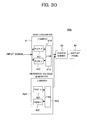
- FIG. 30 is a diagram showing a third example of the configuration of a liquid crystal display device which can be applied to the drive method of the present embodiment.
- This liquid crystal display device 40B has a configuration provided with the ⁇ switch 41 of FIG. 28 and the reference voltage generator 42A having the switch function of FIG. 29 together. Accordingly, the explanation of basic functions of the components will be omitted.
- FIG. 31A shows data conversion ⁇ patterns PVW and PVB held in the first field ⁇ characteristic holder 411 and the second field ⁇ characteristic holder 412 of the ⁇ switch 410
- FIG. 31B shows data conversion ⁇ patterns PVW and PVB held in the first field ⁇ characteristic holder 421 and the second field ⁇ characteristic holder 422 of the reference voltage generator 42A
- FIG. 31C shows the output (liquid crystal application voltage) characteristic of the source driver 43 with respect to the input data.
- the source driver 43 compares the ⁇ pattern selectively supplied from the ⁇ switch 410 for each field and the ⁇ pattern selectively supplied from the reference voltage generator 42A for each field to generate the bright voltage VW and dark voltage VB as shown in FIG. 31C and supplies the same to the display panel 44.
- FIG. 32 is a diagram showing a fourth example of the configuration of a liquid crystal display device which can be applied to the drive method of the present embodiment.
- this liquid crystal display device 40C from the device 40B of FIG. 30 resides in the configuration of performing ⁇ corrections of R, G, and B.
- the basic function of the ⁇ switch 410C of the data converter 41C is the same.
- the reference voltage generator 42A has the same configuration as that of the device 40B of FIG. 30. Accordingly, the explanation of basic functions of the components will be omitted.
- FIG. 33A shows data conversion ⁇ patterns PVW and PVB corresponding to R, G, and B held in a first field ⁇ characteristic holder 411C and a second field ⁇ characteristic holder 412C of a ⁇ switch 410C
- FIG. 33B shows data conversion ⁇ patterns PVW and PVB held in the first field ⁇ characteristic holder 421 and the second field ⁇ characteristic holder 422 of the reference voltage generator 42A
- FIG. 33C shows the output (liquid crystal application voltage) characteristics of the source driver 43 corresponding to R, G, and B with respect to the input data.
- the source driver 43 compares the ⁇ patterns corresponding to R, G, and B selectively supplied from the ⁇ switch 410C of the data converter 41C for each field and the ⁇ pattern selectively supplied from the reference voltage generator 42A for each field to generate the bright voltage VW and dark voltage VB as shown in FIG. 31C and supplies the same to the display panel 44.
- FIG. 34 is a diagram showing a fifth example of the configuration of a liquid crystal display device which can be applied to the drive method of the present embodiment.
- this liquid crystal display device 40D from the device 40B of FIG. 30 resides in the configuration corresponding to the sub pixel conversion processing, that is, the parallel arrangement of a sub pixel 1 system and a sub pixel 2 system with respect to the input signal.
- the functions of the components are the same as those in FIG. 30, so the explanation of the basic functions of the components will be omitted.
- FIG. 35A shows data conversion ⁇ patterns PVW1 and PVB1 held in the first field ⁇ characteristic holder 411 and the second field ⁇ characteristic holder 412 of a ⁇ switch 410-1
- FIG. 33B shows data conversion ⁇ patterns PVW2 and PVB2 held in the first field ⁇ characteristic holder 411 and the second field ⁇ characteristic holder 412 of a ⁇ switch 410-2
- FIG. 35C shows data conversion ⁇ patterns PVW1 and PVB1 held in the first field ⁇ characteristic holder 421 and the second field ⁇ characteristic holder 422 of a reference voltage generator 42A-1
- 35D shows data conversion ⁇ patterns PVW2 and PVB2 held in the first field ⁇ characteristic holder 421 and the second field ⁇ characteristic holder 422 of the reference voltage generator 42A-2
- FIG. 35E shows the output (liquid crystal application voltage) characteristic of the source driver 43 with respect to the input data.
- FIG. 36 is a diagram showing a sixth example of the configuration of a liquid crystal display device which can be applied to the drive method of the present embodiment.
- this liquid crystal display device 40E from the device 40D of FIG. 34 resides in the configuration for performing ⁇ corrections of R, G, and B.
- the rest of the configuration is the same as that of the device 40D. Accordingly, the explanation of basic functions of the components will be omitted.
- FIG. 37A shows the data conversion ⁇ patterns PVW1 and PVB1 held in the first field ⁇ characteristic holder 411 and the second field ⁇ characteristic holder 412 of the ⁇ switch 410-1
- FIG. 37B shows the data conversion ⁇ patterns PVW2 and PVB2 corresponding to R, G, and B held in the first field ⁇ characteristic holder 411 and the second field ⁇ characteristic holder 412 of the ⁇ switch 410-2
- FIG. 37C shows data conversion ⁇ patterns PVW1 and PVB1 held in the first field ⁇ characteristic holder 421 and the second field ⁇ characteristic holder 422 of the reference voltage generator 42A-1
- FIG. 37D shows data conversion ⁇ patterns PVW2 and PVB2 held in the first field ⁇ characteristic holder 421 and the second field ⁇ characteristic holder 422 of the reference voltage generator 42A-2
- FIG. 37E and FIG. 37F show the output (liquid crystal application voltage) characteristics corresponding to R, G, and B of the source driver 43 with respect to the input data.
- FIG. 38 is a diagram showing a seventh example of the configuration of a liquid crystal display device which can be applied to the drive method of the present embodiment.
- this liquid crystal display device 40F from the device 40D of FIG. 34 resides in that, in the ⁇ switch 410E of the data converter 41E, the first and second field ⁇ holders of the sub pixel 1 and the first and second field ⁇ holders of the sub pixel 2 are arranged in parallel and selectively switched by one ⁇ switch 413F to output the signal and in that the signal is corrected at the RGB ⁇ correction unit 414 and then output to the source driver 43. Accordingly, the device 40F of FIG. 38 can cope with sub pixel modulation processing by providing only one source driver 43 and reference voltage generator 42A.
- the present image display device and image display method can display a middle gray-scale by using a plurality of pixels and, at the same time, can improve the viewing angle characteristics, so can be applied to the direct view type liquid crystal display devices etc.
Landscapes
- Engineering & Computer Science (AREA)
- Physics & Mathematics (AREA)
- General Physics & Mathematics (AREA)
- Computer Hardware Design (AREA)
- Theoretical Computer Science (AREA)
- Chemical & Material Sciences (AREA)
- Crystallography & Structural Chemistry (AREA)
- Nonlinear Science (AREA)
- Mathematical Physics (AREA)
- Optics & Photonics (AREA)
- Control Of Indicators Other Than Cathode Ray Tubes (AREA)
- Liquid Crystal Display Device Control (AREA)
- Transforming Electric Information Into Light Information (AREA)
Applications Claiming Priority (3)
| Application Number | Priority Date | Filing Date | Title |
|---|---|---|---|
| JP2004210347 | 2004-07-16 | ||
| JP2005166014 | 2005-06-06 | ||
| PCT/JP2005/013144 WO2006009106A1 (ja) | 2004-07-16 | 2005-07-15 | 画像表示装置および画像表示方法 |
Publications (2)
| Publication Number | Publication Date |
|---|---|
| EP1662474A1 true EP1662474A1 (de) | 2006-05-31 |
| EP1662474A4 EP1662474A4 (de) | 2011-06-15 |
Family
ID=35785217
Family Applications (1)
| Application Number | Title | Priority Date | Filing Date |
|---|---|---|---|
| EP05766222A Withdrawn EP1662474A4 (de) | 2004-07-16 | 2005-07-15 | Vorrichtung und methode zur bildanzeige |
Country Status (6)
| Country | Link |
|---|---|
| US (1) | US20080272998A1 (de) |
| EP (1) | EP1662474A4 (de) |
| JP (1) | JP4882745B2 (de) |
| KR (1) | KR101115046B1 (de) |
| TW (1) | TW200617868A (de) |
| WO (1) | WO2006009106A1 (de) |
Cited By (4)
| Publication number | Priority date | Publication date | Assignee | Title |
|---|---|---|---|---|
| EP1884916A3 (de) * | 2006-08-02 | 2009-09-30 | Samsung Electronics Co., Ltd. | Ansteuerungsvorrichtung für eine Anzeigevorrichtung und Bildsignalausgleichsverfahren dafür |
| CN101174395B (zh) * | 2006-11-01 | 2010-09-29 | 索尼株式会社 | 液晶驱动器、液晶驱动方法和液晶显示设备 |
| US8159567B2 (en) | 2006-07-31 | 2012-04-17 | Sony Corporation | Image processing apparatus and image processing method |
| US9235067B2 (en) | 2006-06-02 | 2016-01-12 | Semiconductor Energy Laboratory Co., Ltd. | Display device and driving method thereof |
Families Citing this family (26)
| Publication number | Priority date | Publication date | Assignee | Title |
|---|---|---|---|---|
| JP2007212591A (ja) * | 2006-02-08 | 2007-08-23 | Hitachi Displays Ltd | 表示装置 |
| JP5048970B2 (ja) * | 2006-05-31 | 2012-10-17 | 株式会社ジャパンディスプレイイースト | 表示装置 |
| CN101647056B (zh) * | 2007-03-16 | 2013-01-23 | 索尼株式会社 | 图像处理设备、图像显示器和图像处理方法 |
| JP4525946B2 (ja) * | 2007-10-19 | 2010-08-18 | ソニー株式会社 | 画像処理装置、画像表示装置および画像処理方法 |
| EP2218306B1 (de) * | 2007-11-08 | 2016-10-12 | TP Vision Holding B.V. | Antriebspixel für eine anzeige |
| TWI374432B (en) | 2007-12-28 | 2012-10-11 | Novatek Microelectronics Corp | Image driving method and circuit for displaying apparatus and display apparatus |
| GB2457106A (en) * | 2008-03-04 | 2009-08-05 | Sharp Kk | LCD device with luminance variations perceivable only by off-axis viewers |
| JP4666016B2 (ja) | 2008-07-17 | 2011-04-06 | ソニー株式会社 | 表示装置およびその駆動方法ならびに電子機器 |
| US20110169880A1 (en) * | 2008-09-18 | 2011-07-14 | Tomoo Furukawa | Liquid crystal display device and method for driving liquid crystal display device |
| TWI407423B (zh) * | 2009-04-03 | 2013-09-01 | Himax Media Solutions Inc | 顯示資料處理裝置及顯示資料處理方法 |
| US9093031B2 (en) * | 2010-05-28 | 2015-07-28 | Sharp Laboratories Of America, Inc. | Off axis halo mitigation using spatiotemporal dither patterns, each indexed and arranged according to index patterns with diagonal lines of constant index |
| US20120081388A1 (en) * | 2010-09-30 | 2012-04-05 | Sharp Laboratories Of America, Inc. | Scaling for a lcd based upon viewing angle |
| WO2012147602A1 (ja) * | 2011-04-26 | 2012-11-01 | シャープ株式会社 | 液晶表示装置 |
| WO2013047300A1 (ja) * | 2011-09-27 | 2013-04-04 | シャープ株式会社 | 液晶表示装置およびその駆動方法 |
| EP2669882B1 (de) * | 2012-05-31 | 2019-10-09 | Samsung Display Co., Ltd. | Anzeigevorrichtung und Verfahren dafür |
| JP2014240926A (ja) * | 2013-06-12 | 2014-12-25 | パナソニック液晶ディスプレイ株式会社 | 液晶表示装置 |
| KR102185786B1 (ko) | 2014-02-27 | 2020-12-03 | 삼성디스플레이 주식회사 | 액정 표시 장치 및 및 액정 표시 장치의 구동 방법 |
| CN104157255B (zh) * | 2014-08-18 | 2016-08-17 | 深圳市华星光电技术有限公司 | 图像显示方法及显示系统 |
| KR102270258B1 (ko) * | 2014-11-28 | 2021-06-28 | 삼성디스플레이 주식회사 | 액정 표시 장치 및 그 구동방법 |
| US9947257B2 (en) * | 2015-07-24 | 2018-04-17 | Sharp Kabushiki Kaisha | Pixel layout and display with varying area and/or luminance capability of same type sub-pixels in different composite pixels |
| CN106470293B (zh) * | 2015-08-20 | 2019-07-09 | 联咏科技股份有限公司 | 图像处理装置及图像处理方法 |
| KR102637181B1 (ko) * | 2016-11-18 | 2024-02-15 | 삼성디스플레이 주식회사 | 표시 장치 및 그 구동 방법 |
| WO2019123632A1 (ja) * | 2017-12-22 | 2019-06-27 | Necディスプレイソリューションズ株式会社 | 映像処理装置、映像表示装置及び映像処理方法 |
| US12205509B2 (en) * | 2021-10-07 | 2025-01-21 | Novatek Microelectronics Corp. | Method for outputting grayscale data, driving controller and display apparatus |
| KR20230159736A (ko) * | 2022-05-12 | 2023-11-22 | 삼성디스플레이 주식회사 | 제어부, 이를 포함하는 표시 장치, 및 이를 이용한 표시 장치의 구동 방법 |
| CN116052570B (zh) * | 2022-12-26 | 2025-07-15 | 合肥大多数信息科技有限公司 | 一种多终端封装内核赋能方法 |
Family Cites Families (18)
| Publication number | Priority date | Publication date | Assignee | Title |
|---|---|---|---|---|
| JPS5498526A (en) * | 1978-01-20 | 1979-08-03 | Matsushita Electric Ind Co Ltd | Drive circuit of liquid crystal display unit |
| JPH0256522A (ja) * | 1988-08-23 | 1990-02-26 | Seiko Instr Inc | 液晶装置 |
| JPH03276968A (ja) * | 1989-09-19 | 1991-12-09 | Ikegami Tsushinki Co Ltd | 非線形量子化回路の誤差補正方法および回路 |
| JPH03251818A (ja) * | 1990-03-01 | 1991-11-11 | Matsushita Electric Ind Co Ltd | 液晶パネルの駆動方法および液晶制御回路 |
| JPH0568221A (ja) * | 1991-09-05 | 1993-03-19 | Toshiba Corp | 液晶表示装置の駆動方法 |
| JP3202450B2 (ja) * | 1993-10-20 | 2001-08-27 | 日本電気株式会社 | 液晶表示装置 |
| JPH07120724A (ja) * | 1993-10-28 | 1995-05-12 | Asahi Glass Co Ltd | 液晶ディスプレイ装置の中間調表示方法 |
| JPH07294881A (ja) * | 1994-04-20 | 1995-11-10 | Kodo Eizo Gijutsu Kenkyusho:Kk | 液晶表示装置 |
| JPH0990910A (ja) * | 1995-09-26 | 1997-04-04 | Matsushita Electric Ind Co Ltd | 液晶表示装置の駆動方法および液晶表示装置 |
| AUPP340998A0 (en) * | 1998-05-07 | 1998-05-28 | Canon Kabushiki Kaisha | A method of halftoning an image on a video display having limited characteristics |
| US6801220B2 (en) * | 2001-01-26 | 2004-10-05 | International Business Machines Corporation | Method and apparatus for adjusting subpixel intensity values based upon luminance characteristics of the subpixels for improved viewing angle characteristics of liquid crystal displays |
| KR100870487B1 (ko) * | 2001-07-04 | 2008-11-26 | 엘지디스플레이 주식회사 | 광시야각을 위한 액정디스플레이의 구동 방법 및 장치 |
| KR100769169B1 (ko) * | 2001-09-04 | 2007-10-23 | 엘지.필립스 엘시디 주식회사 | 액정표시장치의 구동방법 및 장치 |
| JP3627710B2 (ja) * | 2002-02-14 | 2005-03-09 | セイコーエプソン株式会社 | 表示駆動回路、表示パネル、表示装置及び表示駆動方法 |
| JP4079793B2 (ja) * | 2003-02-07 | 2008-04-23 | 三洋電機株式会社 | 表示方法、表示装置およびそれに利用可能なデータ書込回路 |
| JP4413515B2 (ja) * | 2003-03-31 | 2010-02-10 | シャープ株式会社 | 画像処理方法及びそれを用いた液晶表示装置 |
| CN100429692C (zh) * | 2003-10-16 | 2008-10-29 | 松下电器产业株式会社 | 矩阵型显示设备及其驱动方法 |
| JP4197322B2 (ja) * | 2004-01-21 | 2008-12-17 | シャープ株式会社 | 表示装置,液晶モニター,液晶テレビジョン受像機および表示方法 |
-
2005
- 2005-07-15 EP EP05766222A patent/EP1662474A4/de not_active Withdrawn
- 2005-07-15 TW TW094124189A patent/TW200617868A/zh not_active IP Right Cessation
- 2005-07-15 KR KR1020067005107A patent/KR101115046B1/ko not_active Expired - Fee Related
- 2005-07-15 US US10/571,911 patent/US20080272998A1/en not_active Abandoned
- 2005-07-15 WO PCT/JP2005/013144 patent/WO2006009106A1/ja not_active Ceased
- 2005-07-15 JP JP2006529180A patent/JP4882745B2/ja not_active Expired - Fee Related
Non-Patent Citations (2)
| Title |
|---|
| No further relevant documents disclosed * |
| See also references of WO2006009106A1 * |
Cited By (9)
| Publication number | Priority date | Publication date | Assignee | Title |
|---|---|---|---|---|
| US9235067B2 (en) | 2006-06-02 | 2016-01-12 | Semiconductor Energy Laboratory Co., Ltd. | Display device and driving method thereof |
| US10013923B2 (en) | 2006-06-02 | 2018-07-03 | Semiconductor Energy Laboratory Co., Ltd. | Display device and driving method thereof |
| US10714024B2 (en) | 2006-06-02 | 2020-07-14 | Semiconductor Energy Laboratory Co., Ltd. | Display device and driving method thereof |
| US11600236B2 (en) | 2006-06-02 | 2023-03-07 | Semiconductor Energy Laboratory Co., Ltd. | Display device and driving method thereof |
| US11657770B2 (en) | 2006-06-02 | 2023-05-23 | Semiconductor Energy Laboratory Co., Ltd. | Display device and driving method thereof |
| US8159567B2 (en) | 2006-07-31 | 2012-04-17 | Sony Corporation | Image processing apparatus and image processing method |
| EP1884916A3 (de) * | 2006-08-02 | 2009-09-30 | Samsung Electronics Co., Ltd. | Ansteuerungsvorrichtung für eine Anzeigevorrichtung und Bildsignalausgleichsverfahren dafür |
| US8294649B2 (en) | 2006-08-02 | 2012-10-23 | Samsung Electronics Co., Ltd. | Driving device for display device and image signal compensating method therefor |
| CN101174395B (zh) * | 2006-11-01 | 2010-09-29 | 索尼株式会社 | 液晶驱动器、液晶驱动方法和液晶显示设备 |
Also Published As
| Publication number | Publication date |
|---|---|
| TW200617868A (en) | 2006-06-01 |
| KR101115046B1 (ko) | 2012-03-13 |
| EP1662474A4 (de) | 2011-06-15 |
| TWI305340B (de) | 2009-01-11 |
| JPWO2006009106A1 (ja) | 2008-07-31 |
| US20080272998A1 (en) | 2008-11-06 |
| WO2006009106A1 (ja) | 2006-01-26 |
| JP4882745B2 (ja) | 2012-02-22 |
| KR20070031262A (ko) | 2007-03-19 |
Similar Documents
| Publication | Publication Date | Title |
|---|---|---|
| EP1662474A1 (de) | Vorrichtung und methode zur bildanzeige | |
| KR101256232B1 (ko) | 화상 표시 장치 및 화상 표시 방법 | |
| JP4768344B2 (ja) | 表示装置 | |
| JP5220268B2 (ja) | 表示装置 | |
| JP5793079B2 (ja) | 液晶ディスプレイの色ずれを低減する低減方法、装置およびコンピュータプログラム | |
| JP5863925B2 (ja) | 制御装置及び制御方法 | |
| KR100794412B1 (ko) | 화상 표시 장치 및 화상 표시 방법 | |
| US20120007900A1 (en) | Field-sequential color liquid crystal display and method for displaying colors thereof | |
| KR102510573B1 (ko) | 투명 표시 장치 및 그 구동 방법 | |
| CN101647056A (zh) | 图像处理设备、图像显示器和图像处理方法 | |
| US20110025726A1 (en) | Hold-type image display apparatus and display method using the hold-type image display apparatus | |
| US7319449B2 (en) | Image display apparatus and image display method | |
| JP2008268286A (ja) | 画像表示装置 | |
| JP5110788B2 (ja) | 表示装置 | |
| JP2011141557A (ja) | 表示装置 | |
| EP2109094A1 (de) | LCD-Umkehrungssteuerung | |
| CN100437736C (zh) | 图像显示设备和图像显示方法 | |
| KR102078995B1 (ko) | 화상 표시 장치 및 화상 표시 방법 | |
| US8044904B2 (en) | Display device | |
| JP2004334153A (ja) | 画像表示装置及び画像表示方法 | |
| KR101961231B1 (ko) | 화상 표시 장치 및 화상 표시 방법 | |
| JP2006235417A (ja) | 液晶表示装置 | |
| JP5068048B2 (ja) | 表示装置 | |
| KR101619048B1 (ko) | 액정 표시 장치의 구동 장치 및 구동 방법 |
Legal Events
| Date | Code | Title | Description |
|---|---|---|---|
| PUAI | Public reference made under article 153(3) epc to a published international application that has entered the european phase |
Free format text: ORIGINAL CODE: 0009012 |
|
| 17P | Request for examination filed |
Effective date: 20060312 |
|
| AK | Designated contracting states |
Kind code of ref document: A1 Designated state(s): DE FR GB |
|
| AX | Request for extension of the european patent |
Extension state: AL BA HR MK YU |
|
| RBV | Designated contracting states (corrected) |
Designated state(s): AT BE BG CH CY CZ DE DK EE ES FI FR GB GR HU IE IS IT LI LT LU LV MC NL PL PT RO |
|
| DAX | Request for extension of the european patent (deleted) | ||
| RBV | Designated contracting states (corrected) |
Designated state(s): DE FR GB |
|
| A4 | Supplementary search report drawn up and despatched |
Effective date: 20110517 |
|
| RIC1 | Information provided on ipc code assigned before grant |
Ipc: G09G 3/20 20060101ALI20110511BHEP Ipc: G09G 3/36 20060101AFI20060317BHEP |
|
| STAA | Information on the status of an ep patent application or granted ep patent |
Free format text: STATUS: THE APPLICATION HAS BEEN WITHDRAWN |
|
| 18W | Application withdrawn |
Effective date: 20130424 |