EP1662568A2 - Module de puissance, branche de phase et onduleur à trois phase - Google Patents
Module de puissance, branche de phase et onduleur à trois phase Download PDFInfo
- Publication number
- EP1662568A2 EP1662568A2 EP05257205A EP05257205A EP1662568A2 EP 1662568 A2 EP1662568 A2 EP 1662568A2 EP 05257205 A EP05257205 A EP 05257205A EP 05257205 A EP05257205 A EP 05257205A EP 1662568 A2 EP1662568 A2 EP 1662568A2
- Authority
- EP
- European Patent Office
- Prior art keywords
- layer
- electrically conductive
- power
- substrate
- modules
- Prior art date
- Legal status (The legal status is an assumption and is not a legal conclusion. Google has not performed a legal analysis and makes no representation as to the accuracy of the status listed.)
- Granted
Links
Images


Classifications
-
- H—ELECTRICITY
- H05—ELECTRIC TECHNIQUES NOT OTHERWISE PROVIDED FOR
- H05K—PRINTED CIRCUITS; CASINGS OR CONSTRUCTIONAL DETAILS OF ELECTRIC APPARATUS; MANUFACTURE OF ASSEMBLAGES OF ELECTRICAL COMPONENTS
- H05K1/00—Printed circuits
- H05K1/02—Details
- H05K1/14—Structural association of two or more printed circuits
- H05K1/147—Structural association of two or more printed circuits at least one of the printed circuits being bent or folded, e.g. by using a flexible printed circuit
-
- H—ELECTRICITY
- H10—SEMICONDUCTOR DEVICES; ELECTRIC SOLID-STATE DEVICES NOT OTHERWISE PROVIDED FOR
- H10W—GENERIC PACKAGES, INTERCONNECTIONS, CONNECTORS OR OTHER CONSTRUCTIONAL DETAILS OF DEVICES COVERED BY CLASS H10
- H10W40/00—Arrangements for thermal protection or thermal control
- H10W40/20—Arrangements for cooling
- H10W40/25—Arrangements for cooling characterised by their materials
- H10W40/255—Arrangements for cooling characterised by their materials having a laminate or multilayered structure, e.g. direct bond copper [DBC] ceramic substrates
-
- H—ELECTRICITY
- H10—SEMICONDUCTOR DEVICES; ELECTRIC SOLID-STATE DEVICES NOT OTHERWISE PROVIDED FOR
- H10W—GENERIC PACKAGES, INTERCONNECTIONS, CONNECTORS OR OTHER CONSTRUCTIONAL DETAILS OF DEVICES COVERED BY CLASS H10
- H10W90/00—Package configurations
-
- H—ELECTRICITY
- H05—ELECTRIC TECHNIQUES NOT OTHERWISE PROVIDED FOR
- H05K—PRINTED CIRCUITS; CASINGS OR CONSTRUCTIONAL DETAILS OF ELECTRIC APPARATUS; MANUFACTURE OF ASSEMBLAGES OF ELECTRICAL COMPONENTS
- H05K1/00—Printed circuits
- H05K1/02—Details
- H05K1/03—Use of materials for the substrate
- H05K1/0306—Inorganic insulating substrates, e.g. ceramic, glass
-
- H—ELECTRICITY
- H05—ELECTRIC TECHNIQUES NOT OTHERWISE PROVIDED FOR
- H05K—PRINTED CIRCUITS; CASINGS OR CONSTRUCTIONAL DETAILS OF ELECTRIC APPARATUS; MANUFACTURE OF ASSEMBLAGES OF ELECTRICAL COMPONENTS
- H05K2201/00—Indexing scheme relating to printed circuits covered by H05K1/00
- H05K2201/04—Assemblies of printed circuits
- H05K2201/044—Details of backplane or midplane for mounting orthogonal PCBs
-
- H—ELECTRICITY
- H05—ELECTRIC TECHNIQUES NOT OTHERWISE PROVIDED FOR
- H05K—PRINTED CIRCUITS; CASINGS OR CONSTRUCTIONAL DETAILS OF ELECTRIC APPARATUS; MANUFACTURE OF ASSEMBLAGES OF ELECTRICAL COMPONENTS
- H05K2201/00—Indexing scheme relating to printed circuits covered by H05K1/00
- H05K2201/07—Electric details
- H05K2201/0707—Shielding
- H05K2201/0715—Shielding provided by an outer layer of PCB
-
- H—ELECTRICITY
- H05—ELECTRIC TECHNIQUES NOT OTHERWISE PROVIDED FOR
- H05K—PRINTED CIRCUITS; CASINGS OR CONSTRUCTIONAL DETAILS OF ELECTRIC APPARATUS; MANUFACTURE OF ASSEMBLAGES OF ELECTRICAL COMPONENTS
- H05K2201/00—Indexing scheme relating to printed circuits covered by H05K1/00
- H05K2201/10—Details of components or other objects attached to or integrated in a printed circuit board
- H05K2201/10007—Types of components
- H05K2201/10189—Non-printed connector
-
- H—ELECTRICITY
- H05—ELECTRIC TECHNIQUES NOT OTHERWISE PROVIDED FOR
- H05K—PRINTED CIRCUITS; CASINGS OR CONSTRUCTIONAL DETAILS OF ELECTRIC APPARATUS; MANUFACTURE OF ASSEMBLAGES OF ELECTRICAL COMPONENTS
- H05K2201/00—Indexing scheme relating to printed circuits covered by H05K1/00
- H05K2201/10—Details of components or other objects attached to or integrated in a printed circuit board
- H05K2201/10227—Other objects, e.g. metallic pieces
- H05K2201/10287—Metal wires as connectors or conductors
-
- H—ELECTRICITY
- H05—ELECTRIC TECHNIQUES NOT OTHERWISE PROVIDED FOR
- H05K—PRINTED CIRCUITS; CASINGS OR CONSTRUCTIONAL DETAILS OF ELECTRIC APPARATUS; MANUFACTURE OF ASSEMBLAGES OF ELECTRICAL COMPONENTS
- H05K3/00—Apparatus or processes for manufacturing printed circuits
- H05K3/0058—Laminating printed circuit boards onto other substrates, e.g. metallic substrates
- H05K3/0061—Laminating printed circuit boards onto other substrates, e.g. metallic substrates onto a metallic substrate, e.g. a heat sink
-
- H—ELECTRICITY
- H05—ELECTRIC TECHNIQUES NOT OTHERWISE PROVIDED FOR
- H05K—PRINTED CIRCUITS; CASINGS OR CONSTRUCTIONAL DETAILS OF ELECTRIC APPARATUS; MANUFACTURE OF ASSEMBLAGES OF ELECTRICAL COMPONENTS
- H05K3/00—Apparatus or processes for manufacturing printed circuits
- H05K3/36—Assembling printed circuits with other printed circuits
- H05K3/361—Assembling flexible printed circuits with other printed circuits
-
- H—ELECTRICITY
- H10—SEMICONDUCTOR DEVICES; ELECTRIC SOLID-STATE DEVICES NOT OTHERWISE PROVIDED FOR
- H10W—GENERIC PACKAGES, INTERCONNECTIONS, CONNECTORS OR OTHER CONSTRUCTIONAL DETAILS OF DEVICES COVERED BY CLASS H10
- H10W72/00—Interconnections or connectors in packages
- H10W72/071—Connecting or disconnecting
- H10W72/075—Connecting or disconnecting of bond wires
- H10W72/07551—Connecting or disconnecting of bond wires characterised by changes in properties of the bond wires during the connecting
- H10W72/07554—Connecting or disconnecting of bond wires characterised by changes in properties of the bond wires during the connecting changes in dispositions
-
- H—ELECTRICITY
- H10—SEMICONDUCTOR DEVICES; ELECTRIC SOLID-STATE DEVICES NOT OTHERWISE PROVIDED FOR
- H10W—GENERIC PACKAGES, INTERCONNECTIONS, CONNECTORS OR OTHER CONSTRUCTIONAL DETAILS OF DEVICES COVERED BY CLASS H10
- H10W72/00—Interconnections or connectors in packages
- H10W72/50—Bond wires
- H10W72/531—Shapes of wire connectors
- H10W72/533—Cross-sectional shape
- H10W72/534—Cross-sectional shape being rectangular
-
- H—ELECTRICITY
- H10—SEMICONDUCTOR DEVICES; ELECTRIC SOLID-STATE DEVICES NOT OTHERWISE PROVIDED FOR
- H10W—GENERIC PACKAGES, INTERCONNECTIONS, CONNECTORS OR OTHER CONSTRUCTIONAL DETAILS OF DEVICES COVERED BY CLASS H10
- H10W72/00—Interconnections or connectors in packages
- H10W72/50—Bond wires
- H10W72/531—Shapes of wire connectors
- H10W72/5363—Shapes of wire connectors the connected ends being wedge-shaped
-
- H—ELECTRICITY
- H10—SEMICONDUCTOR DEVICES; ELECTRIC SOLID-STATE DEVICES NOT OTHERWISE PROVIDED FOR
- H10W—GENERIC PACKAGES, INTERCONNECTIONS, CONNECTORS OR OTHER CONSTRUCTIONAL DETAILS OF DEVICES COVERED BY CLASS H10
- H10W72/00—Interconnections or connectors in packages
- H10W72/50—Bond wires
- H10W72/541—Dispositions of bond wires
- H10W72/5445—Dispositions of bond wires being orthogonal to a side surface of the chip, e.g. parallel arrangements
-
- H—ELECTRICITY
- H10—SEMICONDUCTOR DEVICES; ELECTRIC SOLID-STATE DEVICES NOT OTHERWISE PROVIDED FOR
- H10W—GENERIC PACKAGES, INTERCONNECTIONS, CONNECTORS OR OTHER CONSTRUCTIONAL DETAILS OF DEVICES COVERED BY CLASS H10
- H10W72/00—Interconnections or connectors in packages
- H10W72/50—Bond wires
- H10W72/541—Dispositions of bond wires
- H10W72/547—Dispositions of multiple bond wires
- H10W72/5473—Dispositions of multiple bond wires multiple bond wires connected to a common bond pad
-
- H—ELECTRICITY
- H10—SEMICONDUCTOR DEVICES; ELECTRIC SOLID-STATE DEVICES NOT OTHERWISE PROVIDED FOR
- H10W—GENERIC PACKAGES, INTERCONNECTIONS, CONNECTORS OR OTHER CONSTRUCTIONAL DETAILS OF DEVICES COVERED BY CLASS H10
- H10W72/00—Interconnections or connectors in packages
- H10W72/50—Bond wires
- H10W72/541—Dispositions of bond wires
- H10W72/547—Dispositions of multiple bond wires
- H10W72/5475—Dispositions of multiple bond wires multiple bond wires connected to common bond pads at both ends of the wires
-
- H—ELECTRICITY
- H10—SEMICONDUCTOR DEVICES; ELECTRIC SOLID-STATE DEVICES NOT OTHERWISE PROVIDED FOR
- H10W—GENERIC PACKAGES, INTERCONNECTIONS, CONNECTORS OR OTHER CONSTRUCTIONAL DETAILS OF DEVICES COVERED BY CLASS H10
- H10W72/00—Interconnections or connectors in packages
- H10W72/50—Bond wires
- H10W72/551—Materials of bond wires
- H10W72/552—Materials of bond wires comprising metals or metalloids, e.g. silver
- H10W72/5524—Materials of bond wires comprising metals or metalloids, e.g. silver comprising aluminium [Al]
-
- H—ELECTRICITY
- H10—SEMICONDUCTOR DEVICES; ELECTRIC SOLID-STATE DEVICES NOT OTHERWISE PROVIDED FOR
- H10W—GENERIC PACKAGES, INTERCONNECTIONS, CONNECTORS OR OTHER CONSTRUCTIONAL DETAILS OF DEVICES COVERED BY CLASS H10
- H10W72/00—Interconnections or connectors in packages
- H10W72/851—Dispositions of multiple connectors or interconnections
- H10W72/874—On different surfaces
- H10W72/884—Die-attach connectors and bond wires
-
- H—ELECTRICITY
- H10—SEMICONDUCTOR DEVICES; ELECTRIC SOLID-STATE DEVICES NOT OTHERWISE PROVIDED FOR
- H10W—GENERIC PACKAGES, INTERCONNECTIONS, CONNECTORS OR OTHER CONSTRUCTIONAL DETAILS OF DEVICES COVERED BY CLASS H10
- H10W90/00—Package configurations
- H10W90/701—Package configurations characterised by the relative positions of pads or connectors relative to package parts
- H10W90/751—Package configurations characterised by the relative positions of pads or connectors relative to package parts of bond wires
- H10W90/753—Package configurations characterised by the relative positions of pads or connectors relative to package parts of bond wires between laterally-adjacent chips
Definitions
- the invention relates generally to power modules and, more particularly, to low inductance power modules for high power electronic applications.
- Modern power semiconductor switches such as silicon Insulated Gate Bipolar Transistors (IGBTs) are capable of switching at much higher frequencies than earlier designs. Their lower switching losses enable new applications requiring high frequency power conversion.
- IGBTs Insulated Gate Bipolar Transistors
- problems associated with the high parasitic inductance of conventional packaging technologies In particular, the voltage overshoot that occurs when a power device is switched off is proportional to the product of the parasitic inductance and the slope of the IGBT current during the switching. Because of the faster switching transitions of the new IGBTs, reducing the parasitic inductance is more critical for the new generation of power devices, to avoid excessive voltage overshoots when switching the devices off. For example, a converter operating at 500V DC bus with a 50nH parasitic inductance and a relatively fast switching transition of 5A/ns would lead to a 50% voltage overshoot.
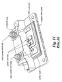
- FIG. 11 A conventional power module with screw type power terminals is shown in FIG. 11.
- the parasitic inductance of conventional power modules is approximately 20 nH and the phase-leg inductance of conventional designs is typically in excess of 50 nH.
- the screw type power terminal leads contribute a large share of the parasitic inductance, with the remainder contributed by wire bonds and the layout of the substrates. In addition to their high parasitic inductance, the non-symmetric layouts result in poor current sharing between power devices. Accordingly, the use of conventional power modules with the new generation of fast IGBT devices undesirably leads to significantly higher electrical stresses.
- Mourick et al. "750 A, 75 V MOSFET Power Module with Sub-nH Inductance," September 2, 2002, IEEE, Proceedings of the 14 th International Symposium on Power Semiconductor Devices and ICs, describe a low inductance multi-chip interconnect featuring a number of conductive webs that enable three-dimensional interleaving with power devices. During each switching transition, opposing magnetic fields are created by the currents through the power devices and by the currents in the conductive webs. The opposing magnetic fields cancel, resulting in a 2 nH parasitic inductance for the interconnect.
- Mourick et al. fail to address the design of a low parasitic inductance interconnect at the module and converter level.
- Other shortcomings of this design include the increased cost due to the addition of conductive webs, as well as the overall complexity of the module assembly.
- Arai et al. feature a pair of conventional power terminals that keep the module inductance high.
- the layout is not symmetrical, which can lead to problems with dynamic and static current sharing between parallel power device die.
- a power module includes at least one substrate that includes an upper layer, an electrical insulator and a thermal coupling layer.
- the upper layer includes at least one electrically conductive pattern and is configured for receiving at least one power device.
- the electrical insulator is disposed between the upper layer and the thermal coupling layer.
- the thermal coupling layer is configured for thermal conduction to a heat sink.
- the power module further includes at least one laminar interconnect that includes a first electrically conductive layer, an insulating layer and a second electrically conductive layer.
- the insulating layer is disposed between the first and second electrically conductive layers, and the first electrically conductive layer of the laminar interconnect is electrically connected to the upper layer of the substrate. Electrical connections connect a top side of the at least one power device to the second electrically conductive layer of the laminar interconnect.
- a power module assembly in accordance with another embodiment of the present invention, includes a number of power modules, a number of receptacles configured to receive the laminar interconnects of respective ones of the power modules, and a back plane.
- the back plane includes a positive direct current (DC) power bus layer, an output layer, and a negative DC power bus layer.
- the receptacles are mounted on the back plane.
- a modular phase leg assembly in accordance with another embodiment of the invention, includes two power modules, and each of the power modules includes a heat sink, a substrate attached to the heat sink, and at least one switch that includes at least one transistor and at least one anti-parallel diode and is mounted on the electrically conductive pattern of the upper layer of the substrate.
- Each of the power modules further includes a housing, encasing the substrate and at least one switch, and a laminar interconnect.
- the first electrically conductive layer of the laminar interconnect is electrically connected to the upper layer of the substrate. Electrical connections connect an anode of the at least one anti-parallel diode to the second electrically conductive layer of the laminar interconnect.
- a modular three-phase inverter assembly in accordance with another embodiment of the invention, includes six power modules, a number of receptacles configured to receive the laminar interconnects of respective ones of the power modules, and a back plane.
- the receptacles are mounted on the back plane.
- the power modules are arranged in three pairs, and each of the pairs corresponds to a phase leg.
- power module 10 includes a substrate 12 with an upper layer 16 that includes at least one electrically conductive pattern 17 and is configured for receiving at least one power device 14.
- An exemplary electrically conductive pattern 17 is illustrated in FIG. 1.
- substrate 12 further includes an electrical insulator 26 and a thermal coupling layer 28. Electrical insulator 26 is disposed between upper layer 16 and thermal coupling layer 28. Thermal coupling layer 28 is configured for thermal coupling to a heat sink 30.
- Power module 10 further includes a laminar interconnect 18 that includes a first electrically conductive layer 20, an insulating layer 22 and a second electrically conductive layer 24, as shown for example in FIG. 1.
- the insulating layer 22 is disposed between first and second electrically conductive layers 20, 24.
- First electrically conductive layer 20 of laminar interconnect 18 is electrically connected to upper layer 16 of substrate 12.
- electrical connections 42 connect a top side 19 of the power devices 14 to the second electrically conductive layer 24 of laminar interconnect 18.
- the electrical connections are wire bonds 42.
- the contribution of the interconnect to the overall parasitic inductance is reduced.
- upper layer 16 includes a number of connected and/or disconnected conductive regions that form electrically conductive pattern 17 and are arranged in the same plane. Upper layer 16 is electrically conductive.
- the phrase "electrically connected to” encompasses connecting two elements by wiring, solder, power overlay, bonding, or other electrical connection means.
- upper layer 16 of substrate 12 is soldered to first conductive layer 20 of laminar interconnect 18.
- the bottom side (not shown) of all power devices 14, such as the IGBT collector (or MOSFET drain) and diode cathode, are interconnected.
- substrate 12 is formed of direct bonded copper (DBC) or an active metal braze (AMB) structure. Both DBC and AMB refer to a process for directly bonding copper layers to a ceramic substrate. Exemplary DBC or AMB substrates are formed of copper-ceramic-copper layers. DBC and AMB provide a convenient structure for substrate 12, and the use of the same conductive material (in this case, copper) on both sides of electrical insulator 26 provides thermal and mechanical stability.
- DBC direct bonded copper
- AMB active metal braze
- electrical insulator 26 is thermally conductive.
- Exemplary electrical insulators include aluminum-oxide (AL 2 O 3 ), aluminum nitride (AIN), Beryllium Oxide (BeO) and silicon nitride (Si 3 N 4 ), which are thermally conductive.
- Exemplary insulating layers 22 include FR4, Kapton, other insulating polymers, and other insulating materials. According to a particular embodiment (not shown), insulating layer 22 extends beyond first and second conductive layers 20, 24 by a creepage distance to avoid electrical breakdown at the edge of laminar interconnect 18. As is known to those skilled in the art, a general rule for determining the creepage distance is 100 mils per Kilovolt, where a mil is one-thousandth of an inch. Exemplary conductive layers are formed of copper. Gold-bonded copper is also used to reduce oxidation.
- Cooling is a design concern for power electronics. Many cooling techniques can be employed for power module 10, including flat-surface cooling techniques, examples of which include liquid cooling, micro-channel cooling, and conventional heat sinks.
- thermal coupling layer 28 is configured for coupling to a base plate 30.
- thermal coupling layer 28 may be soldered or otherwise bonded to base plate 30.
- a DBC or AMB substrate 12 can be bonded to base plate 30 using any one of a number of techniques, including brazing, bonding, diffusion bonding, soldering, or pressure contact such as clamping. This provides a simple assembly process.
- power module 10 includes a heat sink 30, which comprises base plate 30. As shown, substrate 12 is attached to base plate 30.
- heat sink 30 includes a number of micro-channels (not shown in this application).
- the micro-channels are formed in conductive (for example, copper) layer 28 disposed between insulator 26 and base plate 30.
- the micro-channels are formed in a ceramic insulator 26 which is disposed between upper layer 16 and either an optional conductive layer or base plate 30.
- heat sink 30 conducts heat away from power devices 14, in order to accommodate high power densities.
- power module 10 further includes a number of power devices 14 mounted on substrate 12, the power devices being electrically connected to upper layer 16 of substrate 12.
- Exemplary power devices include transistors, such as Insulated Gate Bipolar Transistors (IGBT), Metal Oxide Semiconductor Field Effect Transistors (MOSFET), Metal Semiconductor Field Effect Transistors (MESFET), and High Electron Mobility Transistors (HEMT), and diodes.
- IGBT Insulated Gate Bipolar Transistors
- MOSFET Metal Oxide Semiconductor Field Effect Transistors
- MESFET Metal Semiconductor Field Effect Transistors
- HEMT High Electron Mobility Transistors
- electrical connections 42, 43 connect a top side 19 of power devices 14 to second electrically conductive layer 24 of laminar interconnect 18.
- the power devices 14 may be mounted on substrate 12 via a solder layer 15, as indicated in FIG. 3.
- the IGBT emitter or MOSFET source
- diode anode are interconnected.
- the parasitic inductance is reduced.
- the electrical connections are wire bonds 42.
- Exemplary wire bonds include 10-15 mil aluminum wire bonds. Ribbon bonds are another type of electrical connection.
- FIG. 2 illustrates another embodiment for which the electrical connections comprise at least one power overlay 43, which overlays the top-sides (not shown in FIG. 2) of the power devices 14.
- Power overlays are described in commonly assigned U.S. Patent No. 6,377,461, Ozmat et al, entitled "Power electronic module packaging.”
- Power overlays typically include at least one conductive and insulating layer and a number of vias (metal plugs). Exemplary insulating layers are formed of Kapton. Beneficially, power overlays are more robust than wire bonds and reduce the parasitic resistance and inductance relative to wire bonds.
- electrical connections 17 and 42 or 43 are symmetric for static (steady-state) and dynamic (transient) current sharing.
- symmetric it is meant that the total length of the respective electrical connections between the power devices 14 and the first and second conductive layers 20 and 24 is substantially the same.
- conventional power module designs provide current paths of varying lengths between power devices and the power terminals. Consequently, devices with shorter current paths are subject to greater stresses than are those power devices with longer current paths.
- FIGS. 1 and 2 provide excellent static and dynamic current sharing between parallel power devices 14.
- the power devices 14 include at least one transistor 36 and/or at least one anti-parallel diode 38 forming at least one switch 34.
- switch 34 is a 400A switch and includes four (4) transistors and four (4) anti-parallel diodes. This configuration is merely exemplary, and switch 34 may have other current ratings and correspondingly, other transistor/anti-parallel diode configurations, depending on the desired application for switch 34.
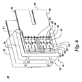
- Switch 34 is mounted on electrically conductive pattern 17, as indicated in FIG. 6.
- the electrical connections are shown as wire bonds 42 in FIG. 6 and connect the anodes of diodes 38 to the second electrically conductive layer 24 of laminar interconnect 18.
- the electrical connections may also take the form of ribbon bonds or one or more power overlays 43, as discussed above with respect to FIG. 2.
- Exemplary transistors include insulated gate bipolar transistors (IGBTs), which have emitters and collectors, and MOSFETs, which have sources and drains.
- IGBTs insulated gate bipolar transistors
- MOSFETs MOSFETs
- the electrical connections which are shown in FIG. 6 as wire bonds 42, connect the IGBT emitters to the anodes of respective anti-parallel diodes 38.
- MOSFETs with internal anti-parallel body diodes, the electrical connections connect MOSFET sources to the second electrically conductive layer 24.
- MOSFETs with external high performance diodes, e.g., Schottky diode.
- the electrical connections connect MOSFET sources to the anode of the respective anti-parallel diodes.
- power module 10 includes a number of transistors 36, with at least one of the transistors being a MOSFET and at least another of the transistors being an IGBT. More generally, power module 10 includes at least two different types of transistors 36. Similarly, for another embodiment, power module 10 includes at least two types of diodes 38. For example, power module 10 includes a number of anti-parallel diodes, with at least one of the diodes being a bipolar diode and at least another of the diodes being a Schottky diode.
- switch 34 includes at least two transistors 36 and at least two anti-parallel diodes 38.
- switch 34 has four transistors 36 and 4 anti-parallel diodes 38 and is configured as a 400A switch, for example.
- upper layer 16 of substrate 12 includes electrically conductive pattern 17, and switch 34 is disposed on pattern 17.
- Switch 34 further includes gate and return leads 63 formed on pattern 17. Electrical connections, shown in FIG. 6 as gate wire bonds 64, symmetrically connect each of the transistors 36 to the gate leads 63, which further improves static and dynamic current sharing between the power devices 14.
- laminar interconnect 18 is an edge card connector 18 configured for connecting to a receptacle 44 mounted on a back plane 46.
- exemplary receptacles are shown in FIG. 4, while FIG. 5 shows two receptacles 44 mounted on back plane 46.
- Receptacles 44 have interior contact surfaces 54 for making contact with edge card connector 18 and exterior contact surface 56 for making contact with back plane 46.
- the contact surfaces may be smooth or scored, and exemplary contact surfaces are formed using copper or gold-plated copper.
- back plane 46 includes a positive direct current DC bus layer 48, an output layer 50, and a negative DC bus layer 52.
- the interconnect inductance is reduced relative to conventional power modules.
- the power module 10 further includes a housing 32 encasing substrate 12, according to a particular embodiment.
- FIG. 7 shows an exemplary housing 32.
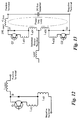
- FIG. 12 is an equivalent circuit diagram for the single switch power module.
- L IGBT is the package inductance when the IGBT is conducting
- L Diode is the package inductance when the anti-parallel diode is conducting.
- L conn is the contribution to the package inductance of the laminar interconnect that is shared between the IGBT and the anti-parallel diode.
- L sQ is the contribution to the package inductance associated with at least one wire bond 42 and the portion of electrically conductive pattern 17 between the IGBT die and the anti-parallel diode die.
- L sD is the contribution to the package inductance associated with at least one wire bond 42 and the portion of electrically conductive pattern 17 between the diode die and the laminar interconnect. In the example, the following parameter values were employed.
- the conductor width on the module was set to 51 mm, and the conductor width on the connector was selected to be 86 mm.
- a conductor spacing of 2.5 mm on the electrically conductive pattern 17 was used, and the spacing of the two conductive layers 16, 28 on the connector of 0.635 mm was selected.
- the heat-sink width and thickness were set to 51 mm and 5 mm, respectively.
- the simulation results included: a total switch module inductance of 0.93 nH, a gate inductance of 9.2 nH at 1 MHz, a switch module capacitance of 406.4 pF, and a capacitance between the heat sink and collector plate of 207.5 pF.
- power module assembly 80 includes a number of power modules 10.
- exemplary power modules 10 include substrate 12, edge card connector 18, and electrical connections 42, 43.
- Exemplary power devices 14 for power modules 10 are discussed above.
- Power module assembly 80 further includes a number of receptacles 44 configured to receive respective ones of the edge card connectors 18.
- Exemplary receptacles are illustrated in FIG. 4.
- the receptacles 44 have current ratings of at least one hundred Amperes (100 A) and more particularly, have current ratings of at least four hundred Amperes (400 A).
- Power module assembly 80 further includes a back plane 46, which has a positive direct current DC bus layer 48, an output layer 50, and a negative DC bus layer 52, as indicated in FIG. 5, for example.
- the receptacles 44 are mounted on back plane 46, as indicated in FIG. 6.
- power module assembly 80 includes two power modules 10 and two receptacles 44.
- power modules 10 are arranged such that their respective base plates 30 face each other.
- this configuration provides a low parasitic inductance.
- power modules 10 and receptacles 10 can be arranged in a side-by-side configuration on back plane 46.
- FIG. 9 shows a full bridge configuration with single switch power modules 10 arranged side-by-side.
- the single switch power modules 10 share one heat sink 30.
- each of the single switch power modules 10 may also have a separate heat sink.
- power module assembly 80 further includes at least one heat sink 30 for cooling power device(s) 14 mounted in the respective power modules 10.
- Heat sink 30 is discussed above with respect to FIG. 3.
- electrical insulator 26 is thermally conductive.
- substrate 12 is formed of direct bonded copper (DBC) or an active metal braze (AMB).
- power module assembly 80 further includes a number of power devices 14 mounted on the electrically conductive pattern 17 of substrate 12.
- Exemplary electrical connections include wire or ribbon bonds 42 and a power overlay 43.
- the electrical connections take the form of wire bonds 42.
- one benefit of the present invention is that the electrical connections may be symmetric for static and dynamic current sharing.
- the power module assembly 80 further includes at least one low-inductance capacitor 82.
- Exemplary low inductance capacitors 82 include multilayer ceramic capacitors and film capacitors.
- the one low inductance capacitor 82 is mounted on a back-side 84 of back plane 46.
- the use of low-inductance capacitors 82 further reduces the contribution to the parasitic inductance from the DC bus link.
- Benefits of power module assembly 80 include a low parasitic inductance, modular structure, and scaleability to higher currents.
- power module assembly 80 is configured as a switch reluctance motor (SRM) drive.
- SRM switch reluctance motor
- power module assembly 80 includes at least four power modules 10, where at least two of the power modules are switch modules 10, and at least two of the power modules are diode modules 10.
- the SRM drive would be configured to drive one winding of a SRM.
- the SRM drive has at least two phase legs, each of the phase legs comprising at least one of the switch modules and at least one of the diode modules.
- the switch modules include at least one transistor, for example an IGBT, and the diode modules include at least one diode.
- the power modules 10 are arranged in pairs along the back plane 46, as indicated in FIG. 8 for the case of two power modules. However, for the SRM embodiment shown in FIG. 15, four power modules 10 are arranged in two pairs, each pair consisting of the switch and the diode module from the same phase leg.
- FIG. 9 illustrates one possible physical configuration of the SRM embodiment of FIG. 15.
- the SRM drive can be configured as shown in FIG. 10.
- the SRM embodiment can be generalized to SRM drive power circuits employing other numbers of phase legs. More generally, a SRM includes N windings, where N is an integer, and the corresponding SRM drive includes four power modules 10 (two switch modules 10 two diode modules 10) arranged as two phase legs to drive each of the windings.
- the SRM drive includes twelve (12) power modules (six switch modules and six diode modules) arranged as six phase legs, with the three pairs of phase legs driving the respective three windings.
- a three phase SRM inverter would be similar to the standard three-phase inverter depicted in FIG 10, with the difference of additional alternating pairs of modules comprising a switch module and a diode module, such that the topology of FIG. 15 is repeated for each phase of the SRM inverter.
- the power modules 10 can advantageously be combined to form a modular phase leg assembly 80, which is a specific embodiment of the more general power module assembly 80.
- a modular phase leg assembly 80 is discussed with reference to FIGS. 5-8 and includes two power modules 10, which are described above.
- the power modules 10 are stacked together such that the base plate 30 of one of the power modules 10 faces the base plate 30 of the other power module 10.
- FIG. 9 shows another arrangement of power modules 10, in which single switch modules 10 form a full bridge.
- the modules 10 share a single heat sink 30.
- each of the single switch power modules 10 may also have a separate heat sink.
- FIG. 13 is a circuit diagram for an exemplary phase leg assembly.
- L swL+ is the parasitic inductance for the upper switch path between the output terminal and the positive terminal
- L dL+ is the parasitic inductance for the upper diode path between the output terminal and the positive terminal
- L swL- is the parasitic inductance for the lower switch path between the output terminal and the negative terminal
- L dL- is the parasitic inductance for the lower diode path between the output terminal and the negative terminal
- L Bus is the parasitic inductance of the back plane
- L conn is the parasitic inductance of the laminar interconnect.
- L sQ1 (L sQ2 ) is the contribution to the package inductance associated with the wire bond interconnection between the switch Q1 (Q2) die and the anti-parallel diode D1 (D2) die.
- L sD1 (L sD2 ) is the contribution to the package inductance associated with at least one wire bond 42 and the portion of electrically conductive pattern 17 between the diode D1 (D2) die and the laminar interconnect.
- the conductor width on the module was set to 51 mm, and the conductor width on the connector was selected to be 56mm.
- a conductor spacing of 2.5 mm on the electrically conductive pattern 17 was used, and the spacing of the two conductive layers on the connector of 0.635 mm was selected.
- a heat-sink width of 40 mm was used.
- the simulation yielded a phase-leg loop inductance - the total loop inductance from positive to negative terminal of low inductance DC bus capacitor - of 2.78 nH, for the back-to-back configuration of FIG. 8.
- two identical power modules 10 in a side-by-side arrangement yielded a much higher parasitic inductance of 36.66 nH for these parameter values.
- This clearly illustrates the importance of stacking of power modules such that the base plate 30 of one of the power modules 10 faces the base plate 30 of the other power module 10, as shown for example in FIGS. 5, 6, 7 and 8.
- modular phase leg assembly 80 also includes at least two receptacles 44 configured to receive respective ones of the laminar interconnects 18 and back plane 46.
- the receptacles 44 are mounted on back plane 46.
- At least one low-inductance capacitor 82 is mounted on a back-side 84 of back plane 46.
- Exemplary low-inductance capacitors 82 include multilayer ceramic capacitors and film capacitors.
- FIG. 14 is an equivalent circuit diagram of a three-level phase leg assembly, and the schematic excludes parasitic elements.
- power module assembly 80 includes six power modules 10, where four of the power modules 10 are switch modules, and two of the power modules 10 are diode modules.
- the power modules 10 are arranged as a three level phase leg.
- power module assembly 80 further includes six receptacles 44 arranged vertically on the back plane 46 (along the y direction shown in FIG. 8), with the power modules 10 stacked in the y direction.
- the power modules 10 can advantageously be combined to form a modular three-phase inverter assembly 90 that includes six power modules 10, which are described above.
- An exemplary modular three-phase inverter assembly 90 is illustrated in FIG. 10.
- the power modules 10 are arranged in three pairs, with each of the pairs corresponding to a phase leg 91.
- the phase legs 91 are exemplarily labeled A, B and C in FIG. 10.
- the power modules 10 forming a pair are stacked together such that the base plate 30 of one of the power modules 10 faces the base plate 30 of the other power module 10, as shown for example in FIGS. 6, 7 and 10.
- modular three-phase inverter assembly 90 also includes at least six receptacles 44 configured to receive respective laminar interconnects 18, and back plane 46. Receptacles 44 are mounted on back plane 46.
- modular three-phase inverter assembly 90 shown in FIG. 10 includes electrolytic capacitors 93 connected to the DC bus, in order to reduce the DC bus contribution to the parasitic inductance, low inductance capacitors 82 may be employed. Although not shown in FIG. 10, low inductance capacitors 82 are discussed above with reference to FIG. 8. According to a particular embodiment, modular three-phase inverter assembly 90 further includes at least one low-inductance capacitor 82, such as a multilayer ceramic capacitor or a film capacitor. The low inductance capacitor is mounted on a back side 84 of back plane 46, as shown for example in FIG. 8.
Landscapes
- Engineering & Computer Science (AREA)
- Microelectronics & Electronic Packaging (AREA)
- Inverter Devices (AREA)
- Power Conversion In General (AREA)
Applications Claiming Priority (1)
| Application Number | Priority Date | Filing Date | Title |
|---|---|---|---|
| US10/998,798 US7327024B2 (en) | 2004-11-24 | 2004-11-24 | Power module, and phase leg assembly |
Publications (3)
| Publication Number | Publication Date |
|---|---|
| EP1662568A2 true EP1662568A2 (fr) | 2006-05-31 |
| EP1662568A3 EP1662568A3 (fr) | 2008-01-23 |
| EP1662568B1 EP1662568B1 (fr) | 2019-05-22 |
Family
ID=35788588
Family Applications (1)
| Application Number | Title | Priority Date | Filing Date |
|---|---|---|---|
| EP05257205.4A Expired - Lifetime EP1662568B1 (fr) | 2004-11-24 | 2005-11-23 | Module de puissance, branche de phase et onduleur à trois phases |
Country Status (5)
| Country | Link |
|---|---|
| US (2) | US7327024B2 (fr) |
| EP (1) | EP1662568B1 (fr) |
| JP (1) | JP5121133B2 (fr) |
| CN (1) | CN100524737C (fr) |
| BR (1) | BRPI0505156A (fr) |
Cited By (4)
| Publication number | Priority date | Publication date | Assignee | Title |
|---|---|---|---|---|
| WO2010102654A1 (fr) | 2009-03-13 | 2010-09-16 | Siemens Aktiengesellschaft | Module à semi-conducteurs de puissance pourvu de parois latérales isolantes à structure en couches |
| EP2242102A1 (fr) * | 2009-04-16 | 2010-10-20 | SEMIKRON Elektronik GmbH & Co. KG | Dispositif de diminution de l'émission be bruit dans un système électronique de puissance |
| WO2017140579A1 (fr) * | 2016-02-18 | 2017-08-24 | Siemens Aktiengesellschaft | Structure verticale d'un demi-pont |
| WO2022189241A1 (fr) * | 2021-03-08 | 2022-09-15 | Robert Bosch Gmbh | Module de puissance comprenant un support de circuit en céramique, une carte de circuit imprimé souple et un capteur de température |
Families Citing this family (48)
| Publication number | Priority date | Publication date | Assignee | Title |
|---|---|---|---|---|
| US8049338B2 (en) | 2006-04-07 | 2011-11-01 | General Electric Company | Power semiconductor module and fabrication method |
| US7760005B2 (en) * | 2007-03-29 | 2010-07-20 | General Electric Company | Power electronic module including desaturation detection diode |
| US7773381B2 (en) | 2007-09-26 | 2010-08-10 | Rohm Co., Ltd. | Semiconductor device |
| US8742558B2 (en) * | 2008-05-21 | 2014-06-03 | General Electric Company | Component protection for advanced packaging applications |
| US7817422B2 (en) * | 2008-08-18 | 2010-10-19 | General Electric Company | Heat sink and cooling and packaging stack for press-packages |
| US8120915B2 (en) * | 2008-08-18 | 2012-02-21 | General Electric Company | Integral heat sink with spiral manifolds |
| US20100038774A1 (en) * | 2008-08-18 | 2010-02-18 | General Electric Company | Advanced and integrated cooling for press-packages |
| US8232855B2 (en) * | 2008-12-15 | 2012-07-31 | General Electric Company | High energy density inductor |
| US8358000B2 (en) * | 2009-03-13 | 2013-01-22 | General Electric Company | Double side cooled power module with power overlay |
| JP5394957B2 (ja) * | 2010-03-17 | 2014-01-22 | 株式会社ケーヒン | コンデンサ装置 |
| JP5336413B2 (ja) | 2010-04-02 | 2013-11-06 | 株式会社豊田中央研究所 | パワーモジュール |
| US8218320B2 (en) | 2010-06-29 | 2012-07-10 | General Electric Company | Heat sinks with C-shaped manifolds and millichannel cooling |
| JP5709299B2 (ja) * | 2010-09-29 | 2015-04-30 | ローム株式会社 | 半導体パワーモジュールおよびその製造方法 |
| US8622754B2 (en) | 2011-07-31 | 2014-01-07 | General Electric Company | Flexible power connector |
| US8675379B2 (en) | 2011-08-08 | 2014-03-18 | General Electric Company | Power converting apparatus having improved electro-thermal characteristics |
| US9070642B2 (en) | 2011-09-14 | 2015-06-30 | Infineon Technologies Ag | Electronic module |
| US8487416B2 (en) | 2011-09-28 | 2013-07-16 | General Electric Company | Coaxial power module |
| US8487407B2 (en) | 2011-10-13 | 2013-07-16 | Infineon Technologies Ag | Low impedance gate control method and apparatus |
| US8637964B2 (en) * | 2011-10-26 | 2014-01-28 | Infineon Technologies Ag | Low stray inductance power module |
| US8942020B2 (en) | 2012-06-22 | 2015-01-27 | General Electric Company | Three-level phase leg for a power converter |
| US9099930B2 (en) * | 2012-06-22 | 2015-08-04 | General Electric Company | Power converter and method of assembling the same |
| JP5626274B2 (ja) * | 2012-06-29 | 2014-11-19 | 株式会社デンソー | 半導体装置 |
| JP5978885B2 (ja) * | 2012-09-21 | 2016-08-24 | 株式会社デンソー | 電力変換装置 |
| US8847384B2 (en) | 2012-10-15 | 2014-09-30 | Toyota Motor Engineering & Manufacturing North America, Inc. | Power modules and power module arrays having a modular design |
| KR101890752B1 (ko) | 2012-11-01 | 2018-08-22 | 삼성전자 주식회사 | 균일한 병렬 스위치 특성을 갖는 파워모듈용 기판 및 이를 포함하는 파워모듈 |
| KR102034717B1 (ko) | 2013-02-07 | 2019-10-21 | 삼성전자주식회사 | 파워모듈용 기판, 파워모듈용 터미널 및 이들을 포함하는 파워모듈 |
| JP6075128B2 (ja) * | 2013-03-11 | 2017-02-08 | 株式会社ジェイテクト | 駆動回路装置 |
| CN103545282B (zh) * | 2013-11-05 | 2016-04-20 | 株洲南车时代电气股份有限公司 | 绝缘栅双极晶闸管模块及电极功率端子 |
| JP6406815B2 (ja) | 2013-11-29 | 2018-10-17 | 株式会社東芝 | 半導体装置 |
| DE102014102018B3 (de) * | 2014-02-18 | 2015-02-19 | Semikron Elektronik Gmbh & Co. Kg | Leistungshalbleitermodul mit niederinduktiv ausgestalteten modulinternen Last- und Hilfsverbindungseinrichtungen |
| WO2015162712A1 (fr) * | 2014-04-23 | 2015-10-29 | 株式会社日立製作所 | Module à semi-conducteurs et convertisseur de puissance faisant appel à celui-ci |
| US10217727B2 (en) | 2014-08-25 | 2019-02-26 | Renesas Electronics Corporation | Semiconductor device and electronic apparatus including a first semiconductor chip including an insulated gate bipolar transistor and a second semiconductor chip including a diode |
| US9613843B2 (en) * | 2014-10-13 | 2017-04-04 | General Electric Company | Power overlay structure having wirebonds and method of manufacturing same |
| US10680518B2 (en) * | 2015-03-16 | 2020-06-09 | Cree, Inc. | High speed, efficient SiC power module |
| US11570921B2 (en) | 2015-06-11 | 2023-01-31 | Tesla, Inc. | Semiconductor device with stacked terminals |
| US10084310B1 (en) * | 2016-02-08 | 2018-09-25 | National Technology & Engineering Solutions Of Sandia, Llc | Low-inductance direct current power bus |
| US9972569B2 (en) * | 2016-04-12 | 2018-05-15 | General Electric Company | Robust low inductance power module package |
| US9998055B2 (en) | 2016-04-14 | 2018-06-12 | Caterpillar Inc. | Low inductance power electronics configuration for electric drive systems |
| DE102016112602A1 (de) * | 2016-07-08 | 2018-01-11 | Danfoss Silicon Power Gmbh | Niederinduktives Leistungsmoduldesign |
| FR3061627B1 (fr) * | 2016-12-29 | 2019-09-06 | Commissariat A L'energie Atomique Et Aux Energies Alternatives | Architecture d'un commutateur triphase |
| CN109429530B (zh) * | 2017-06-19 | 2022-03-15 | 新电元工业株式会社 | 半导体装置 |
| CN109427707B (zh) * | 2017-08-31 | 2020-07-07 | 华中科技大学 | 一种功率器件的三维封装结构及封装方法 |
| US10985537B2 (en) | 2018-09-14 | 2021-04-20 | Ge Aviation Systems Llc | Power overlay architecture |
| US11070140B2 (en) * | 2018-10-25 | 2021-07-20 | Eaton Intelligent Power Limited | Low inductance bus assembly and power converter apparatus including the same |
| CN109545779B (zh) * | 2018-10-30 | 2020-07-24 | 西安西电电力系统有限公司 | 二极管压接组件单元、全桥级联单元及模块 |
| DE102020200106A1 (de) * | 2020-01-08 | 2021-07-08 | Robert Bosch Gesellschaft mit beschränkter Haftung | Kontaktanordnung |
| CN111755391B (zh) * | 2020-07-10 | 2024-10-11 | 同辉电子科技股份有限公司 | 一种碳化硅全桥模块的低寄生电感SiC模块和焊接方法 |
| DE102023132074A1 (de) * | 2023-11-17 | 2025-05-22 | TRUMPF Hüttinger GmbH + Co. KG | Leistungselektronische Baueinheit, Leistungswandleranordnung und Verfahren zum Zusammenbau mehrerer solcher Baueinheiten |
Citations (3)
| Publication number | Priority date | Publication date | Assignee | Title |
|---|---|---|---|---|
| US5424579A (en) | 1992-07-21 | 1995-06-13 | Mitsubishi Denki Kabushiki Kaisha | Semiconductor device having low floating inductance |
| US5574312A (en) | 1994-06-17 | 1996-11-12 | Abb Management Ag | Low-inductance power semiconductor module |
| US6377461B1 (en) | 1999-11-01 | 2002-04-23 | General Electric Company | Power electronic module packaging |
Family Cites Families (54)
| Publication number | Priority date | Publication date | Assignee | Title |
|---|---|---|---|---|
| US4292569A (en) * | 1978-07-12 | 1981-09-29 | Gerry Martin E | High energy modulation ignition system |
| US4573067A (en) * | 1981-03-02 | 1986-02-25 | The Board Of Trustees Of The Leland Stanford Junior University | Method and means for improved heat removal in compact semiconductor integrated circuits |
| DE3538933A1 (de) * | 1985-11-02 | 1987-05-14 | Bbc Brown Boveri & Cie | Leistungshalbleitermodul |
| FR2594749B1 (fr) * | 1986-02-21 | 1988-05-06 | Sagem | Tete d'ecriture thermique de type serie pour imprimante |
| US4758926A (en) * | 1986-03-31 | 1988-07-19 | Microelectronics And Computer Technology Corporation | Fluid-cooled integrated circuit package |
| US4759403A (en) * | 1986-04-30 | 1988-07-26 | International Business Machines Corp. | Hydraulic manifold for water cooling of multi-chip electric modules |
| DE8623251U1 (de) * | 1986-08-29 | 1987-12-23 | Robert Bosch Gmbh, 7000 Stuttgart | Scheibenförmige dielektrische Trägerplatte |
| US5345107A (en) * | 1989-09-25 | 1994-09-06 | Hitachi, Ltd. | Cooling apparatus for electronic device |
| US5016090A (en) * | 1990-03-21 | 1991-05-14 | International Business Machines Corporation | Cross-hatch flow distribution and applications thereof |
| JPH07114250B2 (ja) * | 1990-04-27 | 1995-12-06 | インターナショナル・ビジネス・マシーンズ・コーポレイション | 熱伝達システム |
| US5175536A (en) * | 1990-08-01 | 1992-12-29 | Westinghouse Electric Corp. | Apparatus and method for adapting cards designed for a VME bus for use in a VXI bus system |
| EP0838855B1 (fr) * | 1991-09-20 | 2004-11-24 | Hitachi, Ltd. | Module semi-conducteur |
| US5347160A (en) * | 1992-09-28 | 1994-09-13 | Sundstrand Corporation | Power semiconductor integrated circuit package |
| EP0597144A1 (fr) * | 1992-11-12 | 1994-05-18 | IXYS Semiconductor GmbH | Dispositif électronique de puissance en circuit hybride |
| US5453641A (en) * | 1992-12-16 | 1995-09-26 | Sdl, Inc. | Waste heat removal system |
| US5727618A (en) * | 1993-08-23 | 1998-03-17 | Sdl Inc | Modular microchannel heat exchanger |
| US5463252A (en) * | 1993-10-01 | 1995-10-31 | Westinghouse Electric Corp. | Modular solid state relay |
| JP3677836B2 (ja) * | 1995-11-02 | 2005-08-03 | チッソ株式会社 | 筒状フィルター |
| US5773320A (en) * | 1995-11-13 | 1998-06-30 | Asea Brown Boveri Ag | Method for producing a power semiconductor module |
| US5777849A (en) * | 1996-02-06 | 1998-07-07 | Asea Brown Boveri Ag | Power semiconductor module having elongate plug contacts |
| DE19725825C2 (de) * | 1996-06-18 | 2003-12-18 | Toshiba Kawasaki Kk | Neutralpunktgeklemmter Leistungsumrichter |
| US5811878A (en) * | 1996-07-09 | 1998-09-22 | Asea Brown Boveri Ag | High-power semiconductor module |
| US5692558A (en) * | 1996-07-22 | 1997-12-02 | Northrop Grumman Corporation | Microchannel cooling using aviation fuels for airborne electronics |
| US5801442A (en) * | 1996-07-22 | 1998-09-01 | Northrop Grumman Corporation | Microchannel cooling of high power semiconductor devices |
| US5748451A (en) * | 1996-08-14 | 1998-05-05 | International Business Machines Corporation | Power distribution/stiffener for active back plane technologies |
| DE59713027D1 (de) * | 1996-09-30 | 2010-03-25 | Infineon Technologies Ag | Mikroelektronisches bauteil in sandwich-bauweise |
| JPH10233492A (ja) * | 1996-10-31 | 1998-09-02 | Matsushita Electron Corp | 半導体装置及びその製造方法 |
| DE19710783C2 (de) * | 1997-03-17 | 2003-08-21 | Curamik Electronics Gmbh | Kühler zur Verwendung als Wärmesenke für elektrische Bauelemente oder Schaltkreise |
| JP4048579B2 (ja) * | 1997-08-28 | 2008-02-20 | 住友電気工業株式会社 | 冷媒流路を含む熱消散体とその製造方法 |
| US6058683A (en) * | 1997-12-22 | 2000-05-09 | National Scientific Company | Self feeding manual cap crimper indexer and replacement supply cartridge and methods of use |
| US6359331B1 (en) * | 1997-12-23 | 2002-03-19 | Ford Global Technologies, Inc. | High power switching module |
| US6404065B1 (en) * | 1998-07-31 | 2002-06-11 | I-Xys Corporation | Electrically isolated power semiconductor package |
| US6266227B1 (en) * | 1998-08-26 | 2001-07-24 | Kyocera Corporation | Thin-film capacitor |
| FR2786656B1 (fr) * | 1998-11-27 | 2001-01-26 | Alstom Technology | Composant electronique de puissance comportant des moyens de refroidissement |
| JP2001013883A (ja) * | 1999-06-30 | 2001-01-19 | Fujitsu Ltd | ドライバic実装モジュール及びそれを使用した平板型表示装置 |
| US6131650A (en) * | 1999-07-20 | 2000-10-17 | Thermal Corp. | Fluid cooled single phase heat sink |
| US6293827B1 (en) * | 2000-02-03 | 2001-09-25 | Teradyne, Inc. | Differential signal electrical connector |
| DE10037533C1 (de) | 2000-08-01 | 2002-01-31 | Semikron Elektronik Gmbh | Induktivitätsarme Schaltungsanordnung |
| US20020034088A1 (en) * | 2000-09-20 | 2002-03-21 | Scott Parkhill | Leadframe-based module DC bus design to reduce module inductance |
| US6529394B1 (en) * | 2000-11-07 | 2003-03-04 | United Defense Lp | Inverter for an electric motor |
| US6678182B2 (en) * | 2000-11-07 | 2004-01-13 | United Defense Lp | Electrical bus with associated porous metal heat sink and method of manufacturing same |
| JP4130527B2 (ja) * | 2000-12-13 | 2008-08-06 | 三菱電機株式会社 | 半導体装置 |
| US6552837B2 (en) * | 2001-02-15 | 2003-04-22 | Modetek, Inc | Optical modulator with integrated driver |
| JP3723869B2 (ja) * | 2001-03-30 | 2005-12-07 | 株式会社日立製作所 | 半導体装置 |
| DE10141114C1 (de) * | 2001-06-08 | 2002-11-21 | Semikron Elektronik Gmbh | Schaltungsanordnung |
| US6757177B2 (en) * | 2001-07-05 | 2004-06-29 | Tropic Networks Inc. | Stacked backplane assembly |
| JP2003060157A (ja) * | 2001-08-08 | 2003-02-28 | Mitsubishi Electric Corp | パワーモジュール |
| US20040022691A1 (en) * | 2001-08-15 | 2004-02-05 | Allen Susan D. | Method of manufacturing and design of microreactors, including microanalytical and separation devices |
| US7278474B2 (en) * | 2001-10-09 | 2007-10-09 | Mikros Manufacturing, Inc. | Heat exchanger |
| JP4256099B2 (ja) * | 2002-01-31 | 2009-04-22 | 日立プラズマディスプレイ株式会社 | ディスプレイパネル駆動回路及びプラズマディスプレイ |
| JP3958156B2 (ja) | 2002-08-30 | 2007-08-15 | 三菱電機株式会社 | 電力用半導体装置 |
| US7032651B2 (en) * | 2003-06-23 | 2006-04-25 | Raytheon Company | Heat exchanger |
| US20060113063A1 (en) * | 2004-10-15 | 2006-06-01 | Lalit Chordia | Thin-plate microchannel structure |
| US7353859B2 (en) * | 2004-11-24 | 2008-04-08 | General Electric Company | Heat sink with microchannel cooling for power devices |
-
2004
- 2004-11-24 US US10/998,798 patent/US7327024B2/en not_active Expired - Lifetime
-
2005
- 2005-11-10 JP JP2005325600A patent/JP5121133B2/ja not_active Expired - Fee Related
- 2005-11-23 BR BRPI0505156-8A patent/BRPI0505156A/pt not_active Application Discontinuation
- 2005-11-23 EP EP05257205.4A patent/EP1662568B1/fr not_active Expired - Lifetime
- 2005-11-24 CN CNB200510127249XA patent/CN100524737C/zh not_active Expired - Lifetime
-
2007
- 2007-11-01 US US11/933,744 patent/US20080054298A1/en not_active Abandoned
Patent Citations (3)
| Publication number | Priority date | Publication date | Assignee | Title |
|---|---|---|---|---|
| US5424579A (en) | 1992-07-21 | 1995-06-13 | Mitsubishi Denki Kabushiki Kaisha | Semiconductor device having low floating inductance |
| US5574312A (en) | 1994-06-17 | 1996-11-12 | Abb Management Ag | Low-inductance power semiconductor module |
| US6377461B1 (en) | 1999-11-01 | 2002-04-23 | General Electric Company | Power electronic module packaging |
Non-Patent Citations (1)
| Title |
|---|
| MOURICK: "750 A, 75 V MOSFET Power Module with Sub-nH Inductance", IEEE, PROCEEDINGS OF THE 14TH INTERNATIONAL SYMPOSIUM ON POWER SEMICONDUCTOR DEVICES AND ICS, 2 September 2002 (2002-09-02) |
Cited By (7)
| Publication number | Priority date | Publication date | Assignee | Title |
|---|---|---|---|---|
| WO2010102654A1 (fr) | 2009-03-13 | 2010-09-16 | Siemens Aktiengesellschaft | Module à semi-conducteurs de puissance pourvu de parois latérales isolantes à structure en couches |
| RU2492548C2 (ru) * | 2009-03-13 | 2013-09-10 | Сименс Акциенгезелльшафт | Силовой полупроводниковый модуль с боковыми стенками слоистой конструкции |
| US9210826B2 (en) | 2009-03-13 | 2015-12-08 | Siemens Aktiengesellschaft | Power semiconductor module having layered insulating side walls |
| EP2242102A1 (fr) * | 2009-04-16 | 2010-10-20 | SEMIKRON Elektronik GmbH & Co. KG | Dispositif de diminution de l'émission be bruit dans un système électronique de puissance |
| WO2017140579A1 (fr) * | 2016-02-18 | 2017-08-24 | Siemens Aktiengesellschaft | Structure verticale d'un demi-pont |
| WO2022189241A1 (fr) * | 2021-03-08 | 2022-09-15 | Robert Bosch Gmbh | Module de puissance comprenant un support de circuit en céramique, une carte de circuit imprimé souple et un capteur de température |
| US12464643B2 (en) | 2021-03-08 | 2025-11-04 | Robert Bosch Gmbh | Power module with a ceramic circuit carrier, a flexible circuit board and a temperature sensor |
Also Published As
| Publication number | Publication date |
|---|---|
| EP1662568B1 (fr) | 2019-05-22 |
| CN1797765A (zh) | 2006-07-05 |
| BRPI0505156A (pt) | 2006-07-11 |
| US7327024B2 (en) | 2008-02-05 |
| JP5121133B2 (ja) | 2013-01-16 |
| EP1662568A3 (fr) | 2008-01-23 |
| US20080054298A1 (en) | 2008-03-06 |
| CN100524737C (zh) | 2009-08-05 |
| US20060108684A1 (en) | 2006-05-25 |
| JP2006148098A (ja) | 2006-06-08 |
Similar Documents
| Publication | Publication Date | Title |
|---|---|---|
| EP1662568B1 (fr) | Module de puissance, branche de phase et onduleur à trois phases | |
| JP5841500B2 (ja) | スタック型ハーフブリッジ電力モジュール | |
| US5574312A (en) | Low-inductance power semiconductor module | |
| US12046584B2 (en) | Semiconductor module | |
| US5892279A (en) | Packaging for electronic power devices and applications using the packaging | |
| JP2021132234A (ja) | パワーデバイスを並列接続するための低インダクタンスおよび高速スイッチングを有するハイパワー多層モジュール | |
| KR102792173B1 (ko) | 통합형 신호 보드를 구비한 상승된 전력 평면을 갖는 전력 모듈 및 이를 구현하는 방법 | |
| JP6864713B2 (ja) | パワーモジュール構造 | |
| US20200152611A1 (en) | Power converter module and method for production thereof | |
| US10714406B2 (en) | Electronic power module and electrical power converter incorporating same | |
| KR20010041692A (ko) | 전자 반도체 모듈 | |
| JP2000060140A (ja) | 電力変換装置 | |
| US12087699B2 (en) | Semiconductor module | |
| US11335660B2 (en) | Semiconductor module | |
| WO2020229114A1 (fr) | Module semi-conducteur | |
| US20210407875A1 (en) | Semiconductor device | |
| US11817794B2 (en) | Electronic circuit module | |
| JP2002171768A (ja) | 電力変換装置 | |
| JPH09135155A (ja) | 半導体装置 | |
| CN118588696B (zh) | 一种功率模块 | |
| WO2021014875A1 (fr) | Dispositif à semi-conducteur | |
| US20240290759A1 (en) | Semiconductor device | |
| WO2025162567A1 (fr) | Module semi-conducteur de puissance | |
| WO2024132152A1 (fr) | Module semi-conducteur de puissance | |
| CN119483314A (zh) | 半桥开关结构 |
Legal Events
| Date | Code | Title | Description |
|---|---|---|---|
| PUAI | Public reference made under article 153(3) epc to a published international application that has entered the european phase |
Free format text: ORIGINAL CODE: 0009012 |
|
| AK | Designated contracting states |
Kind code of ref document: A2 Designated state(s): AT BE BG CH CY CZ DE DK EE ES FI FR GB GR HU IE IS IT LI LT LU LV MC NL PL PT RO SE SI SK TR |
|
| AX | Request for extension of the european patent |
Extension state: AL BA HR MK YU |
|
| PUAL | Search report despatched |
Free format text: ORIGINAL CODE: 0009013 |
|
| AK | Designated contracting states |
Kind code of ref document: A3 Designated state(s): AT BE BG CH CY CZ DE DK EE ES FI FR GB GR HU IE IS IT LI LT LU LV MC NL PL PT RO SE SI SK TR |
|
| AX | Request for extension of the european patent |
Extension state: AL BA HR MK YU |
|
| 17P | Request for examination filed |
Effective date: 20080723 |
|
| 17Q | First examination report despatched |
Effective date: 20080822 |
|
| AKX | Designation fees paid |
Designated state(s): DE FR GB IT |
|
| REG | Reference to a national code |
Ref country code: DE Ref legal event code: R079 Ref document number: 602005055821 Country of ref document: DE Free format text: PREVIOUS MAIN CLASS: H01L0025070000 Ipc: H01L0023373000 |
|
| GRAP | Despatch of communication of intention to grant a patent |
Free format text: ORIGINAL CODE: EPIDOSNIGR1 |
|
| RIC1 | Information provided on ipc code assigned before grant |
Ipc: H05K 3/36 20060101ALN20181122BHEP Ipc: H01L 23/00 20060101ALN20181122BHEP Ipc: H01L 23/373 20060101AFI20181122BHEP Ipc: H05K 1/14 20060101ALI20181122BHEP Ipc: H01L 25/07 20060101ALI20181122BHEP Ipc: H05K 3/00 20060101ALN20181122BHEP Ipc: H05K 1/03 20060101ALN20181122BHEP |
|
| RIC1 | Information provided on ipc code assigned before grant |
Ipc: H05K 3/36 20060101ALN20181123BHEP Ipc: H05K 3/00 20060101ALN20181123BHEP Ipc: H01L 25/07 20060101ALI20181123BHEP Ipc: H01L 23/00 20060101ALN20181123BHEP Ipc: H05K 1/03 20060101ALN20181123BHEP Ipc: H05K 1/14 20060101ALI20181123BHEP Ipc: H01L 23/373 20060101AFI20181123BHEP |
|
| INTG | Intention to grant announced |
Effective date: 20181218 |
|
| GRAS | Grant fee paid |
Free format text: ORIGINAL CODE: EPIDOSNIGR3 |
|
| GRAA | (expected) grant |
Free format text: ORIGINAL CODE: 0009210 |
|
| AK | Designated contracting states |
Kind code of ref document: B1 Designated state(s): DE FR GB IT |
|
| REG | Reference to a national code |
Ref country code: GB Ref legal event code: FG4D |
|
| REG | Reference to a national code |
Ref country code: DE Ref legal event code: R096 Ref document number: 602005055821 Country of ref document: DE |
|
| REG | Reference to a national code |
Ref country code: DE Ref legal event code: R097 Ref document number: 602005055821 Country of ref document: DE |
|
| PG25 | Lapsed in a contracting state [announced via postgrant information from national office to epo] |
Ref country code: IT Free format text: LAPSE BECAUSE OF FAILURE TO SUBMIT A TRANSLATION OF THE DESCRIPTION OR TO PAY THE FEE WITHIN THE PRESCRIBED TIME-LIMIT Effective date: 20190522 |
|
| PLBE | No opposition filed within time limit |
Free format text: ORIGINAL CODE: 0009261 |
|
| STAA | Information on the status of an ep patent application or granted ep patent |
Free format text: STATUS: NO OPPOSITION FILED WITHIN TIME LIMIT |
|
| 26N | No opposition filed |
Effective date: 20200225 |
|
| P01 | Opt-out of the competence of the unified patent court (upc) registered |
Effective date: 20230414 |
|
| PGFP | Annual fee paid to national office [announced via postgrant information from national office to epo] |
Ref country code: DE Payment date: 20241022 Year of fee payment: 20 |
|
| PGFP | Annual fee paid to national office [announced via postgrant information from national office to epo] |
Ref country code: GB Payment date: 20241022 Year of fee payment: 20 |
|
| PGFP | Annual fee paid to national office [announced via postgrant information from national office to epo] |
Ref country code: FR Payment date: 20241022 Year of fee payment: 20 |
|
| REG | Reference to a national code |
Ref country code: DE Ref legal event code: R071 Ref document number: 602005055821 Country of ref document: DE |
|
| REG | Reference to a national code |
Ref country code: GB Ref legal event code: PE20 Expiry date: 20251122 |