EP2242102A1 - Dispositif de diminution de l'émission be bruit dans un système électronique de puissance - Google Patents
Dispositif de diminution de l'émission be bruit dans un système électronique de puissance Download PDFInfo
- Publication number
- EP2242102A1 EP2242102A1 EP10001494A EP10001494A EP2242102A1 EP 2242102 A1 EP2242102 A1 EP 2242102A1 EP 10001494 A EP10001494 A EP 10001494A EP 10001494 A EP10001494 A EP 10001494A EP 2242102 A1 EP2242102 A1 EP 2242102A1
- Authority
- EP
- European Patent Office
- Prior art keywords
- power semiconductor
- connection elements
- semiconductor module
- load connection
- shaped
- Prior art date
- Legal status (The legal status is an assumption and is not a legal conclusion. Google has not performed a legal analysis and makes no representation as to the accuracy of the status listed.)
- Withdrawn
Links
Images


Classifications
-
- H—ELECTRICITY
- H02—GENERATION; CONVERSION OR DISTRIBUTION OF ELECTRIC POWER
- H02M—APPARATUS FOR CONVERSION BETWEEN AC AND AC, BETWEEN AC AND DC, OR BETWEEN DC AND DC, AND FOR USE WITH MAINS OR SIMILAR POWER SUPPLY SYSTEMS; CONVERSION OF DC OR AC INPUT POWER INTO SURGE OUTPUT POWER; CONTROL OR REGULATION THEREOF
- H02M7/00—Conversion of AC power input into DC power output; Conversion of DC power input into AC power output
- H02M7/003—Constructional details, e.g. physical layout, assembly, wiring or busbar connections
-
- H—ELECTRICITY
- H10—SEMICONDUCTOR DEVICES; ELECTRIC SOLID-STATE DEVICES NOT OTHERWISE PROVIDED FOR
- H10W—GENERIC PACKAGES, INTERCONNECTIONS, CONNECTORS OR OTHER CONSTRUCTIONAL DETAILS OF DEVICES COVERED BY CLASS H10
- H10W42/00—Arrangements for protection of devices
- H10W42/20—Arrangements for protection of devices protecting against electromagnetic or particle radiation, e.g. light, X-rays, gamma-rays or electrons
-
- H—ELECTRICITY
- H10—SEMICONDUCTOR DEVICES; ELECTRIC SOLID-STATE DEVICES NOT OTHERWISE PROVIDED FOR
- H10W—GENERIC PACKAGES, INTERCONNECTIONS, CONNECTORS OR OTHER CONSTRUCTIONAL DETAILS OF DEVICES COVERED BY CLASS H10
- H10W44/00—Electrical arrangements for controlling or matching impedance
- H10W44/501—Inductive arrangements
-
- H—ELECTRICITY
- H10—SEMICONDUCTOR DEVICES; ELECTRIC SOLID-STATE DEVICES NOT OTHERWISE PROVIDED FOR
- H10W—GENERIC PACKAGES, INTERCONNECTIONS, CONNECTORS OR OTHER CONSTRUCTIONAL DETAILS OF DEVICES COVERED BY CLASS H10
- H10W44/00—Electrical arrangements for controlling or matching impedance
- H10W44/601—Capacitive arrangements
-
- H—ELECTRICITY
- H10—SEMICONDUCTOR DEVICES; ELECTRIC SOLID-STATE DEVICES NOT OTHERWISE PROVIDED FOR
- H10W—GENERIC PACKAGES, INTERCONNECTIONS, CONNECTORS OR OTHER CONSTRUCTIONAL DETAILS OF DEVICES COVERED BY CLASS H10
- H10W72/00—Interconnections or connectors in packages
- H10W72/50—Bond wires
-
- H—ELECTRICITY
- H10—SEMICONDUCTOR DEVICES; ELECTRIC SOLID-STATE DEVICES NOT OTHERWISE PROVIDED FOR
- H10W—GENERIC PACKAGES, INTERCONNECTIONS, CONNECTORS OR OTHER CONSTRUCTIONAL DETAILS OF DEVICES COVERED BY CLASS H10
- H10W90/00—Package configurations
-
- H—ELECTRICITY
- H10—SEMICONDUCTOR DEVICES; ELECTRIC SOLID-STATE DEVICES NOT OTHERWISE PROVIDED FOR
- H10W—GENERIC PACKAGES, INTERCONNECTIONS, CONNECTORS OR OTHER CONSTRUCTIONAL DETAILS OF DEVICES COVERED BY CLASS H10
- H10W72/00—Interconnections or connectors in packages
- H10W72/50—Bond wires
- H10W72/531—Shapes of wire connectors
- H10W72/5363—Shapes of wire connectors the connected ends being wedge-shaped
-
- H—ELECTRICITY
- H10—SEMICONDUCTOR DEVICES; ELECTRIC SOLID-STATE DEVICES NOT OTHERWISE PROVIDED FOR
- H10W—GENERIC PACKAGES, INTERCONNECTIONS, CONNECTORS OR OTHER CONSTRUCTIONAL DETAILS OF DEVICES COVERED BY CLASS H10
- H10W90/00—Package configurations
- H10W90/701—Package configurations characterised by the relative positions of pads or connectors relative to package parts
- H10W90/751—Package configurations characterised by the relative positions of pads or connectors relative to package parts of bond wires
- H10W90/754—Package configurations characterised by the relative positions of pads or connectors relative to package parts of bond wires between a chip and a stacked insulating package substrate, interposer or RDL
Definitions
- the invention describes a device for reducing the interference radiation in a power electronic system, which can be designed either as a single power semiconductor module or as an arrangement of at least one power semiconductor module with other components, such as control electronics or passive components.
- a starting point of the invention form power semiconductor modules as exemplified by DE 10 2006 006 425 A1 are known.
- Such power semiconductor modules consist in the prior art of a housing having at least one disposed therein electrically insulating substrate disposed on a heat removal device.
- the substrate in turn has an electrically insulated arrangement of metallic interconnect tracks and power semiconductor components located thereon and connected to these interconnect tracks in a circuit-connected manner.
- the known power semiconductor modules have connection elements for the external connection of load and auxiliary connections as well as connecting elements arranged in the interior. These connection elements for circuit-compatible connections inside the Power semiconductor module are at least partially often formed as a flat metal moldings.
- power electronic systems in which a standard power semiconductor module is combined with other components to form a more complex application-specific power electronic system.
- all the necessary components and associated connecting elements are arranged in a common housing and connected in accordance with the circuit.
- connection elements For external connection, such power electronic systems have connection elements.
- power electronic systems act as the known power semiconductor modules with extended function.
- the Y capacitors reduce the radiation of these electromagnetic waves, for which purpose they should, however, be arranged as close as possible to the source of the disturbance, the power semiconductor component.
- the associated compound should have the lowest possible parasitic inductances in order not to worsen the effect significantly, even at high frequencies
- Y capacitors are usually arranged on the DC connection elements of the power semiconductor modules, but thus require additional space and cause additional costs due to the additional components.
- the invention has for its object to provide a device for reducing the noise emission of a power electronic system, which should be an integral, internal part of the system and can be dispensed with additional components in the form of discrete Y-capacitors.
- the inventive idea is based on a power electronic system which is present as a single power semiconductor module or as an arrangement with a power semiconductor module.
- Such systems have a housing with connection elements for external electrical connection.
- connection elements for external electrical connection In its interior, at least one power semiconductor component is arranged, which is connected in a circuit-compatible manner with the external connection elements.
- connection elements for auxiliary connections and for load connections and in this case especially for at least two DC load connections of different polarity as well as for at least one AC load connection are known.
- two DC load connection elements of different polarity at least each have a section in which they are formed flat. Furthermore, these sections are parallel to each other and closely adjacent to each other. Of course, the two DC load connection elements are electrically insulated from each other in their course and also in this special sections.
- the device according to the invention also has a ground potential having first molded body made of electrically conductive material. It may be preferred if this shaped body is a heat dissipation device of the power semiconductor module or if this is part of the housing of a complex power electronic system.
- this has a second molded body of electrically conductive material.
- This second shaped body in turn, has a first area-shaped partial shaped body, which is arranged in the region between the two parallel sections of the DC load connection elements and is electrically insulated therefrom.
- a second part-shaped body of the second shaped body is electrically conductively connected to the first shaped body of the device.
- this connection is designed such that the entire second molded body can be changed in its position in such a way is that its first part-mold body fills the area between the two parallel portions of the DC load connection elements to different degrees
- the second shaped body is cup-shaped and thereby encloses together with the first molded body, the at least one power semiconductor device, as well as a necessary substrate almost completely.
- the second shaped body on necessary recesses in order to enable the necessary electrical connections between the substrate or power semiconductor devices and the connection elements of the device.
- one of the two direct current load connection elements as well as various auxiliary connection elements extends through the second molded body and, if appropriate, is sufficiently electrically insulated therefrom.
- the region between the two parallel portions of the DC load connection elements may be disposed directly adjacent to a side surface of a power semiconductor mode, which is part of the system.
- the power semiconductor module is arranged in a thermally conductive and electrically insulating connection on the first molded body, while the second molded body is arranged on the first molded body by means of its second partial molded body.
- the second shaped body it may further be preferred for the second shaped body to have at least one further shaped part body, which results in a stacked arrangement consisting at least of the further shaped part body, the first direct current load connection element, the second part form body and the second direct current load connection element.
- Fig. 1 shows the basic principle of the device as a circuit diagram.
- Fig. 2 shows a device according to the prior art.
- 3 and 4 show two embodiments of a device according to the invention in a sectional view.
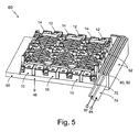
- Fig. 5 shows an embodiment of a device according to the invention in three-dimensional view.
- Fig. 1 shows the basic principle of the device as a circuit diagram. Shown here is a base element of a plurality of power electronic circuits a half-bridge circuit with two power semiconductor devices (20), here each formed as a transistor with an antiparallel connected diode. Such half-bridge circuits are the circuit-technical basis of a large number of different power semiconductor modules (10). Also shown are the first DC load connection elements (22, 24) of both polarities in the interior of the power semiconductor module (10), which are each connected to respectively assigned first connection elements (12, 14).
- an intermediate circuit capacitor (30) which serves in power electronic circuits of the intermediate storage of the energy before the supply to the power semiconductor components (20).
- This DC link capacitor (30) like a control unit (32) and at least one power semiconductor module (10), is often part of a more complex power electronic system (60).
- the power semiconductor module (10) has second connection elements (62, 64) for external connection as well as second direct current load connection elements (72, 74) of both polarities.
- a Y-capacitor (40) consisting of two discrete single capacitors (42, 44) is connected to the second connection elements (72, 74) of the complex system (60). It is also known to connect this Y-capacitor (40) to the corresponding first connection elements (12, 14) of the power semiconductor module (10).
- the two individual capacitors (42, 44) on the one hand with an associated DC load connection element (12, 14 or 72, 74) and on the other hand connected to ground potential (76).
- Fig. 2 schematically shows the embodiments of a device with a power semiconductor module (10) according to the prior art in a sectional view.
- a first molded body (50) here a heat dissipation device by way of example in an embodiment of a copper or aluminum body with a arranged thereon and against the heat dissipation device electrically but not thermally isolated substrate (52).
- the heat removal device (50) facing away from the surface of the substrate (52) has on an insulating body (54) on a plurality of conductor track (56) with different electrical potentials.
- Power semiconductor components (20) are arranged on some of these printed conductors (56) and connected in a circuit-compatible manner, by way of example by means of wire-bonding connections.
- a housing (90) surrounds the substrate (52) and has further connecting elements, shown here are two first direct current load connection elements (22, 24) of different potential. These first DC load connection elements (22, 24) connect, as known in the art, the associated tracks (56) of the substrate (52) to connection elements (12, 14) for external connection of the device.
- the illustration of an AC load connection element is omitted here as well as in the two following figures for clarity.
- the Y capacitor (40) is arranged here on an additional board (48) above the power semiconductor module (10).
- FIG. 3 and 4 schematically show two embodiments of a device according to the invention, each with a power semiconductor module (10) in a sectional view, starting from a device according to Fig. 2 ,
- the first direct current load connection elements (22, 24) are parallel to one another in each case in a section (220, 240), wherein these sections (220, 240) are at least partially flat, with parallel surface normals parallel to one another ,
- a second shaped body (80) here designed as a Z-shaped punched and bent part, is arranged such that a first part form body (82) is arranged between the two both sections (220, 240) of the first DC load connection elements (22, 24) come to rest.
- the first DC load connection elements (22, 24) are electrically isolated from each other as well as from the second molded body (80).
- the Z-shaped second shaped body (80) acts like a Y-capacitor (40) with one capacitor each (42, 44) between a first DC load connection element (22, 24) and the lying at ground potential first molded body (50).
- the second molded body (80) further has a second molded part body (84) on the electrically conductive with the first molded body (50), the heat dissipation device is connected.
- This connection is designed such that the entire second molded body (80) is displaceable parallel to the substrate (52) and thus to the parallel planar sections (220, 240) of the first DC load connection elements (22, 24). This is achieved in the simplest case by a slot-shaped recess in the second part of the molding (84).
- the capacitance of the two capacitors (42, 44) that have developed in this case can be adjusted and adapted to the respective application.
- the embodiment according to Fig. 4 has at the same time the same features no variable in its position second molded body.
- the second shaped body (80) is cup-shaped and encloses the substrate (52) on all sides with the heat-dissipating device, the first shaped body (50).
- the cup-shaped second shaped body (80) has recesses at a suitable point.
- these connecting elements (22, 24) opposite the second molded body (80) are electrically insulated.
- the embodiment is suitable Fig. 4 especially for shielding the substrate from high-frequency fields.
- Fig. 5 shows an embodiment of a device according to the invention in three-dimensional view, this device consists of a first molded body (50) of a plurality of power semiconductor modules (10), a capacitor unit and a control unit in a common housing. Shown here are only the essential components such as the first molded body (50), power semiconductor modules (10) and second DC load connection elements (72, 74) with indicated second connection elements (62, 46).
- the power modules (10) are in thermal conductive and electrically insulating connection with the first molded body (50).
- these second DC load connection elements (72, 74) extend inside the housing to the second Connection elements (62, 64), which serve for external contacting. As far as possible, these second DC load connection elements (72, 74) are arranged closely adjacent in their entire course in order to keep parasitic inductances small.
- these second direct current load connection elements (72, 74) here in the area adjacent to the power semiconductor modules (10) have a section in which they are flat and the surface normals of these surfaces are parallel to one another.
- These surfaces plates which are each assigned to a plate capacitor in the following.
- the arrangement of a second shaped body (80) which also has a two-dimensional partial molded body (82) between the two flat sections of the second DC load connection elements (72, 74) forms the second plate of a plate capacitor. Due to the electrically conductive, here integrally formed, connection of this second molded body (80) with the first on basic potential (46) lying first molded body (50) of the Y-capacitor (40) according to the circuit Fig. 1 educated.
Landscapes
- Engineering & Computer Science (AREA)
- Power Engineering (AREA)
- Inverter Devices (AREA)
- Power Conversion In General (AREA)
- Structure Of Printed Boards (AREA)
- Dc-Dc Converters (AREA)
Applications Claiming Priority (1)
| Application Number | Priority Date | Filing Date | Title |
|---|---|---|---|
| DE102009017621A DE102009017621B3 (de) | 2009-04-16 | 2009-04-16 | Vorrichtung zur Verringerung der Störabstrahlung in einem leistungselektronischen System |
Publications (1)
| Publication Number | Publication Date |
|---|---|
| EP2242102A1 true EP2242102A1 (fr) | 2010-10-20 |
Family
ID=42316013
Family Applications (1)
| Application Number | Title | Priority Date | Filing Date |
|---|---|---|---|
| EP10001494A Withdrawn EP2242102A1 (fr) | 2009-04-16 | 2010-02-13 | Dispositif de diminution de l'émission be bruit dans un système électronique de puissance |
Country Status (5)
| Country | Link |
|---|---|
| EP (1) | EP2242102A1 (fr) |
| JP (1) | JP5779319B2 (fr) |
| KR (1) | KR101695492B1 (fr) |
| CN (1) | CN101866906B (fr) |
| DE (1) | DE102009017621B3 (fr) |
Cited By (1)
| Publication number | Priority date | Publication date | Assignee | Title |
|---|---|---|---|---|
| US9576913B2 (en) | 2011-12-08 | 2017-02-21 | Fuji Electric Co., Ltd. | Semiconductor device and manufacturing method of semiconductor device |
Families Citing this family (8)
| Publication number | Priority date | Publication date | Assignee | Title |
|---|---|---|---|---|
| JP5609562B2 (ja) | 2010-11-10 | 2014-10-22 | ソニー株式会社 | 立体画像撮像装置 |
| DE102011076324B4 (de) * | 2011-05-24 | 2014-04-10 | Semikron Elektronik Gmbh & Co. Kg | Leistungselektronisches System mit Verbindungseinrichtung erster und zweiter Subsysteme |
| DE102011076325B4 (de) * | 2011-05-24 | 2016-05-04 | Semikron Elektronik Gmbh & Co. Kg | Kühlanordnung für eine leistungselektronische Komponente mit Subsystemen und einer Kühleinrichtung |
| DE102013104522B3 (de) * | 2013-05-03 | 2014-06-26 | Semikron Elektronik Gmbh & Co. Kg | Leistungshalbleitermodul mit Subeinheiten und Anordnung hiermit |
| US9646927B2 (en) | 2014-03-06 | 2017-05-09 | Mitsubishi Electric Corporation | Power semiconductor device |
| DE102015105347B4 (de) * | 2015-04-09 | 2022-03-24 | Semikron Elektronik Gmbh & Co. Kg | Anordnung mit einem leitstungselektronischen Bauteil und mit einer Gleichspannungsverschienung |
| EP3104507A1 (fr) * | 2015-06-12 | 2016-12-14 | ABB Technology AG | Agencement de terminaux pour module semi-conducteur de puissance |
| DE102019202728A1 (de) * | 2019-02-28 | 2020-09-03 | Robert Bosch Gmbh | Schaltungsanordnung zur Ansteuerung einer elektrischen Maschine |
Citations (10)
| Publication number | Priority date | Publication date | Assignee | Title |
|---|---|---|---|---|
| US20010043126A1 (en) * | 1999-07-15 | 2001-11-22 | Andrew Michael Cherniski | Electromagnetic interference blocking power bus bar |
| US6339192B1 (en) | 1997-12-12 | 2002-01-15 | Nec Corporation | Three-phase bus-bar structure having noise-filtering function |
| EP1191635A2 (fr) * | 2000-09-19 | 2002-03-27 | Nissan Motor Co., Ltd. | Structure de connection |
| EP1265282A2 (fr) | 2001-06-08 | 2002-12-11 | SEMIKRON Elektronik GmbH | Assemblage de circuits |
| US20030133282A1 (en) * | 2002-01-16 | 2003-07-17 | Beihoff Bruce C. | Power converter having improved EMI shielding |
| US20040246653A1 (en) * | 2003-06-09 | 2004-12-09 | Williams Kirt R. | Tunable capacitor |
| US20040257841A1 (en) * | 2003-06-18 | 2004-12-23 | Aisin Aw Co., Ltd. | Device for removing inverter noise |
| EP1657806A2 (fr) | 2003-08-21 | 2006-05-17 | Denso Corporation | Convertisseur de puissance et structure de montage de dispositif a semi-conducteur |
| EP1662568A2 (fr) * | 2004-11-24 | 2006-05-31 | General Electric Company | Module de puissance, branche de phase et onduleur à trois phase |
| DE102006006425A1 (de) | 2006-02-13 | 2007-08-23 | Semikron Elektronik Gmbh & Co. Kg | Leistungshalbleitermodul in Druckkontaktausführung |
Family Cites Families (9)
| Publication number | Priority date | Publication date | Assignee | Title |
|---|---|---|---|---|
| US20030085055A1 (en) * | 2001-11-05 | 2003-05-08 | Skinner Harry G | Substrate design and process for reducing electromagnetic emission |
| KR100488518B1 (ko) * | 2002-11-14 | 2005-05-11 | 삼성전자주식회사 | 반도체 장치의 방열 시스템 |
| US6906404B2 (en) * | 2003-05-16 | 2005-06-14 | Ballard Power Systems Corporation | Power module with voltage overshoot limiting |
| JP4075734B2 (ja) * | 2003-08-21 | 2008-04-16 | 株式会社デンソー | 半導体装置の実装構造 |
| US7157331B2 (en) * | 2004-06-01 | 2007-01-02 | Macronix International Co., Ltd. | Ultraviolet blocking layer |
| CN100539121C (zh) * | 2006-03-01 | 2009-09-09 | 乾坤科技股份有限公司 | 降低电磁波干扰的封装元件 |
| CN100590864C (zh) * | 2007-07-19 | 2010-02-17 | 威盛电子股份有限公司 | 传输线结构与信号传输结构 |
| JP4538474B2 (ja) * | 2007-08-06 | 2010-09-08 | 日立オートモティブシステムズ株式会社 | インバータ装置 |
| JP2009071130A (ja) * | 2007-09-14 | 2009-04-02 | Ihi Corp | コンデンサ内蔵非絶縁型半導体パワーモジュール |
-
2009
- 2009-04-16 DE DE102009017621A patent/DE102009017621B3/de active Active
-
2010
- 2010-02-13 EP EP10001494A patent/EP2242102A1/fr not_active Withdrawn
- 2010-04-06 JP JP2010087725A patent/JP5779319B2/ja active Active
- 2010-04-14 CN CN201010163339.5A patent/CN101866906B/zh active Active
- 2010-04-14 KR KR1020100034316A patent/KR101695492B1/ko active Active
Patent Citations (10)
| Publication number | Priority date | Publication date | Assignee | Title |
|---|---|---|---|---|
| US6339192B1 (en) | 1997-12-12 | 2002-01-15 | Nec Corporation | Three-phase bus-bar structure having noise-filtering function |
| US20010043126A1 (en) * | 1999-07-15 | 2001-11-22 | Andrew Michael Cherniski | Electromagnetic interference blocking power bus bar |
| EP1191635A2 (fr) * | 2000-09-19 | 2002-03-27 | Nissan Motor Co., Ltd. | Structure de connection |
| EP1265282A2 (fr) | 2001-06-08 | 2002-12-11 | SEMIKRON Elektronik GmbH | Assemblage de circuits |
| US20030133282A1 (en) * | 2002-01-16 | 2003-07-17 | Beihoff Bruce C. | Power converter having improved EMI shielding |
| US20040246653A1 (en) * | 2003-06-09 | 2004-12-09 | Williams Kirt R. | Tunable capacitor |
| US20040257841A1 (en) * | 2003-06-18 | 2004-12-23 | Aisin Aw Co., Ltd. | Device for removing inverter noise |
| EP1657806A2 (fr) | 2003-08-21 | 2006-05-17 | Denso Corporation | Convertisseur de puissance et structure de montage de dispositif a semi-conducteur |
| EP1662568A2 (fr) * | 2004-11-24 | 2006-05-31 | General Electric Company | Module de puissance, branche de phase et onduleur à trois phase |
| DE102006006425A1 (de) | 2006-02-13 | 2007-08-23 | Semikron Elektronik Gmbh & Co. Kg | Leistungshalbleitermodul in Druckkontaktausführung |
Cited By (1)
| Publication number | Priority date | Publication date | Assignee | Title |
|---|---|---|---|---|
| US9576913B2 (en) | 2011-12-08 | 2017-02-21 | Fuji Electric Co., Ltd. | Semiconductor device and manufacturing method of semiconductor device |
Also Published As
| Publication number | Publication date |
|---|---|
| JP5779319B2 (ja) | 2015-09-16 |
| KR20100114837A (ko) | 2010-10-26 |
| JP2010251750A (ja) | 2010-11-04 |
| CN101866906A (zh) | 2010-10-20 |
| DE102009017621B3 (de) | 2010-08-19 |
| CN101866906B (zh) | 2014-12-17 |
| KR101695492B1 (ko) | 2017-01-11 |
Similar Documents
| Publication | Publication Date | Title |
|---|---|---|
| DE102009017621B3 (de) | Vorrichtung zur Verringerung der Störabstrahlung in einem leistungselektronischen System | |
| DE102019133377B4 (de) | Wechselrichter mit kompakter bauform | |
| DE3837206C2 (de) | Elektrisches Schaltgerät | |
| DE10035613A1 (de) | Leistungsumwandlungsvorrichtung | |
| EP2997801B1 (fr) | Dispositif et module électrique permettant de convertir une tension continue en tension alternative | |
| DE102009011234A1 (de) | Elektronische Baugruppe | |
| EP2302782A1 (fr) | Agencement de convertisseur de courant | |
| WO2017108341A1 (fr) | Dispositif d'antiparasitage, sous-ensemble électronique et utilisation d'un dispositif d'antiparasitage | |
| DE102020006207A1 (de) | Motorantriebsvorrichtung mit Glättungskondensatoreinheit und Beschaltungskondensator | |
| DE202015004662U1 (de) | Zwischenkreiskondensatormodul mit niederinduktiven Busbar-Verbindungen | |
| DE102013216941B4 (de) | Gekühlte Kondensatoranordnung und Verwendung einer solchen | |
| DE10064969A1 (de) | Filtervorrichtung für mindestens eine von außen an ein Gehäuse anzuschließende elektrische Leitung | |
| DE102013203614A1 (de) | Kondensatoreneinheit | |
| DE102012201766B4 (de) | Leistungselektronisches System mit einem mindestens einen Einzug aufweisenden Gehäuse | |
| EP2341535B1 (fr) | Module semi-conducteur de puissance à contact de pression doté d'un accumulateur de pression hybride | |
| DE4338277A1 (de) | Flüssigkeitsgekühltes Stromrichtermodul mit Beschaltungsbauelementen für abschaltbare Leistungshalbleiter | |
| EP1480500B1 (fr) | Circuit d'alimentation en puissance avec supports de circuits tridimensionnelles ainsi que methode de fabrication | |
| DE102011053680A1 (de) | Schaltungsanordnung zur Verminderung von Oszillationsneigung | |
| EP4268552B1 (fr) | Dispositif de refroidissement destiné au refroidissement d'un module semi-conducteur et onduleur pourvu de dispositif de refroidissement | |
| DE102016202716B4 (de) | Halbleitermodul | |
| EP3240380B1 (fr) | Système de convertisseur | |
| AT413171B (de) | Halbleiter-bauelement mit einer kühlplatte | |
| EP3834591B1 (fr) | Agencement de circuit intermédiaire et onduleur | |
| DE102018221246A1 (de) | Halbleiter-Leistungsmodul und Verfahren zum Verbinden desselben mit anderen elektrischen Komponenten | |
| DE102010023191A1 (de) | Leistungsmodul sowie Montage eines Leistungsmoduls |
Legal Events
| Date | Code | Title | Description |
|---|---|---|---|
| PUAI | Public reference made under article 153(3) epc to a published international application that has entered the european phase |
Free format text: ORIGINAL CODE: 0009012 |
|
| 17P | Request for examination filed |
Effective date: 20100809 |
|
| AK | Designated contracting states |
Kind code of ref document: A1 Designated state(s): AT BE BG CH CY CZ DE DK EE ES FI FR GB GR HR HU IE IS IT LI LT LU LV MC MK MT NL NO PL PT RO SE SI SK SM TR |
|
| AX | Request for extension of the european patent |
Extension state: AL BA RS |
|
| STAA | Information on the status of an ep patent application or granted ep patent |
Free format text: STATUS: THE APPLICATION HAS BEEN WITHDRAWN |
|
| 18W | Application withdrawn |
Effective date: 20161108 |