EP1664896B1 - Elektrisch drehbarer mikrospiegel oder mikrolinse - Google Patents
Elektrisch drehbarer mikrospiegel oder mikrolinse Download PDFInfo
- Publication number
- EP1664896B1 EP1664896B1 EP04787320A EP04787320A EP1664896B1 EP 1664896 B1 EP1664896 B1 EP 1664896B1 EP 04787320 A EP04787320 A EP 04787320A EP 04787320 A EP04787320 A EP 04787320A EP 1664896 B1 EP1664896 B1 EP 1664896B1
- Authority
- EP
- European Patent Office
- Prior art keywords
- micro
- moving
- electrodes
- fixed
- electrode
- Prior art date
- Legal status (The legal status is an assumption and is not a legal conclusion. Google has not performed a legal analysis and makes no representation as to the accuracy of the status listed.)
- Expired - Lifetime
Links
- 238000004519 manufacturing process Methods 0.000 claims abstract description 8
- 239000010410 layer Substances 0.000 claims description 72
- 239000000758 substrate Substances 0.000 claims description 36
- 238000000034 method Methods 0.000 claims description 23
- 239000002344 surface layer Substances 0.000 claims description 23
- 238000005530 etching Methods 0.000 claims description 17
- 239000011810 insulating material Substances 0.000 claims description 8
- 239000003989 dielectric material Substances 0.000 claims description 6
- 238000009413 insulation Methods 0.000 claims description 6
- 238000001465 metallisation Methods 0.000 claims description 5
- 238000004804 winding Methods 0.000 claims description 4
- 238000010292 electrical insulation Methods 0.000 claims 2
- 230000015572 biosynthetic process Effects 0.000 claims 1
- 239000004065 semiconductor Substances 0.000 description 16
- 239000000463 material Substances 0.000 description 14
- 238000007747 plating Methods 0.000 description 11
- 238000002955 isolation Methods 0.000 description 9
- XUIMIQQOPSSXEZ-UHFFFAOYSA-N Silicon Chemical compound [Si] XUIMIQQOPSSXEZ-UHFFFAOYSA-N 0.000 description 8
- 239000010703 silicon Substances 0.000 description 8
- 229910052710 silicon Inorganic materials 0.000 description 8
- 230000007423 decrease Effects 0.000 description 7
- 230000000694 effects Effects 0.000 description 6
- 238000006073 displacement reaction Methods 0.000 description 5
- 230000003068 static effect Effects 0.000 description 5
- 230000003287 optical effect Effects 0.000 description 4
- 238000001312 dry etching Methods 0.000 description 3
- 230000000670 limiting effect Effects 0.000 description 3
- 229910052751 metal Inorganic materials 0.000 description 3
- 239000002184 metal Substances 0.000 description 3
- 230000001133 acceleration Effects 0.000 description 2
- 238000004026 adhesive bonding Methods 0.000 description 2
- 229910052782 aluminium Inorganic materials 0.000 description 2
- XAGFODPZIPBFFR-UHFFFAOYSA-N aluminium Chemical compound [Al] XAGFODPZIPBFFR-UHFFFAOYSA-N 0.000 description 2
- 239000012212 insulator Substances 0.000 description 2
- 230000010070 molecular adhesion Effects 0.000 description 2
- 239000008188 pellet Substances 0.000 description 2
- 239000011241 protective layer Substances 0.000 description 2
- 230000002829 reductive effect Effects 0.000 description 2
- 238000000926 separation method Methods 0.000 description 2
- 238000001039 wet etching Methods 0.000 description 2
- 229910052581 Si3N4 Inorganic materials 0.000 description 1
- VYPSYNLAJGMNEJ-UHFFFAOYSA-N Silicium dioxide Chemical compound O=[Si]=O VYPSYNLAJGMNEJ-UHFFFAOYSA-N 0.000 description 1
- BQCADISMDOOEFD-UHFFFAOYSA-N Silver Chemical compound [Ag] BQCADISMDOOEFD-UHFFFAOYSA-N 0.000 description 1
- 230000003044 adaptive effect Effects 0.000 description 1
- 239000000956 alloy Substances 0.000 description 1
- 229910045601 alloy Inorganic materials 0.000 description 1
- 238000005452 bending Methods 0.000 description 1
- 230000005540 biological transmission Effects 0.000 description 1
- 230000015556 catabolic process Effects 0.000 description 1
- 210000001520 comb Anatomy 0.000 description 1
- 230000003247 decreasing effect Effects 0.000 description 1
- 238000000151 deposition Methods 0.000 description 1
- 230000005684 electric field Effects 0.000 description 1
- 238000005265 energy consumption Methods 0.000 description 1
- 210000000887 face Anatomy 0.000 description 1
- 230000002349 favourable effect Effects 0.000 description 1
- PCHJSUWPFVWCPO-UHFFFAOYSA-N gold Chemical compound [Au] PCHJSUWPFVWCPO-UHFFFAOYSA-N 0.000 description 1
- 229910052737 gold Inorganic materials 0.000 description 1
- 239000010931 gold Substances 0.000 description 1
- 210000003128 head Anatomy 0.000 description 1
- 238000009434 installation Methods 0.000 description 1
- 238000005468 ion implantation Methods 0.000 description 1
- 238000005304 joining Methods 0.000 description 1
- 238000005459 micromachining Methods 0.000 description 1
- 229910021421 monocrystalline silicon Inorganic materials 0.000 description 1
- 150000004767 nitrides Chemical class 0.000 description 1
- 230000036961 partial effect Effects 0.000 description 1
- 230000000737 periodic effect Effects 0.000 description 1
- 238000000206 photolithography Methods 0.000 description 1
- 230000000750 progressive effect Effects 0.000 description 1
- 238000002310 reflectometry Methods 0.000 description 1
- 210000001525 retina Anatomy 0.000 description 1
- 238000007789 sealing Methods 0.000 description 1
- HQVNEWCFYHHQES-UHFFFAOYSA-N silicon nitride Chemical compound N12[Si]34N5[Si]62N3[Si]51N64 HQVNEWCFYHHQES-UHFFFAOYSA-N 0.000 description 1
- 229910052814 silicon oxide Inorganic materials 0.000 description 1
- 229910052709 silver Inorganic materials 0.000 description 1
- 239000004332 silver Substances 0.000 description 1
- 239000007787 solid Substances 0.000 description 1
- 238000010408 sweeping Methods 0.000 description 1
- 230000007704 transition Effects 0.000 description 1
- WFKWXMTUELFFGS-UHFFFAOYSA-N tungsten Chemical compound [W] WFKWXMTUELFFGS-UHFFFAOYSA-N 0.000 description 1
- 229910052721 tungsten Inorganic materials 0.000 description 1
- 239000010937 tungsten Substances 0.000 description 1
Images


Classifications
-
- G—PHYSICS
- G02—OPTICS
- G02B—OPTICAL ELEMENTS, SYSTEMS OR APPARATUS
- G02B26/00—Optical devices or arrangements for the control of light using movable or deformable optical elements
- G02B26/08—Optical devices or arrangements for the control of light using movable or deformable optical elements for controlling the direction of light
- G02B26/0816—Optical devices or arrangements for the control of light using movable or deformable optical elements for controlling the direction of light by means of one or more reflecting elements
- G02B26/0833—Optical devices or arrangements for the control of light using movable or deformable optical elements for controlling the direction of light by means of one or more reflecting elements the reflecting element being a micromechanical device, e.g. a MEMS mirror, DMD
- G02B26/0841—Optical devices or arrangements for the control of light using movable or deformable optical elements for controlling the direction of light by means of one or more reflecting elements the reflecting element being a micromechanical device, e.g. a MEMS mirror, DMD the reflecting element being moved or deformed by electrostatic means
Definitions
- the present invention relates to a micro-mirror or a micro-lens operable electrically in rotation.
- Micro-mirrors and micro-lenses resulting from micromachining techniques of semiconductor material are of great interest for the reflection or the transmission of a light beam thanks to the combination of their speed, their precision, their low energy consumption and their relatively low cost.
- micro-mirrors or microlenses can operate in two different modes which are the static or quasi-static mode and the oscillating mode.
- the micro-mirrors comprise a movable part, generally in the form of a plateau, provided with a reflecting zone.
- the microlenses comprise a perforated mobile part (that is to say in the form of a frame) on which is fixed a refracting lenticular piece forming a refractive zone.
- the moving part can take positions in which it is inclined at a fixed angle with respect to a rest position or it can move in rotation, its movement having a very small frequency in front of its resonant frequency.
- the reflected or transmitted light beam according to whether it is a micro-mirror or a micro-lens is pointed towards a user device and the field of application is, for example, optical routing systems or image projection systems.
- the mobile part oscillates at its resonance frequency, the reflected or transmitted light beam performs a periodic scan with an amplitude increased by the mechanical resonance phenomenon.
- the field of application is, for example, scanners in printers or barcode readers.
- the micro-mirrors can also be used in new applications such as the light beam scanning displays on the retina or the endoscopic confocal microscopes.
- Such micro-mirrors or microlenses conventionally comprise a mobile part, generally in the form of a plateau, provided with a main plane and having at least one reflecting zone for the micro-mirror and a refractive zone for the micro-lens, a fixed part, connecting means of the movable part to the fixed part embodying an axis substantially parallel to the main plane, electrical control means of the rotation of the movable portion about the axis.
- the optical quality of the micro-mirrors depends essentially on the flatness of their reflecting zone. That of microlenses depends on the precision of the shape of the lens, shape close to a sphere for example.
- the mobile part of the micro-mirrors generally comprises a micro-machined plate of semiconductor material forming the reflective zone or covered with at least one reflective layer and optionally a protective layer.
- the mobile part comprises a perforated plate supporting a lenticular refracting piece.
- the surface deformations may be induced by elements lying under the reflective zone or under the perforated plate supporting the lenticular piece. These elements, like electrodes, are very often used to generate the displacement of the mobile part, the stresses in the surface layer or layers of the mobile part (for example the reflective metal layer or the protective layer) and the dynamic deformations which occur during moving of the moving part.
- the size of the reflective zone must be sufficient to limit the diffraction effect of the light beam on its opening.
- Micro-mirrors typically larger than 500 micrometers are typically used. Of course such dimensions are not limiting, they actually depend on the application. These dimensional constraints are applicable to micro-lenses.
- micromirrors or microlenses are therefore intended to move in rotation about an axis substantially parallel to their main plane.
- Two or more micro-mirrors can be used in the same assembly to deflect the light beam several times. The same remarks apply to micro-lenses.
- Micro-mirrors actuated in rotation by electrostatic effect are known as that illustrated in FIGS. 1A, 1B.
- the moving part 1 is mounted on an axis of rotation 2 embodied by two aligned torsion arms 3 coming from the mobile part 1 and whose ends are secured to a fixed part 4.
- the movable part 1 faces the fixed part 4 while being at a distance in the rest position, it is represented by the dotted lines in FIG. 1A. It is suspended above the fixed part 4 by the torsion arms 3.
- Electric control means 5 for rotating the movable part 1 are provided. They comprise a mobile electrode 5.1 and two fixed counter-electrodes 5.2.
- the face of the moving part 1 which faces the fixed part 4 carries the moving electrode 5.1.
- the other face of the moving part 1 carries a reflecting zone 7.
- the fixed part 4 carries the two counter electrodes 5.2, 5.2 which face the moving electrode 5.1.
- the means 5 for controlling the rotational movement of the mobile part 1 also comprise means 5.4 of addressing (materialized by voltage sources) for applying an addressing signal in the form of an actuating voltage V1 or V2 between the moving electrode 5.1 and one or the other of the counter-electrodes 5.2 , 5.3.
- an electrostatic attraction force F (x) is generated and the moving part 1 moves in rotation about the axis 2, the moving electrode 5.1 being attracted by the counter electrode 5.2 or 5.3 which generated the potential difference V1 or V2.
- a problem posed by the electrostatic actuation is that the elastic restoring force (not shown), caused by the torsion arms 3, which opposes the displacement of the moving part is linear whereas the electrostatic attraction force is quadratic. .
- the attraction force takes over and a phenomenon of abrupt plating of the electrodes when the potential difference exceeds a certain threshold Vc or pull-in voltage (literally threshold voltage of attraction).
- Vc or pull-in voltage literally threshold voltage of attraction
- the controlled travel of the moving electrode corresponds to a distance that is largely restricted with respect to the initial distance separating the moving electrode 5.1 of the counter-electrodes 5.2, 5.3 in the rest position.
- This phenomenon limits the usable deflection of the moving part 1.
- a small space at rest between the moving electrode and the counter-electrodes will only allow a mobility with a very small angle, and the installation of a larger space at rest would involve the use of a very large actuating voltage, which is undesirable.
- the movement of the moving part is relatively limited.
- the document [1] shows another embodiment of a rotating micromirror capable of moving in a single direction during the attraction between two electrodes.
- This embodiment is illustrated in Figures 2A, 2B.
- the micro-mirror has substantially the same structure as before with a fixed part 4, a mobile part 1 located at rest at a distance from the fixed part 4, provided with a reflecting zone 7 and an axis of rotation 2 materialized by two torsion arm 3 whose ends are integral with the fixed part 4 and which come from the moving part 1.
- the difference with the previous example is at the level of the electrical control means 5 of the rotation of the movable part 1.
- the electrical control means 5 comprise a mobile electrode 50 issuing from the mobile part 1 and having a free end 50.1 and a fixed electrode 51 carried by the fixed part 4, opposite the mobile electrode 50 in the rest position.
- the movable electrode 50 is secured to an edge of the mobile part 1.
- the electrical control means 5 also include addressing means for applying an addressing signal in the form of an actuating voltage between the fixed electrode 51 and the moving electrode 50. These means are not shown so as not to overload the figures.
- the movable electrode 50 is relatively flexible, it is intended to be pressed gradually from its free end 50.1 on the fixed electrode 51.
- the movable electrode 50 is oriented substantially perpendicular to the axis of rotation 2.
- the Progressive plating phenomenon between the movable electrode 50 and the fixed electrode 51 is known by the name of "zipping effect".
- An electrically insulating layer (not visible in the figures) is generally interposed between the fixed electrode 51 and the moving electrode 50 to prevent the appearance of short circuits.
- the movable electrode 50 generally comprises a body 50.2 which ends with a primer 50.3 at its free end 50.1. The width of the primer 50.3 is greater than the width of the body 50.2 of the moving electrode 50.
- the addressing means apply an addressing signal, namely an actuating voltage between the moving electrode 50 and the fixed electrode 51, as long as this voltage is lower than the threshold voltage Vc, the electrode mobile 50 begins to approach the fixed electrode 51.
- the actuation voltage reaches the value Vc, a portion of the movable electrode 50 substantially corresponding to the primer 50.3 is reached. to stick on the fixed electrode 51.
- the movable portion 1 inclines at an angle ⁇ relative to the position it had at rest before the application of the actuating voltage. This angle is greater than a minimum angle ⁇ min whose meaning will be given later.
- the angle of inclination ⁇ of the movable part 1 and therefore of the reflecting zone 7 is substantially proportional to the actuation voltage applied between the fixed electrode 51 and the moving electrode 50.
- FIG. 2C represents the response curve (rotation angle ⁇ as a function of the operating voltage V applied between the fixed electrode 51 and the moving electrode 50) of such a micro-mirror.
- the actuating voltage can be reduced for the same angle of rotation.
- the force developed by the displacement of the moving part is inversely proportional to the square of the distance separating the moving electrode from the fixed electrode. But this distance is very small in the vicinity of the plated part of the moving electrode. This force is therefore very important in the range of use of the micro-mirror. This distance is at least equal to the thickness of the dielectric layer covering the fixed electrode. It is thus possible to rotate the moving part with angles of the order of 10 degrees with a moderate voltage typically less than about 100 V.
- the moving electrode In the rest position, the moving electrode must not be too far from the electrode fixed (a few micrometers to a few tens of micrometers) to limit the operating voltage, because the electrostatic force generated during the application of the operating voltage decreases rapidly when the distance between the two electrodes increases.
- a first disadvantage of such a device is that the moving part can not move in rotation on either side of the movable part.
- Another disadvantage of this type of actuation is that the moving part can not take certain orientations, these orientations correspond to angles ⁇ strictly included between 0 and ⁇ min.
- the axis of rotation 2 is offset with respect to the geometrical center of the mobile part 1.
- the offset is made so as to bring it closer to the moving electrode 50.
- This feature makes it possible to increase the travel of the movable part 1 while pushing the moment when it comes into abutment with the fixed part 4 which supports the fixed electrode 51. But, even with this feature, the movable part 1 always has a limited movement. There is a tendency to reduce the size of the moving part 1, but it is necessary to find a compromise between movement and size of the reflecting zone 7, the latter must have a size appropriate to the optical function that it must fulfill. It is often desirable for the reflecting zone 7 to have a span of between a few hundred micrometers and a few millimeters.
- control means are intended to deform the micromirror and not to move it in rotation.
- a micro-mirror whose electrical control means for the rotation comprise several pairs of interdigital electrodes 7.1, 7.2 in the form of combs.
- one of the comb electrodes 7.2 is secured to the fixed part 4.
- the other electrode 7.1 is secured via a hinge 8.1 of an arm 8 which is derived from the mobile part 1.
- This arm 8 is parallel to the torsion arm 3 secured to the fixed part 4 which contributes to materialize the axis of rotation.
- This type of actuation is very effective in the oscillating mode, thanks to the phenomenon of mechanical resonance, but is not well suited to operate in the static or quasi-static mode. In the static or quasi-static mode, this type of actuation is more efficient than the conventional electrostatic actuation but remains insufficient to obtain large angles of rotation.
- the movable interdigital electrode is integral with an arm 8 which is not the torsion arm has the disadvantage of moving the interdigitated electrode away from the axis of rotation and thus reducing the maximum deflection for an actuation voltage given.
- EP 1 193 528 and US 6,115,231 show a micro-mirror and a micro-relay, respectively, comprising a fixed electrode and a moving electrode.
- the object of the present invention is to propose a micro-mirror or a micro-lens capable of taking one or more static or quasi-static rotational positions that do not have the above limitations and difficulties. These limitations also applied to micro-lenses.
- an object of the invention is to provide a micro-mirror or a micro-lens capable of moving in rotation with a large amplitude and which can take a precise fixed position while maintaining a reduced actuation voltage.
- Another object of the invention is to provide a micro-mirror or a micro-lens which can take an angle of inclination in a wide range of angles, this range being continuous and extending on both sides its rest position corresponding to a zero inclination angle.
- Another object of the invention is to provide a micro-mirror or a micro-lens capable of taking a position which is not likely to introduce a vertical component to the movement of the central part of the reflecting zone of the micro-mirror or the refractive zone of the micro-lens, this central zone being generally that on which a light beam is reflected or transmitted.
- Another object of the invention is to provide a micro-mirror or a micro-lens whose movable portion is larger than in conventional micro-mirrors or microlenses.
- the present invention provides a micro-mirror or a micro-lens comprising a movable part with a reflective zone or a refractive zone respectively, a fixed part, means for connecting the moving part to the fixed part showing an axis of rotation contained in the movable portion, substantially parallel to a main plane of the movable portion, and electrical control means of the rotation of the movable portion about the axis.
- the electrical control means comprise two or more actuators, each formed of a fixed electrode integral with the fixed part and of a mobile electrode provided with a free end and an end connected to an arm.
- the mobile electrode being adapted to progressively tap on the fixed electrode from its free end when an actuating voltage is applied between the two electrodes of one of the actuators, the plating being done on a variable surface depending on the voltage applied between the electrodes of the actuator, the actuators being disposed on either side of the axis.
- the moving part can move in rotation with a maximum amplitude double that existing in the configuration described in document [1].
- An amplitude greater than about plus or minus 10 degrees can be obtained, more than 20 degrees total.
- the connecting means of the mobile part to the fixed part may be two torsion arms from of the movable part whose ends are connected to the fixed part.
- the axis can pass through the geometric center of the moving part, which avoids introducing a vertical component to the movement of the central zone of the movable part.
- a driving arm is offset relative to a torsion arm. But it is particularly advantageous to increase the travel that a torsion arm and a drive arm are in the extension of one another.
- At least one torsion arm has a cross section smaller than that of a drive arm.
- several mobile electrodes can be connected to the same drive arm.
- each drive arm may be integral with a single movable electrode.
- a moving electrode to be wound on itself, its free end being in a central zone of the winding.
- a rectilinear moving electrode configuration is also possible.
- a movable electrode configuration which makes it possible to reduce the voltage necessary to obtain the plating of the moving electrode on the fixed electrode of an actuator is that the moving electrode comprises a body of substantially constant width extending by a primer at level of its free end, the width of the primer being greater than that of the body.
- the fixed part may comprise a base and amounts on which support the connecting means of the movable part to the fixed part, the movable part being suspended above the base.
- the base may comprise a recess facing the movable portion which is then suspended above the recess.
- the fixed electrodes can be covered with a dielectric material.
- the control means may comprise addressing means capable of applying an actuating voltage to the moving electrodes and / or to the fixed electrodes of an actuator.
- the operating voltage may be a DC voltage superimposed on a variable control voltage.
- At least one fixed electrode of an actuator to be split up into two portions, one end portion of which, these two portions being isolated from one another, the means of addressing being able to apply a DC voltage to the end portion and a variable control voltage to the other portion.
- the DC voltage may be a minimum voltage to maintain a plating of the free end of the moving electrode of the actuator on the fixed electrode.
- control voltage applied to an actuator on one side of the axis When the control voltage applied to an actuator on one side of the axis is non-zero, the control voltage applied at the same time to an actuator located on the other side of the axis may be zero.
- isolation trenches can be made in step a) in the superficial layer and in the upper insulating layer at the first region of the fixed part and the first region of the moving part. and in the intermediate layer during step d) at the level of movable electrodes and the second region of the movable portion for electrically isolating the moving electrodes upon application of the actuating voltage to a moving electrode via the first region of the fixed portion and the first region of the movable portion .
- Step b) may include etching the recess in a central portion of the recessed portion.
- Step b) may be followed by a step of producing a layer of insulating material on the second etched substrate.
- the second region of the moving part can directly make the reflecting zone of the micro-mirror or a metallization step of the second region of the moving part can be provided to realize the reflecting zone of the micro-mirror.
- micro-lens it is possible to engrave the mobile part in the form of a frame during step b).
- the second insulating layer may be removed.
- the thickness of the superficial layer is chosen to be greater than the intermediate layer so as to obtain suitable torsion characteristics for the torsion arms.
- the first substrate may advantageously be a double SOI substrate and comprise next to the second insulating layer is a base semiconductor layer which is removed after the two substrates have been assembled.
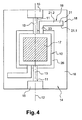
- the micro-mirror or the micro-lens comprises a movable portion 10 and a fixed portion 14.
- the movable portion 10 generally takes the form of a plate or a frame respectively. It is intended to be rotated about an axis 12.
- the axis passes through the movable portion 10 and is substantially parallel to a main plane of the movable portion 10. Connecting means 13 of the movable portion 10 to the fixed part 14 materialize this axis 12.
- These connecting means can take the form of two torsion arms 13 from the movable portion 10 and which have an end 11 secured (for example by embedding) of the fixed portion 14 at uprights 15
- the two torsion arms 13 are in the extension of one another.
- the uprights 15 of the fixed part 14 rest on a base 16 which extends under the moving part 10.
- the mobile part 10 is thus suspended above the fixed part 14 at its base 16.
- the movable part 10 comprises main faces, one of which is turned towards the fixed part 14 at its base 16 and the other end of which has a reflecting zone 17 (hatched in Figure 4) for reflecting light in the case of a micro-mirror.
- the reflective zone 17 is shown as occupying only partially the face of the moving part 10 but it could occupy it completely.
- the zone 17 represents a refractive zone, it may be a lenticular refracting piece fixed, for example by gluing, to the frame 10.
- the axis 12 may pass through the geometric center of the movable part 10.
- the micro-mirror or the micro-lens also comprises electric control means 18 for the rotational displacement of the mobile part 10.
- These means 18 comprise at least two actuators 19 with "zipping effect” and addressing means (not visible in Figure 4) of these actuators.
- actuator 19 zipping effect means an actuator formed of a pair of electrodes 20, 21 with a fixed electrode 20 and a movable electrode 21 having a free end 21.1, the movable electrode 21 being intended to come to press on the fixed electrode 20 from its free end 21.1, the plating being done on a variable surface according to a voltage applied between the two electrodes.
- the moving electrode 21 is therefore flexible.
- the fixed electrode 20 of the actuators 19 is secured to the fixed portion 14 at the base 16. It is not visible in Figure 4, it is hidden by the movable electrode 21. It is visible in Figure 5B .
- the movable electrode 21 of the actuators 19 is secured at its other end to an arm drive 23 which is derived from the movable portion 10 and which is directed substantially parallel to the axis of rotation 12. This drive arm 23 is sufficiently rigid. Thus the movable electrode 21 is no longer directly attached to the movable portion 10 as in the examples of Figures 2, it is shifted.
- the free ends 21.1 of the movable electrodes 21 of the two actuators 19 are located on either side of the axis of rotation 12.
- the actuators 19 are therefore arranged on either side of the axis 12
- each of the actuators 19 can drive the moving part 10 in one direction or the other, which makes it possible to increase its travel compared with the example of FIGS. else of the rest position (zero angle) can be obtained with an operating voltage typically less than 100V.
- the actuators 19 can be addressed or actuated either separately or simultaneously as will be seen later.
- the movable portion 10 may have a span between a few hundred micrometers and a few millimeters and a thickness of about a few tens of micrometers. It must have sufficient rigidity so that the reflecting or refracting zone 17 that it carries remains as stable as possible so as to maintain its optical quality whatever the conditions and especially during acceleration. These dimensions are not limiting of course.
- the movable electrode 21 may take the form from the drive arm 23, a substantially rectilinear body 21.2 of substantially constant width terminating at its free end 21.1 by an end portion 21.3 which may be of the same width that the body 21.2 or advantageously that can be wider. In the latter case the end portion 21.3 can be qualified as a primer. This primer 21.3 is visible in FIG. 5A.
- the fixed electrode 20 it can have any shape insofar as the mobile electrode 21 can be pressed on it.
- the primer 21.3 serves to reduce the threshold voltage of attraction Vc as well as the cutoff threshold voltage Vd.
- the actuator When the actuator is at rest, it is not subjected to any actuating voltage. Its mobile and fixed electrodes 20, 21 are separated by a space 25 which can be full of a gas (air or other) or which can be empty. This inter-electrode gap 25 is illustrated in FIG. 5B. This space 25 may be delimited by a cavity that contribute to form the amounts in the form of a frame as will be seen later.
- this space 25 It is preferable to place in this space 25 a layer of dielectric material 24 interposed between the fixed electrodes 20 and the moving electrodes 21 to avoid a short circuit when a movable electrode 21 comes into contact with a fixed electrode 20.
- This dielectric layer 24 is visible in FIG. 5B, it covers the fixed electrodes 20.
- the thickness of the dielectric layer 24 is between a minimum value and a maximum value. The minimum value is determined by the breakdown of the insulator subjected to an electric field generated by a given actuation voltage applied between the two electrodes of an actuator. The maximum value is determined by the maximum distance by which the two electrodes of an actuator can be located when the moving part 10 is in the rest position without the attraction force being too low for a given actuating voltage . For example, for an actuating voltage of 100 V, the minimum thickness of the dielectric layer 24 (made for example of oxide or nitride of a semiconductor material, silicon for example) will be about 0.2 micrometer .
- the movable electrode 21 may have a length of between a few tens of micrometers and a few millimeters, a thickness of between a few tenths of micrometers and a few micrometers, and a body width 21.2 much greater than its thickness.
- the thickness makes the movable electrode 21 sufficiently flexible in a direction substantially perpendicular to the surface of the base 16. If there is a primer 21.3, the latter is larger than the width of the body 21.2.
- the inter-electrode gap may be from a few micrometers to a few tens of micrometers.
- the base 16 comprises facing the mobile part 10 a recess 26.
- the movable portion 10 is able to enter the recess 26 when the movable portion 10 takes a sloped position with a large angle. The taking of an inclined position with such an angle of inclination would not be possible in the absence of the recess 26 because the movable portion 10 would hit the base 16.
- the fixed electrodes 20 are located on the base 16 to the outside of the recess 26 so as to maintain the relatively low inter-electrode space 25 in the rest position of the actuators.
- the depth of the recess is chosen to be sufficient for the mobile part to be inclined at an angle ⁇ max without striking the base 16.
- the angle ⁇ max corresponds to the maximum angle taken by the moving part when the addressing means (described later) deliver a maximum operating voltage.
- the recess 26 may be a hole through the base 16 or only a blind hole in the base 16. If it is a through hole, it may be made from the face of the base 16 intended to receive the fixed electrodes 20 (this face is said front face) or from the other face of the base 16 which is called back face. This recess 26 will rather be achieved by wet etching than dry etching in the material of the base 16 which is generally a semiconductor material.
- the distance d between the axis of rotation 12 and the fixed part 14 at the level of the plating surface must be relatively large (for example greater than about 50 micrometers) if it is desired to large inclination angle (eg greater than 5 °).
- the uprights supporting the torsion arms 13 take the form of a frame 15.1 which surrounds the mobile part 10 and the actuators 19 and which is integral with the base 16.
- This variant is shown in Figures 5A and 5B.
- This frame 15.1 can contribute to delimiting a cavity. It is preferred to limit the area occupied by this cavity so as to facilitate a step of sealing two substrates, which will be described later in the description of an exemplary method for producing a micro-mirror or a micro-lens. according to the invention.
- the driving arms 23 may be distinct from the torsion arms 13 as in FIG. 4. In this configuration, a torsion arm and a driving arm situated on one and the same side of the movable part are offset relative to one another. to the other. This is not of course an obligation as illustrated in Figure 5A. In this figure, the drive arm 23 is closer to the movable portion 10 than is the torsion arm 13 which extends it. Subsequently, unless otherwise indicated, it is considered that a drive arm 23 and a torsion arm 13 are in the extension of one another.
- connection of the movable electrodes 21 to the drive arms 23 is as close as possible to the axis of rotation 12 so as to allow a large clearance of the movable portion 10 while maintaining the inter-electrode space Actuators 19 relatively low.
- the actuators 19 can be located on either side of the movable part 10, but this is not an obligation, one could consider having only one pair of actuators 19 with the actuators 19 located on the same side of the movable part 10. Referring to FIG. 5A, only two of the four actuators shown could be represented, for example those corresponding to the section of FIG. 5B.
- the torsion arms 13 are in the extension of the driving arms 23.
- a torsion arm 13 has a cross section smaller than that of a driving arm 23; cross section gives it some flexibility in torsion.
- the drive arm 23 has a larger cross section to remain rigid during training.
- the dimensioning of the torsion arms 13 can be optimized so that they are sufficiently flexible in torsion and sufficiently stiff in vertical flexion. They are advantageously relatively thick and their width will be less than their thickness. If the torsion arm 13 is not rigid enough in vertical bending, the actuator 19 will tend to pull the movable portion 10 down rather than rotate it. The movement of the mobile part 10 may then not be a pure rotation, which can give a lateral translational movement to a reflected or transmitted light beam resulting from an incident light beam on the reflective or refractive zone 17.
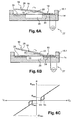
- Figs. 6A, 6B and the graph of Fig. 6C It is assumed that in this first mode of operation, the actuators 19 located on either side of the axis 12 are actuated separately.
- Addressing means 27 actuate either one or more actuators located on one side of the axis 12, or one or more actuators located on the other side of the axis 19.
- a first addressing signal namely an actuating voltage V1 between the two fixed and movable electrodes 20 of one of the actuators 19 (or several actuators located in the same position).
- V1 an actuating voltage between the two fixed and movable electrodes 20 of one of the actuators 19 (or several actuators located in the same position).
- the mobile part 10 and therefore the reflective or refractive zone 17 has turned abruptly by an angle ⁇ greater than + ⁇ min (+ ⁇ min represents the minimum angle of inclination taken by the mobile part 10 with respect to its position of rest).
- the edge of the movable portion 10 being on the same side of the axis (that is to say the torsion arm 13) that the movable electrode 21 which is pressed against the fixed electrode 20, is lowered and the opposite edge rises.
- the movable electrode 21 is more and more plate on the fixed electrode 20. There is propagation of the plating towards the drive arm 23. The plating surface is close to the arm 23.
- the movable part 10 inclines more and more until reaching an angle + ⁇ max which corresponds, in a favorable case, to a position in which the entire movable electrode 21 is pressed onto the fixed electrode. 20 if the movable portion 10 does not strike before the bottom of the recess 26.
- the angle ⁇ max corresponds in the best case to the angle taken by the moving part when the addressing means apply the maximum addressing voltage.
- the moving part 10 adopts the same behavior as before but in opposite direction, the movable electrode 21 gradually separates from the fixed electrode 20.
- the operating voltage V1 reaches the threshold voltage Vd detachment, only the end 21.1 of the movable electrode 21 remains plated on the fixed electrode 20.
- the angle ⁇ decreases. It is when this voltage Vd is applied that the mobile part 10 takes the position + ⁇ min. This voltage Vd is lower than the voltage Vc.
- the movable electrode 21 is detached from the fixed electrode 20 and the movable portion 10 resumes its substantially horizontal rest position. The actuating voltage V1 is then canceled.
- the addressing means 27 apply a second addressing signal to actuate the and / or other actuators 19 located on the other side of the axis 12 (left in the figures) namely a V2 actuating voltage (not shown) the movable portion 10 tilts in the opposite direction.
- the inclination is made from an angle ⁇ greater than - ⁇ min to an angle - ⁇ max plus the actuating voltage V2 is increased.
- the actuation voltage V2 is decreased, the inclination angle ⁇ decreases until it reaches - ⁇ min.
- the mobile part 10 can then move in rotation in two ranges of angles [- ⁇ max, - ⁇ min] and [+ ⁇ min, + ⁇ max] disjoint and / or take a fixed position in these beaches.
- the range of angles [- ⁇ min, + ⁇ min] can not be explored. It is not possible to obtain a continuous scan of the mobile part 10 in the range of angles [- ⁇ min, + ⁇ min]. This last beach is not exploitable for the mobile part 10.
- V1 and V2 are never different from zero together.
- the electrodes of an actuator begin to approach each other, the inclination of the mobile part is small but not zero. It would of course be possible for the addressing means 27 to simultaneously actuate actuators 19 located on either side of the axis 12.
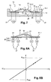
- FIG. 7 shows a second mode of operation of the micro-mirror or the micro-lens according to the invention.
- the addressing means 27 now apply a first actuating voltage V1 to the electrodes 20, 21 of one or more actuators 19 located on one side of the axis 12 (in the example on the right) and simultaneously a second voltage V2 actuating the electrodes 20, 21 of one or more actuators 19 located on the other side of the axis 12 (eg left).
- V1 actuating voltage
- V2 actuating voltage
- the moving part 10 take all the possible inclinations lying in the angle range [- ⁇ max, + ⁇ max].
- the mobile part 10 can be animated with a sweeping movement in rotation between - ⁇ max, + ⁇ max.
- the control voltages V1 'and V2' are never zero at the same time. Suppose we want to rotate the moving part to the right. If V1 'is non-zero, the bonding of the moving electrode propagates to the right and the moving part turns to the right. But if at the same time, V2 'is also non-zero, the collage will also propagate on the left which opposes the rotation of the moving part to the right.
- the control voltages V1 'and V2' may be indifferently positive or negative.
- the addressing means 27 of the actuators 19 may act either at the fixed electrodes 20 or at the mobile electrodes 21 or at the two fixed electrodes 20 and mobile 21 but it is more complicated. Unaddressed electrodes are at ground potential. Since the actuation of the actuators on one side of the axis is independent of that on the other side of the axis, this implies that the fixed or moving electrodes 20 located on one side of the axis 12 electrically isolated from those located on the other side of the axis 12.
- This insulation can be done conventionally by depositing separate conductive tracks without connection, by isolation trenches, for example air trenches or trenches filled with a dielectric material in conductive zones, by ion implantation of doping zones opposite to that of the substrate in which these zones are implanted.
- conductive tracks joining them can be made on the base (not shown), under the dielectric layer 24, the mobile electrodes 21 being kept at the same potential (generally the ground potential) .
- the fixed electrodes 20 can be maintained at the same potential. In this case, the fixed electrodes 20 may be merged and form a single fixed electrode as will be seen later.
- FIG. 8B represents the response curve (rotation angle ⁇ as a function of the actuating voltages V1 'and V2' applied to the actuators right and left respectively of the micro-mirror or the micro-lens shown in Figure 8.
- the variation of the inclination angle is linear and continuous between - ⁇ max, + ⁇ max.
- Such a micro-mirror or such a micro-lens is particularly well adapted to a use in static or quasi-static mode with a frequency much lower than the mechanical resonance frequency with a large amplitude.
- use in resonant mode is possible if the operating voltages of the actuators are alternating (for example sinusoidal) substantially at the resonance frequency.
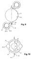
- Figure 9 shows a configuration variant for the fixed and movable electrodes 21 of an actuator 19 of a micro-mirror. It could of course be a micro-lens.
- the movable electrode 21 having a rectilinear body 21.2 with, if appropriate, a primer 21.3, it is possible for the electrode to be wound on itself substantially in a spiral, the free end 21.1 or the primer 21.3, if it exists, lying substantially in the center of the winding.
- This variant is illustrated in FIG. 9.
- the micro-mirror is thus more compact than with rectilinear moving electrodes 21. It would be the same for the micro-lens.
- the addressing means apply appropriate voltages on the moving electrodes of the actuators to move the moving part in rotation while the fixed electrodes are brought to a constant voltage. (usually the mass).
- a constant voltage usually the mass.
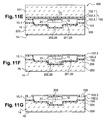
- the semiconductor substrates are conductive.
- a first substrate 100 is used formed of a base layer 101 of semiconductor material, for example silicon, covered with a sandwich 102 formed by two insulating layers 102.1, 102.2 (for example made of silicon oxide) located on either side of an intermediate layer 102.3 of semiconductor material (for example silicon), the sandwich 102 itself being covered by a surface layer 103 of semiconductor material (for example silicon).
- This substrate is illustrated in FIG. 11A.
- the insulating layer referenced 102.1 is the lower layer of the sandwich and the layer 102.2 is the upper layer of the sandwich.
- Such a substrate 100 may be a double SOI substrate (for Silicon on Insulator).
- the surface layer 103 is thicker than the intermediate layer 102.3.
- the layers of semiconductor material 101, 102.3, 103 are conductive.
- micro-mirror or micro-lens is similar to that of Figures 5A, 5B, the drive and torsion arms are end to end.
- a photolithography step defines the pattern of a first region of the fixed part 14, namely the frame 15.1 or the uprights, of a first region of the mobile part 10, of a first region of the torsion arms. 13 and drive 23. These different elements are then etched in the superficial layer 103 and in the upper insulating layer 102.2 ( Figure 11B).
- This etching step may be a dry etching step.
- the first regions are thus formed of the semiconductor material of the upper surface layer and the material of the insulating layer. If a micro-mirror is made, the moving part 10 remains full, whereas if a micro-lens is made, the moving part 10 is engraved like a frame with a central recess. This frame engraving is outlined in dotted lines in FIG. 11B.
- the moving electrodes of the actuators will be made in the intermediate layer 102.3 later.
- the torsion arms, the frame and the moving part will be used to route the addressing signals to the moving electrodes of the actuators. These addressing signals propagate in the frame and the torsion arms from contact pads carried by the frame and made subsequently.
- One of the torsion arms will be used for the addressing of the actuators located side of the axis and the other torsion arm for addressing the actuators located on the other side of the axis.
- the addressing signals for the moving electrodes on one side of the axis not to propagate to the moving electrodes on the other side of the axis that they must receive other addressing signals, in the superficial layer 103 and also in the upper insulating layer 102.2 (FIG.
- insulating trenches 104 are produced at the frame 15.1 and an isolation trench 106 at the first region of the mobile part 10. These trenches may be air trenches or may be subsequently filled with dielectric material. If instead of having a frame, two amounts are provided as in Figure 4, the latter are electrically isolated by their configuration.
- the isolation trenches 104 cut the frame 15.1 in two parts 105.1, 105.2, one 105.1 having to bear one of the contact pads transmitting one of the addressing signals and the other part 105.2 to carry the other transmitting contact pad the other addressing signal. The pads are not visible at this stage (FIG. 11C).
- the surface layer 103 corresponding to the first region of the movable part 10 is separated into two parts 107.1, 107.2 by the isolation trench 106.
- One of the torsion arms originates from one of the parts 107.1 and the other of the other part 107.2.
- the isolation trench 106 is directed in its majority along the axis of rotation 12. The isolation trench 106 is visible in FIG. 11C.
- a first recessed portion 201 is etched, which will contribute to forming the space Between fixed and movable electrodes actuators and possibly a second recessed portion 202 which will form the recess 26 to be located under the movable portion 10.
- the first recessed portion 201 is shallower than the second recessed portion 202.
- the second recessed portion 202 is located in a central zone of the first recessed portion 201. This etching may be a dry etching.
- the second substrate 200 thus etched will materialize the fixed electrodes 20 which are then combined for all the actuators.
- the fixed electrodes are thus included in the base.
- the second substrate 200 thus etched is then covered with a layer of insulating material 203, for example silicon nitride or an oxide (FIG. 11D).
- the layer of insulating material 203 materializes the insulating layer 24 inserted between fixed and movable electrodes 20.
- the two substrates 100, 200 are then fixed together by placing the first recessed portion 201 opposite the etched surface layer 103 (FIG. 11E).
- This fixation can be done by a method of molecular adhesion after preparing the surfaces to be assembled in a suitable manner.
- a method of molecular adhesion is known by the acronym SDB abbreviation Anglo-Saxon Silicon Direct Bonding.
- the second recessed part 202 is opposite with the first region of the movable part 10.
- the base layer 101 and the lower insulation layer 102.1 of the sandwich 102 of the first substrate 100 are removed by, for example, rough mechanical rectification followed by wet etching of the silicon.
- the intermediate layer 102.3 and the upper insulating layer 102.2 will then be etched to access the surface layer 103 so as to delimit contact pads.
- the zones thus etched are referenced 108 in FIG. 11G.
- Ground holes 103 are also etched in the superficial layer 103, which will be used, once metallized, to make resumptions of contact between the moving electrodes and the parts 107.1 and w1.07.1 of the first region of the moving part. 10.
- These vias 109 are dug in the torsion arms 13 in an area where they project from the movable portion 10 but other locations would be possible.
- metal is deposited so as to make the contact pads 110 and the contact resets 111 in the etched areas 108 and the vias 109 ( Figure 111).
- the deposited material may be tungsten, aluminum or any other metal or alloy conventionally used.
- FIGS. 11J and 11K show, in section and in plan view respectively, the result of an etching step in the intermediate layer 102.3 which aims to delimit the contour of the moving electrodes 21 with their primers 21.3 and their bodies 21.2, a second region of the movable portion 10, a second region of the torsion arms and drive arms (which are merged).
- the second region of the moving part, the second region of the torsion arms, the second region of the driving arms are thus formed in the semiconductor material of the intermediate layer 102.3.
- the first and second regions of the movable portion, torsion arms and drive arms are superimposed and thus form a stack of the surface layer of the upper insulating layer and the intermediate layer.
- an isolation trench 112 is provided between two mobile electrodes located on either side of the axis 12 and which are integral with the same torsion arm 13 and an isolation trench 113 between the mobile part 10 and the moving electrodes 21.
- Figure 11L is a section of the micro-mirror or micro-lens in a plane AA of Figure 11J. With reference to FIG. 11C, there are the contact pads 110 and the contact pickups 111.
- the reflecting zone 17 of the micro-mirror may be made by the semiconductor material of the intermediate layer 102.3 located at the second region of the mobile part 10 if it has sufficient reflectivity.
- micro-lens it is possible to relate, for example by gluing, a lenticular refractive pellet 17 to the frame forming the mobile part 10. It is assumed that this pellet is sketched in FIG. 11K. Area 17 could also represent the reflecting zone of the micro-mirror.
- micro-mirrors are conceivable.
- the number of actuators is not limited to two or four as illustrated. This number can be arbitrary, there is at least one actuator on one side of the axis and at least one actuator on the other side.
Landscapes
- Physics & Mathematics (AREA)
- General Physics & Mathematics (AREA)
- Optics & Photonics (AREA)
- Mechanical Light Control Or Optical Switches (AREA)
- Micromachines (AREA)
- Mechanical Optical Scanning Systems (AREA)
- Investigating Or Analysing Biological Materials (AREA)
Claims (63)
- Mikrospiegel mit einem eine Reflexionszone (17) umfassenden beweglichen Teil (10), einem festen Teil (14) und Verbindungseinrichtungen (13) des beweglichen Teils (10) mit dem festen Teil (14), eine in dem beweglichen Teil (10) enthaltene Rotationsachse (12) materialisierend, im wesentlichen parallel zu einer Hauptebene des beweglichen Teils (10), und elektrischen Einrichtungen (18) zu Steuerung der Rotation des beweglichen Teils (10) um die Achse (12),
dadurch gekennzeichnet, dass die elektrischen Steuerungseinrichtungen (18) zwei oder mehr Aktoren (19) umfassen, jeder gebildet durch eine feste Elektrode (20), fest verbunden mit dem festen Teil (14), und einer beweglichen Elektrode (21) mit einem freien Ende (21.1) und einem Ende, das mit einem Antriebsarm (23) verbunden ist, der im wesentlichen parallel ist zu der Achse (12) und aus einem Stück ist mit dem beweglichen Teil (10), wobei die bewegliche Elektrode (21) fähig ist, sich von ihrem freien Ende (21.1) aus progressiv an die feste Elektrode (20) zu schmiegen, wenn zwischen den beiden Elektroden (20, 21) eines der Aktoren (19) eine Betätigungsspannung (V1, V2) angelegt wird, und das Anschmiegen über eine variable Fläche erfolgt, in Abhängigkeit von der zwischen den Elektroden des Aktors angelegten Spannung, wobei die Aktoren beiderseits der Achse (12) angeordnet sind. - Mikrospiegel nach Anspruch 1, bei dem die Verbindungseinrichtungen des beweglichen Teils (10) mit dem festen Teil (14) zwei Torsionsarme (13) sind, die aus einem Stück mit dem beweglichen Teil (10) sind und deren Enden (11) mit dem festen Teil (14) verbunden sind.
- Mikrospiegel nach einem der Ansprüche 1 oder 2, bei dem die Achse (12) durch den geometrischen Mittelpunkt des beweglichen Teils (10) verläuft.
- Mikrospiegel nach einem der Ansprüche 2 oder 3, bei dem auf einer selben Seite des beweglichen Teils (10) ein Antriebsarm (23) versetzt ist in Bezug auf einen Torsionsarm (13).
- Mikrospiegel nach einem der Ansprüche 2 oder 3, bei dem eine selbe Seite des beweglichen Teils (10) einen Antriebsarm (23) und einen Torsionsarm (13) aufweist, von denen sich der eine jeweils in der Verlängerung des anderen befindet.
- Mikrospiegel nach Anspruch 5, bei dem der Torsionsarm (13) einen kleineren Querschnitt hat als der Antriebsarm (23).
- Mikrospiegel nach Anspruch 5, bei dem der Torsionsarm (13) einen in etwa gleichen Querschnitt hat wie der Antriebsarm (23).
- Mikrospiegel nach einem der Ansprüche 1 bis 7, bei dem mehrere bewegliche Elektroden (21) mit einem selben Antriebsarm (23) verbunden sind.
- Mikrospiegel nach einem der Ansprüche 1 bis 7, bei dem jeder Antriebsarm (23) mit einer einzigen beweglichen Elektrode (21) verbunden ist.
- Mikrospiegel nach einem der Ansprüche 1 bis 9, bei dem mehrere auf einer selben Seite der Achse (12) befindliche bewegliche Elektroden (21) in Höhe ihres freien Endes (21.1) miteinander verbunden sind.
- Mikrospiegel nach einem der Ansprüche 1 bis 10, bei dem wenigstens eine bewegliche Elektrode (21) um sich selbst gewickelt ist, wobei ihr freies Ende (21.1) sich in einer zentralen Zone der Wicklung befindet.
- Mikrospiegel nach einem der Ansprüche 1 bis 10, bei dem wenigstens eine bewegliche Elektrode (21) im wesentlichen geradlinig ist.
- Mikrospiegel nach einem der Ansprüche 1 bis 12, bei dem wenigstens eine bewegliche Elektrode (21) einen Rumpfteil (21.2) von im wesentlichen konstanter Breite hat, der an seinem freien Ende (21.1) durch einen Einleitungsteil (21.3) verlängert wird, wobei die Breite des Einleitungsteils (21.3) größer ist als die des Rumpfteils (21.2).
- Mikrospiegel nach einem der Ansprüche 1 bis 13, bei dem die festen Elektroden (20) der Aktoren (19) zusammenfallen.
- Mikrospiegel nach einem der Ansprüche 1 bis 14, bei dem der feste Teil (14) eine Basis (16) und vertikale Stützen (15) umfasst, an denen sich die Verbindungseinrichtungen (13) abstützen, so dass der mobile Teil (10) über der Basis (16) aufgehängt ist.
- Mikrospiegel nach Anspruch 15, bei dem die Basis (16) eine Vertiefung (26) gegenüber dem über ihr aufgehängten beweglichen Teil (10) umfasst.
- Mikrospiegel nach einem der Ansprüche 1 bis 16, bei dem die festen Elektroden (20) mit einem dielektrischen Material (24) überzogen sind.
- Mikrospiegel nach einem der Ansprüche 1 bis 17, bei dem die elektrischen Steuerungseinrichtungen (18) Ansteuerungseinrichtungen (27) umfassen, fähig eine Betätigungsspannung (V1, V2) an die beweglichen und/oder festen Elektroden zu legen.
- Mikrospiegel nach Anspruch 18, bei dem die Betätigungsspannung eine einer variablen Steuerspannung (V1', V'2) überlagerte Gleichstromspannung (V0) ist.
- Mikrospiegel nach Anspruch 18, bei dem mindestens eine feste Elektrode (20) eines Aktors in zwei Teilstücke (20.1, 20.2) aufgeteilt ist, wovon eines (20.1) das Endteilstück ist und diese beiden Teilstücke (20.1, 20.2) voneinander isoliert sind, wobei die Ansteuerungseinrichtungen (27) fähig sind, an das Endteilstück (20.1) eine Gleichspannung (V0) anzulegen und an das andere Teilstück (20.2) eine variable Spannung (V1', V2').
- Mikroschalter nach einem der Ansprüche 19 oder 20, bei dem die Gleichspannung (V0) eine Minimalspannung ist, um eine Anschmiegung des freien Endes (21.1) der beweglichen Elektrode (21) des Aktors auf der festen Elektrode (20) aufrechtzuerhalten.
- Mikroschalter nach einem der Ansprüche 19 bis 21, bei dem - wenn die an einen auf einer Seite der Achse befindlichen Aktor angelegte Steuerspannung nicht null ist -, die gleichzeitig an einen auf der anderen Seite der Achse befindlichen Aktor angelegte Steuerspannung null ist.
- Verfahren zur Realisierung eines Mikroschalters nach einem der Ansprüche 1 bis 22, dadurch gekennzeichnet, dass es die folgenden Schritte umfasst:a) Ätzen der Kontur eines ersten Bereichs des beweglichen Teils (10), eines ersten Bereichs des festen Teils (14), eines ersten Bereichs des Antriebsarms (23) und eines ersten Bereichs der Verbindungseinrichtungen (13) in einer Oberflächenschicht (103) und einer ersten Isolierschicht (102.2) eines Mehrschichtsubstrats (100), das einen alternierenden Stapel aus einer ersten und einer zweiten Isolierschicht (102.1, 102.2) und zwei Halbleiterschichten (103, 102.3) umfasst, von denen die eine eine Zwischenschicht (102.3) und die andere die Oberflächenschicht (103) ist;b) Ätzen - in einem zweiten Halbleitersubstrat (200) - eines Rücksprungteils (201), wobei dieses zweite Substrat (200) beiträgt zur Realisierung eines zweiten Bereichs des festen Teils (14) und der festen Elektroden (20) der Aktoren (19);c) Zusammenbau der beiden Substrate (100, 200), wobei der Rücksprungteil (201) der geätzten Oberflächenschicht (103) gegenübersteht;d) Ätzen der Kontur der beweglichen Elektroden (21), eines zweiten Bereichs des beweglichen Teils (10), eines zweiten Bereichs der Verbindungseinrichtungen (13), eines zweiten Bereichs der Antriebsarme (23) in der Zwischenschicht (102.3) und Vorabrealisierung der elektrisch mit den beweglichen Elektroden (21) verbundenen Metallisierungen (110, 111) zum Anlegen der Betätigungsspannung (V1, V2) jedes Aktors (19) über den festen Teil (14) und den beweglichen Teil (10).
- Verfahren nach Anspruch 23, bei dem man Isolationsgräben (104, 105) realisiert, in Schritt a) in der Oberflächenschicht (103) und der oberen Isolierschicht (102.1) in Höhe des ersten Bereichs des festen Teils (10) und des ersten Bereichs des beweglichen Teils (14), und in Schritt b) in der Zwischenschicht (102.3) in Höhe der beweglichen Elektroden (21) und dem zweiten Bereich des beweglichen Teils (10), um beim Anlegen der Betätigungsspannung an eine bewegliche Elektrode (21) über den ersten Bereich des festen Teils (14) und den ersten Bereich des beweglichen Teils (10) eine elektrische Isolation der beweglichen Elektroden (21) zu gewährleisten.
- Verfahren nach einem der Ansprüche 23 oder 24, in dem der Schritt b) das Ätzen der Vertiefung (26) in einem zentralen Teil des Rücksprungteils (201) umfasst.
- Verfahren nach einem der Ansprüche 23 bis 25, in dem auf den Schritt b) ein Schritt zur Realisierung einer Schicht aus Isoliermaterial (203) auf dem zweiten geätzten Substrat (200) folgt.
- Verfahren nach einem der Ansprüche 23 bis 26, dadurch gekennzeichnet, dass der zweite Bereich des beweglichen Teils (10) die Reflexionszone (17) realisiert.
- Verfahren nach einem der Ansprüche 23 bis 26, dadurch gekennzeichnet, dass es einen Schritt zu Metallisierung des zweiten Bereichs des beweglichen Bereichs (10) umfasst, um die Reflexionszone (17) zu realisieren.
- Verfahren nach einem der Ansprüche 23 bis 28, bei dem man nach dem Zusammenbau die zweite Isolierschicht (102.2) entfernt.
- Verfahren nach einem der Ansprüche 23 bis 29, bei dem die Oberflächenschicht (103) dicker ist als die Zwischenschicht (102.3).
- Verfahren nach einem der Ansprüche 23 bis 30, bei dem das erste Substrat (100) ein SOI-Doppelsubstrat ist und auf der Seite der zweiten Isolierschicht (102.2) eine Basishalbleiterschicht (101) umfasst, die nach dem Zusammenbau der beiden Substrate (100, 200) eliminiert wird.
- Mikrolinse mit einem eine Reflexionszone (17) umfassenden beweglichen Teil (10), einem festen Teil (14) und Verbindungseinrichtungen (13) des beweglichen Teils (10) mit dem festen Teil (14), eine in dem beweglichen Teil (10) enthaltene Rotationsachse (12) materialisierend, im wesentlichen parallel zu einer Hauptebene des beweglichen Teils (10), und elektrischen Einrichtungen (18) zu Steuerung der Rotation des beweglichen Teils (10) um die Achse (12), dadurch gekennzeichnet, dass die elektrischen Steuerungseinrichtungen (18) zwei oder mehr Aktoren (19) umfassen, jeder gebildet durch eine feste Elektrode (20), fest verbunden mit dem festen Teil (14), und einer beweglichen Elektrode (21) mit einem freien Ende (21.1) und einem Ende, das mit einem Antriebsarm (23) verbunden ist, der im wesentlichen parallel ist zu der Achse (12) und aus einem Stück ist mit dem beweglichen Teil (10), wobei die bewegliche Elektrode (21) fähig ist, sich von ihrem freien Ende (21.1) aus progressiv an die feste Elektrode (20) zu schmiegen, wenn zwischen den beiden Elektroden (20, 21) eines der Aktoren (19) eine Betätigungsspannung (V1, V2) angelegt wird, und das Anschmiegen über eine variable Fläche erfolgt, in Abhängigkeit von der zwischen den Elektroden des Aktors angelegten Spannung, wobei die Aktoren beiderseits der Achse (12) angeordnet sind.
- Mikrospiegel nach Anspruch 32, bei dem die Verbindungseinrichtungen des beweglichen Teils (10) mit dem festen Teil (14) zwei Torsionsarme (13) sind, die aus einem Stück mit dem beweglichen Teil (10) sind und deren Enden (11) mit dem festen Teil (14) verbunden sind.
- Mikrospiegel nach einem der Ansprüche 32 oder 33, bei dem die Achse (12) durch den geometrischen Mittelpunkt des beweglichen Teils (10) verläuft.
- Mikrospiegel nach einem der Ansprüche 33 oder 34, bei dem auf einer selben Seite des beweglichen Teils (10) ein Antriebsarm (23) versetzt ist in Bezug auf einen Torsionsarm (13).
- Mikrospiegel nach einem der Ansprüche 33 oder 34, bei dem eine selbe Seite des beweglichen Teils (10) einen Antriebsarm (23) und einen Torsionsarm (13) aufweist, von denen sich der eine jeweils in der Verlängerung des anderen befindet.
- Mikrospiegel nach Anspruch 36, bei dem der Torsionsarm (13) einen kleineren Querschnitt hat als der Antriebsarm (23).
- Mikrospiegel nach Anspruch 36, bei dem der Torsionsarm (13) einen in etwa gleichen Querschnitt hat wie der Antriebsarm (23).
- Mikrospiegel nach einem der Ansprüche 32 bis 38, bei dem mehrere bewegliche Elektroden (21) mit einem selben Antriebsarm (23) verbunden sind.
- Mikrospiegel nach einem der Ansprüche 32 bis 38, bei dem jeder Antriebsarm (23) mit einer einzigen beweglichen Elektrode (21) verbunden ist.
- Mikrospiegel nach einem der Ansprüche 32 bis 40, bei dem mehrere auf einer selben Seite der Achse (12) befindliche bewegliche Elektroden (21) in Höhe ihres freien Endes (21.1) miteinander verbunden sind.
- Mikrospiegel nach einem der Ansprüche 32 bis 41, bei dem wenigstens eine bewegliche Elektrode (21) um sich selbst gewickelt ist, wobei ihr freies Ende (21.1) sich in einer zentralen Zone der Wicklung befindet.
- Mikrospiegel nach einem der Ansprüche 32 bis 41, bei dem wenigstens eine bewegliche Elektrode (21) im wesentlichen geradlinig ist.
- Mikrospiegel nach einem der Ansprüche 32 bis 43, bei dem wenigstens eine bewegliche Elektrode (21) einen Rumpfteil (21.2) von im wesentlichen konstanter Breite hat, der an seinem freien Ende (21.1) durch einen Einleitungsteil (21.3) verlängert wird, wobei die Breite des Einleitungsteils (21.3) größer ist als die des Rumpfteils (21.2).
- Mikrospiegel nach einem der Ansprüche 32 bis 44, bei dem die festen Elektroden (20) der Aktoren (19) zusammenfallen.
- Mikrospiegel nach einem der Ansprüche 32 bis 45, bei dem der feste Teil (14) eine Basis (16) und vertikale Stützen (15) umfasst, an denen sich die Verbindungseinrichtungen (13) abstützen, so dass der mobile Teil (10) über der Basis (16) aufgehängt ist.
- Mikrospiegel nach Anspruch 46, bei dem die Basis (16) eine Vertiefung (26) gegenüber dem über ihr aufgehängten beweglichen Teil (10) umfasst.
- Mikrospiegel nach einem der Ansprüche 32 bis 47, bei dem die festen Elektroden (20) mit einem dielektrischen Material (24) überzogen sind.
- Mikrospiegel nach einem der Ansprüche 32 bis 48, bei dem die elektrischen Steuerungseinrichtungen (18) Ansteuerungseinrichtungen (27) umfassen, fähig eine Betätigungsspannung (V1, V2) an die beweglichen und/oder festen Elektroden zu legen.
- Mikrospiegel nach Anspruch 49, bei dem die Betätigungsspannung eine einer variablen Steuerspannung (V1', V'2) überlagerte Gleichstromspannung (V0) ist.
- Mikrospiegel nach Anspruch 49, bei dem mindestens eine feste Elektrode (20) eines Aktors in zwei Teilstücke (20.1, 20.2) aufgeteilt ist, wovon eines (20.1) das Endteilstück ist und diese beiden Teilstücke (20.1, 20.2) voneinander isoliert sind, wobei die Ansteuerungseinrichtungen (27) fähig sind, an das Endteilstück (20.1) eine Gleichspannung (V0) anzulegen und an das andere Teilstück (20.2) eine variable Spannung (V1', V2').
- Mikroschalter nach einem der Ansprüche 50 oder 51, bei dem die Gleichspannung (V0) eine Minimalspannung ist, um eine Anschmiegung des freien Endes (21.1) der beweglichen Elektrode (21) des Aktors auf der festen Elektrode (20) aufrechtzuerhalten.
- Mikroschalter nach einem der Ansprüche 50 bis 52, bei dem - wenn die an einen auf einer Seite der Achse befindlichen Aktor angelegte Steuerspannung nicht null ist -, die gleichzeitig an einen auf der anderen Seite der Achse befindlichen Aktor angelegte Steuerspannung null ist.
- Verfahren zur Realisierung eines Mikroschalters nach einem der Ansprüche 32 bis 53, dadurch gekennzeichnet, dass es die folgenden Schritte umfasst:a) Ätzen der Kontur eines ersten Bereichs des beweglichen Teils (10), eines ersten Bereichs des festen Teils (14), eines ersten Bereichs des Antriebsarms (23) und eines ersten Bereichs der Verbindungseinrichtungen (13) in einer Oberflächenschicht (103) und einer ersten Isolierschicht (102.2) eines Mehrschichtsubstrats (100), das einen alternierenden Stapel aus einer ersten und einer zweiten Isolierschicht (102.1, 102.2) und zwei Halbleiterschichten (103, 102.3) umfasst, von denen die eine eine Zwischenschicht (102.3) und die andere die Oberflächenschicht (103) ist;b) Ätzen - in einem zweiten Halbleitersubstrat (200) - eines Rücksprungteils (201), wobei dieses zweite Substrat (200) beiträgt zur Realisierung eines zweiten Bereichs des festen Teils (14) und der festen Elektroden (20) der Aktoren (19);c) Zusammenbau der beiden Substrate (100, 200), wobei der Rücksprungteil (201) der geätzten Oberflächenschicht (103) gegenübersteht;d) Ätzen der Kontur der beweglichen Elektroden (21), eines zweiten Bereichs des beweglichen Teils (10), eines zweiten Bereichs der Verbindungseinrichtungen (13), eines zweiten Bereichs der Antriebsarme (23) in der Zwischenschicht (102.3) und Vorabrealisierung der elektrisch mit den beweglichen Elektroden (21) verbundenen Metallisierungen (110, 111) zum Anlegen der Betätigungsspannung (V1, V2) jedes Aktors (19) über den festen Teil (14) und den beweglichen Teil (10).
- Verfahren nach Anspruch 54, bei dem man Isolationsgräben (104, 105) realisiert, in Schritt a) in der Oberflächenschicht (103) und der oberen Isolierschicht (102.1) in Höhe des ersten Bereichs des festen Teils (10) und des ersten Bereichs des beweglichen Teils (14), und in Schritt b) in der Zwischenschicht (102.3) in Höhe der beweglichen Elektroden (21) und dem zweiten Bereich des beweglichen Teils (10), um beim Anlegen der Betätigungsspannung an eine bewegliche Elektrode (21) über den ersten Bereich des festen Teils (14) und den ersten Bereich des beweglichen Teils (10) eine elektrische Isolation der beweglichen Elektroden (21) zu gewährleisten.
- Verfahren nach einem der Ansprüche 54 oder 55, dadurch gekennzeichnet, dass der Schritt b) das Ätzen von gelenkbildenden Einrichtungen (30.1) in Höhe des Rücksprungteils (201) umfasst.
- Verfahren nach einem der Ansprüche 54 bis 56, in dem der Schritt b) das Ätzen der Vertiefung (26) in einem zentralen Teil des Rücksprungteils (201) umfasst.
- Verfahren nach einem der Ansprüche 54 bis 57, in dem auf den Schritt b) ein Schritt zur Realisierung einer Schicht aus Isoliermaterial (203) auf dem zweiten geätzten Substrat (200) folgt.
- Verfahren nach einem der Ansprüche 54 bis 58, dadurch gekennzeichnet, dass der bewegliche Teil (10) während des Schritts b) in Form eines Rahmens geätzt wird.
- Verfahren nach Anspruch 59, dadurch gekennzeichnet, dass es einen Schritt des Zusammenbaus eines linsenförmigen lichtbrechenden Teils mit dem Rahmen des beweglichen Teils umfasst, um die lichtbrechende Zone (17) zu realisieren.
- Verfahren nach einem der Ansprüche 54 bis 60, bei dem man nach dem Zusammenbau die zweite Isolierschicht (102.2) entfernt.
- Verfahren nach einem der Ansprüche 54 bis 61, bei dem die Oberflächenschicht (103) dicker ist als die Zwischenschicht (102.3).
- Verfahren nach einem der Ansprüche 54 bis 62, bei dem das erste Substrat (100) ein SOI-Doppelsubstrat ist und auf der Seite der zweiten Isolierschicht (102.2) eine Basishalbleiterschicht (101) umfasst, die nach dem Zusammenbau der beiden Substrate (100, 200) eliminiert wird.
Applications Claiming Priority (2)
| Application Number | Priority Date | Filing Date | Title |
|---|---|---|---|
| FR0350508A FR2859541B1 (fr) | 2003-09-08 | 2003-09-08 | Micro-miroir actionnable electriquement en rotation |
| PCT/FR2004/002265 WO2005026814A1 (fr) | 2003-09-08 | 2004-09-07 | Micro-miroir ou micro-lentille actionnable electriquement en rotation |
Publications (2)
| Publication Number | Publication Date |
|---|---|
| EP1664896A1 EP1664896A1 (de) | 2006-06-07 |
| EP1664896B1 true EP1664896B1 (de) | 2007-11-14 |
Family
ID=34178989
Family Applications (1)
| Application Number | Title | Priority Date | Filing Date |
|---|---|---|---|
| EP04787320A Expired - Lifetime EP1664896B1 (de) | 2003-09-08 | 2004-09-07 | Elektrisch drehbarer mikrospiegel oder mikrolinse |
Country Status (7)
| Country | Link |
|---|---|
| US (1) | US7408695B2 (de) |
| EP (1) | EP1664896B1 (de) |
| JP (1) | JP4435164B2 (de) |
| AT (1) | ATE378617T1 (de) |
| DE (1) | DE602004010156T2 (de) |
| FR (1) | FR2859541B1 (de) |
| WO (1) | WO2005026814A1 (de) |
Families Citing this family (9)
| Publication number | Priority date | Publication date | Assignee | Title |
|---|---|---|---|---|
| JP4550653B2 (ja) * | 2005-04-15 | 2010-09-22 | 富士通株式会社 | マイクロ可動素子および光スイッチング装置 |
| FR2887537B1 (fr) * | 2005-06-23 | 2007-09-07 | Commissariat Energie Atomique | Actionneur electrostatique, dispositif comportant de tels actionneurs, microsysteme comportant un tel dispositif et procede de realisation d'un tel actionneur |
| JP4895196B2 (ja) * | 2007-01-10 | 2012-03-14 | セイコーエプソン株式会社 | アクチュエータ、光スキャナおよび画像形成装置 |
| JP2009063637A (ja) * | 2007-09-04 | 2009-03-26 | Fujifilm Corp | 光走査プローブおよび光走査プローブ装置並びに光走査プローブの制御方法 |
| EP2107038B1 (de) * | 2008-03-31 | 2012-05-16 | Imec | Elektrostatisch betätigbare MEMS-Vorrichtung mit verringerter Substrataufladung |
| US9025234B2 (en) * | 2009-01-22 | 2015-05-05 | E Ink California, Llc | Luminance enhancement structure with varying pitches |
| US9269536B2 (en) * | 2012-04-17 | 2016-02-23 | Varian Semiconductor Equipment Associates, Inc. | Double ended electrode manipulator |
| JP2020003629A (ja) * | 2018-06-28 | 2020-01-09 | パイオニア株式会社 | 光走査装置 |
| JP2023182992A (ja) * | 2022-06-15 | 2023-12-27 | セイコーエプソン株式会社 | デバイス構造、デバイス構造の製造方法 |
Family Cites Families (4)
| Publication number | Priority date | Publication date | Assignee | Title |
|---|---|---|---|---|
| US6115231A (en) * | 1997-11-25 | 2000-09-05 | Tdk Corporation | Electrostatic relay |
| US6496612B1 (en) * | 1999-09-23 | 2002-12-17 | Arizona State University | Electronically latching micro-magnetic switches and method of operating same |
| US6632374B1 (en) * | 2000-09-28 | 2003-10-14 | Xerox Corporation | Method for an optical switch on a silicon on insulator substrate |
| US6735004B1 (en) * | 2001-03-15 | 2004-05-11 | Nanogear, Inc. | Rotatable counterbalanced actuator |
-
2003
- 2003-09-08 FR FR0350508A patent/FR2859541B1/fr not_active Expired - Fee Related
-
2004
- 2004-09-07 EP EP04787320A patent/EP1664896B1/de not_active Expired - Lifetime
- 2004-09-07 WO PCT/FR2004/002265 patent/WO2005026814A1/fr not_active Ceased
- 2004-09-07 JP JP2006525170A patent/JP4435164B2/ja not_active Expired - Fee Related
- 2004-09-07 AT AT04787320T patent/ATE378617T1/de not_active IP Right Cessation
- 2004-09-07 US US10/570,586 patent/US7408695B2/en not_active Expired - Fee Related
- 2004-09-07 DE DE602004010156T patent/DE602004010156T2/de not_active Expired - Lifetime
Also Published As
| Publication number | Publication date |
|---|---|
| FR2859541B1 (fr) | 2005-10-14 |
| DE602004010156T2 (de) | 2008-09-04 |
| WO2005026814A1 (fr) | 2005-03-24 |
| US7408695B2 (en) | 2008-08-05 |
| US20070091406A1 (en) | 2007-04-26 |
| JP4435164B2 (ja) | 2010-03-17 |
| DE602004010156D1 (de) | 2007-12-27 |
| EP1664896A1 (de) | 2006-06-07 |
| FR2859541A1 (fr) | 2005-03-11 |
| ATE378617T1 (de) | 2007-11-15 |
| JP2007505335A (ja) | 2007-03-08 |
Similar Documents
| Publication | Publication Date | Title |
|---|---|---|
| EP1698041B1 (de) | Elektrostatische steuereinrichtung | |
| EP1519213B1 (de) | Bimorph angetriebener, schwingender Mikrospiegel | |
| US6201629B1 (en) | Torsional micro-mechanical mirror system | |
| EP1515119B1 (de) | Mikrohergestellte kreisel mit doppelter Stimmgabel | |
| US7329930B2 (en) | Micromechanical actuator with multiple-plane comb electrodes and methods of making | |
| US20030019832A1 (en) | Staggered torsional electrostatic combdrive and method of forming same | |
| EP3257808B1 (de) | Mikroelektromechanische und/oder nanoelektromechanische vorrichtung mit bewegung ausserhalb der ebene, die mit kapazitiven mitteln zur änderung der oberfläche ausgestattet ist | |
| WO2002065187A2 (fr) | Procede de fabrication d'un micro-miroir optique et micro-miroir ou matrice de micro-miroirs obtenus par ce procede | |
| FR2824643A1 (fr) | Dispositif de modulation de lumiere | |
| CN1296191A (zh) | 其中带有弹出反射镜的集成光电子装置及形成与操作方法 | |
| EP1664896B1 (de) | Elektrisch drehbarer mikrospiegel oder mikrolinse | |
| EP1562207B1 (de) | Mikroelektromechanisches System mit zwei stabilen Kipplagen | |
| Hah et al. | A self-aligned vertical comb-drive actuator on an SOI wafer for a 2D scanning micromirror | |
| EP1736435A1 (de) | Elektrostatischer Aktuator mit einem leitendem und hängendem Schwenkteil | |
| US20020008922A1 (en) | Actuator and micromirror for fast beam steering and method of fabricating the same | |
| Kim et al. | High fill-factor micromirror array using a self-aligned vertical comb drive actuator with two rotational axes | |
| EP1390793A2 (de) | Kippbarer optischer mikrospiegel, matrixanordnung für solche mikrospiegel und zugehöriges herstellungsverfahren | |
| EP3975588A1 (de) | Verfahren zur herstellung eines elektroakustischen transducers | |
| EP0754959B1 (de) | Mikroabtastelemente für optisches System | |
| TWI253436B (en) | Micromechanical actuator with multiple-plane comb electrodes and methods of making | |
| FR2865201A1 (fr) | Technique de realisation de structures a forte topologie auto-alignees | |
| WO2005069057A1 (fr) | Composants optiques et leur procede de realisation | |
| EP1381904A1 (de) | Optischer multipositionsschalter | |
| EP1746071A1 (de) | Mikroaktuator mit Balken mit gekrümmten Segmenten |
Legal Events
| Date | Code | Title | Description |
|---|---|---|---|
| PUAI | Public reference made under article 153(3) epc to a published international application that has entered the european phase |
Free format text: ORIGINAL CODE: 0009012 |
|
| 17P | Request for examination filed |
Effective date: 20060227 |
|
| AK | Designated contracting states |
Kind code of ref document: A1 Designated state(s): AT BE BG CH CY CZ DE DK EE ES FI FR GB GR HU IE IT LI LU MC NL PL PT RO SE SI SK TR |
|
| RIN1 | Information on inventor provided before grant (corrected) |
Inventor name: FILHOL, FABIEN Inventor name: DIVOUX, CLAIRE |
|
| RAP1 | Party data changed (applicant data changed or rights of an application transferred) |
Owner name: COMMISSARIAT A L'ENERGIE ATOMIQUE |
|
| DAX | Request for extension of the european patent (deleted) | ||
| GRAP | Despatch of communication of intention to grant a patent |
Free format text: ORIGINAL CODE: EPIDOSNIGR1 |
|
| RTI1 | Title (correction) |
Free format text: ELECTRICALLY ROTATABLE MICROMIRROR OR MICROLENS |
|
| RTI1 | Title (correction) |
Free format text: ELECTRICALLY ROTATABLE MICROMIRROR OR MICROLENS |
|
| GRAS | Grant fee paid |
Free format text: ORIGINAL CODE: EPIDOSNIGR3 |
|
| GRAA | (expected) grant |
Free format text: ORIGINAL CODE: 0009210 |
|
| AK | Designated contracting states |
Kind code of ref document: B1 Designated state(s): AT BE BG CH CY CZ DE DK EE ES FI FR GB GR HU IE IT LI LU MC NL PL PT RO SE SI SK TR |
|
| REG | Reference to a national code |
Ref country code: GB Ref legal event code: FG4D Free format text: NOT ENGLISH |
|
| REG | Reference to a national code |
Ref country code: CH Ref legal event code: EP |
|
| REG | Reference to a national code |
Ref country code: IE Ref legal event code: FG4D Free format text: LANGUAGE OF EP DOCUMENT: FRENCH |
|
| REF | Corresponds to: |
Ref document number: 602004010156 Country of ref document: DE Date of ref document: 20071227 Kind code of ref document: P |
|
| GBT | Gb: translation of ep patent filed (gb section 77(6)(a)/1977) |
Effective date: 20080130 |
|
| PG25 | Lapsed in a contracting state [announced via postgrant information from national office to epo] |
Ref country code: NL Free format text: LAPSE BECAUSE OF FAILURE TO SUBMIT A TRANSLATION OF THE DESCRIPTION OR TO PAY THE FEE WITHIN THE PRESCRIBED TIME-LIMIT Effective date: 20071114 Ref country code: ES Free format text: LAPSE BECAUSE OF FAILURE TO SUBMIT A TRANSLATION OF THE DESCRIPTION OR TO PAY THE FEE WITHIN THE PRESCRIBED TIME-LIMIT Effective date: 20080225 Ref country code: SE Free format text: LAPSE BECAUSE OF FAILURE TO SUBMIT A TRANSLATION OF THE DESCRIPTION OR TO PAY THE FEE WITHIN THE PRESCRIBED TIME-LIMIT Effective date: 20080214 |
|
| NLV1 | Nl: lapsed or annulled due to failure to fulfill the requirements of art. 29p and 29m of the patents act | ||
| PG25 | Lapsed in a contracting state [announced via postgrant information from national office to epo] |
Ref country code: SI Free format text: LAPSE BECAUSE OF FAILURE TO SUBMIT A TRANSLATION OF THE DESCRIPTION OR TO PAY THE FEE WITHIN THE PRESCRIBED TIME-LIMIT Effective date: 20071114 Ref country code: PL Free format text: LAPSE BECAUSE OF FAILURE TO SUBMIT A TRANSLATION OF THE DESCRIPTION OR TO PAY THE FEE WITHIN THE PRESCRIBED TIME-LIMIT Effective date: 20071114 Ref country code: FI Free format text: LAPSE BECAUSE OF FAILURE TO SUBMIT A TRANSLATION OF THE DESCRIPTION OR TO PAY THE FEE WITHIN THE PRESCRIBED TIME-LIMIT Effective date: 20071114 Ref country code: BG Free format text: LAPSE BECAUSE OF FAILURE TO SUBMIT A TRANSLATION OF THE DESCRIPTION OR TO PAY THE FEE WITHIN THE PRESCRIBED TIME-LIMIT Effective date: 20080214 |
|
| PG25 | Lapsed in a contracting state [announced via postgrant information from national office to epo] |
Ref country code: AT Free format text: LAPSE BECAUSE OF FAILURE TO SUBMIT A TRANSLATION OF THE DESCRIPTION OR TO PAY THE FEE WITHIN THE PRESCRIBED TIME-LIMIT Effective date: 20071114 |
|
| PG25 | Lapsed in a contracting state [announced via postgrant information from national office to epo] |
Ref country code: CZ Free format text: LAPSE BECAUSE OF FAILURE TO SUBMIT A TRANSLATION OF THE DESCRIPTION OR TO PAY THE FEE WITHIN THE PRESCRIBED TIME-LIMIT Effective date: 20071114 Ref country code: DK Free format text: LAPSE BECAUSE OF FAILURE TO SUBMIT A TRANSLATION OF THE DESCRIPTION OR TO PAY THE FEE WITHIN THE PRESCRIBED TIME-LIMIT Effective date: 20071114 |
|
| PG25 | Lapsed in a contracting state [announced via postgrant information from national office to epo] |
Ref country code: RO Free format text: LAPSE BECAUSE OF FAILURE TO SUBMIT A TRANSLATION OF THE DESCRIPTION OR TO PAY THE FEE WITHIN THE PRESCRIBED TIME-LIMIT Effective date: 20071114 Ref country code: SK Free format text: LAPSE BECAUSE OF FAILURE TO SUBMIT A TRANSLATION OF THE DESCRIPTION OR TO PAY THE FEE WITHIN THE PRESCRIBED TIME-LIMIT Effective date: 20071114 |
|
| PLBE | No opposition filed within time limit |
Free format text: ORIGINAL CODE: 0009261 |
|
| STAA | Information on the status of an ep patent application or granted ep patent |
Free format text: STATUS: NO OPPOSITION FILED WITHIN TIME LIMIT |
|
| PG25 | Lapsed in a contracting state [announced via postgrant information from national office to epo] |
Ref country code: PT Free format text: LAPSE BECAUSE OF FAILURE TO SUBMIT A TRANSLATION OF THE DESCRIPTION OR TO PAY THE FEE WITHIN THE PRESCRIBED TIME-LIMIT Effective date: 20080414 |
|
| REG | Reference to a national code |
Ref country code: IE Ref legal event code: FD4D |
|
| 26N | No opposition filed |
Effective date: 20080815 |
|
| PG25 | Lapsed in a contracting state [announced via postgrant information from national office to epo] |
Ref country code: IE Free format text: LAPSE BECAUSE OF FAILURE TO SUBMIT A TRANSLATION OF THE DESCRIPTION OR TO PAY THE FEE WITHIN THE PRESCRIBED TIME-LIMIT Effective date: 20071114 |
|
| PG25 | Lapsed in a contracting state [announced via postgrant information from national office to epo] |
Ref country code: GR Free format text: LAPSE BECAUSE OF FAILURE TO SUBMIT A TRANSLATION OF THE DESCRIPTION OR TO PAY THE FEE WITHIN THE PRESCRIBED TIME-LIMIT Effective date: 20080215 |
|
| BERE | Be: lapsed |
Owner name: COMMISSARIAT A L'ENERGIE ATOMIQUE Effective date: 20080930 |
|
| PG25 | Lapsed in a contracting state [announced via postgrant information from national office to epo] |
Ref country code: EE Free format text: LAPSE BECAUSE OF FAILURE TO SUBMIT A TRANSLATION OF THE DESCRIPTION OR TO PAY THE FEE WITHIN THE PRESCRIBED TIME-LIMIT Effective date: 20071114 Ref country code: MC Free format text: LAPSE BECAUSE OF NON-PAYMENT OF DUE FEES Effective date: 20080930 |
|
| REG | Reference to a national code |
Ref country code: CH Ref legal event code: PL |
|
| PG25 | Lapsed in a contracting state [announced via postgrant information from national office to epo] |
Ref country code: CY Free format text: LAPSE BECAUSE OF FAILURE TO SUBMIT A TRANSLATION OF THE DESCRIPTION OR TO PAY THE FEE WITHIN THE PRESCRIBED TIME-LIMIT Effective date: 20071114 Ref country code: BE Free format text: LAPSE BECAUSE OF NON-PAYMENT OF DUE FEES Effective date: 20080930 |
|
| PG25 | Lapsed in a contracting state [announced via postgrant information from national office to epo] |
Ref country code: CH Free format text: LAPSE BECAUSE OF NON-PAYMENT OF DUE FEES Effective date: 20080930 Ref country code: LI Free format text: LAPSE BECAUSE OF NON-PAYMENT OF DUE FEES Effective date: 20080930 |
|
| PG25 | Lapsed in a contracting state [announced via postgrant information from national office to epo] |
Ref country code: HU Free format text: LAPSE BECAUSE OF FAILURE TO SUBMIT A TRANSLATION OF THE DESCRIPTION OR TO PAY THE FEE WITHIN THE PRESCRIBED TIME-LIMIT Effective date: 20080515 Ref country code: LU Free format text: LAPSE BECAUSE OF NON-PAYMENT OF DUE FEES Effective date: 20080907 |
|
| PG25 | Lapsed in a contracting state [announced via postgrant information from national office to epo] |
Ref country code: TR Free format text: LAPSE BECAUSE OF FAILURE TO SUBMIT A TRANSLATION OF THE DESCRIPTION OR TO PAY THE FEE WITHIN THE PRESCRIBED TIME-LIMIT Effective date: 20071114 |
|
| PGFP | Annual fee paid to national office [announced via postgrant information from national office to epo] |
Ref country code: FR Payment date: 20101005 Year of fee payment: 7 Ref country code: IT Payment date: 20100922 Year of fee payment: 7 |
|
| PGFP | Annual fee paid to national office [announced via postgrant information from national office to epo] |
Ref country code: GB Payment date: 20100921 Year of fee payment: 7 |
|
| PGFP | Annual fee paid to national office [announced via postgrant information from national office to epo] |
Ref country code: DE Payment date: 20100922 Year of fee payment: 7 |
|
| GBPC | Gb: european patent ceased through non-payment of renewal fee |
Effective date: 20110907 |
|
| PG25 | Lapsed in a contracting state [announced via postgrant information from national office to epo] |
Ref country code: IT Free format text: LAPSE BECAUSE OF NON-PAYMENT OF DUE FEES Effective date: 20110907 |
|
| REG | Reference to a national code |
Ref country code: FR Ref legal event code: ST Effective date: 20120531 |
|
| REG | Reference to a national code |
Ref country code: DE Ref legal event code: R119 Ref document number: 602004010156 Country of ref document: DE Effective date: 20120403 |
|
| PG25 | Lapsed in a contracting state [announced via postgrant information from national office to epo] |
Ref country code: DE Free format text: LAPSE BECAUSE OF NON-PAYMENT OF DUE FEES Effective date: 20120403 |
|
| PG25 | Lapsed in a contracting state [announced via postgrant information from national office to epo] |
Ref country code: GB Free format text: LAPSE BECAUSE OF NON-PAYMENT OF DUE FEES Effective date: 20110907 Ref country code: FR Free format text: LAPSE BECAUSE OF NON-PAYMENT OF DUE FEES Effective date: 20110930 |