EP1665321B1 - Verfahren zur messung der beugungsmuster mit hilfe eines transmissionselektronenmikrosops zur ermittlung der kristallstruktur und vorrichtung hierfür - Google Patents
Verfahren zur messung der beugungsmuster mit hilfe eines transmissionselektronenmikrosops zur ermittlung der kristallstruktur und vorrichtung hierfür Download PDFInfo
- Publication number
- EP1665321B1 EP1665321B1 EP03750478A EP03750478A EP1665321B1 EP 1665321 B1 EP1665321 B1 EP 1665321B1 EP 03750478 A EP03750478 A EP 03750478A EP 03750478 A EP03750478 A EP 03750478A EP 1665321 B1 EP1665321 B1 EP 1665321B1
- Authority
- EP
- European Patent Office
- Prior art keywords
- intensities
- sample
- tem
- pattern
- measurement
- Prior art date
- Legal status (The legal status is an assumption and is not a legal conclusion. Google has not performed a legal analysis and makes no representation as to the accuracy of the status listed.)
- Expired - Lifetime
Links
- 238000000034 method Methods 0.000 title claims abstract description 59
- 239000013078 crystal Substances 0.000 title description 28
- 238000004627 transmission electron microscopy Methods 0.000 title description 3
- 238000002524 electron diffraction data Methods 0.000 claims abstract description 83
- 238000010894 electron beam technology Methods 0.000 claims abstract description 25
- 230000005540 biological transmission Effects 0.000 claims abstract description 10
- 238000005259 measurement Methods 0.000 claims description 73
- 238000002003 electron diffraction Methods 0.000 claims description 38
- 238000004458 analytical method Methods 0.000 claims description 17
- 230000015556 catabolic process Effects 0.000 claims description 3
- 238000006731 degradation reaction Methods 0.000 claims description 3
- 238000012544 monitoring process Methods 0.000 claims description 3
- 239000010453 quartz Substances 0.000 claims description 3
- VYPSYNLAJGMNEJ-UHFFFAOYSA-N silicon dioxide Inorganic materials O=[Si]=O VYPSYNLAJGMNEJ-UHFFFAOYSA-N 0.000 claims description 3
- 238000007599 discharging Methods 0.000 claims description 2
- 230000005855 radiation Effects 0.000 description 8
- 125000004429 atom Chemical group 0.000 description 6
- 238000003384 imaging method Methods 0.000 description 6
- 238000002441 X-ray diffraction Methods 0.000 description 5
- 230000000694 effects Effects 0.000 description 5
- 238000006243 chemical reaction Methods 0.000 description 4
- 239000000463 material Substances 0.000 description 4
- 239000000126 substance Substances 0.000 description 4
- 230000008901 benefit Effects 0.000 description 3
- 238000004422 calculation algorithm Methods 0.000 description 3
- 238000004364 calculation method Methods 0.000 description 3
- 238000005421 electrostatic potential Methods 0.000 description 3
- 239000000843 powder Substances 0.000 description 3
- UFHFLCQGNIYNRP-UHFFFAOYSA-N Hydrogen Chemical compound [H][H] UFHFLCQGNIYNRP-UHFFFAOYSA-N 0.000 description 2
- XEEYBQQBJWHFJM-UHFFFAOYSA-N Iron Chemical compound [Fe] XEEYBQQBJWHFJM-UHFFFAOYSA-N 0.000 description 2
- 230000008859 change Effects 0.000 description 2
- 230000006866 deterioration Effects 0.000 description 2
- 239000001257 hydrogen Substances 0.000 description 2
- 229910052739 hydrogen Inorganic materials 0.000 description 2
- 238000001683 neutron diffraction Methods 0.000 description 2
- 238000007670 refining Methods 0.000 description 2
- 238000013169 thromboelastometry Methods 0.000 description 2
- 241000252073 Anguilliformes Species 0.000 description 1
- 238000009825 accumulation Methods 0.000 description 1
- 230000004913 activation Effects 0.000 description 1
- 239000004411 aluminium Substances 0.000 description 1
- XAGFODPZIPBFFR-UHFFFAOYSA-N aluminium Chemical compound [Al] XAGFODPZIPBFFR-UHFFFAOYSA-N 0.000 description 1
- 229910052782 aluminium Inorganic materials 0.000 description 1
- QVGXLLKOCUKJST-UHFFFAOYSA-N atomic oxygen Chemical compound [O] QVGXLLKOCUKJST-UHFFFAOYSA-N 0.000 description 1
- 238000004590 computer program Methods 0.000 description 1
- 238000005564 crystal structure determination Methods 0.000 description 1
- 238000012866 crystallographic experiment Methods 0.000 description 1
- 238000013461 design Methods 0.000 description 1
- 238000001514 detection method Methods 0.000 description 1
- 230000005292 diamagnetic effect Effects 0.000 description 1
- 238000002050 diffraction method Methods 0.000 description 1
- 238000009792 diffusion process Methods 0.000 description 1
- 238000005430 electron energy loss spectroscopy Methods 0.000 description 1
- 125000004435 hydrogen atom Chemical group [H]* 0.000 description 1
- 230000006872 improvement Effects 0.000 description 1
- 238000003780 insertion Methods 0.000 description 1
- 230000037431 insertion Effects 0.000 description 1
- 229910052742 iron Inorganic materials 0.000 description 1
- 230000002427 irreversible effect Effects 0.000 description 1
- 230000002045 lasting effect Effects 0.000 description 1
- 230000007246 mechanism Effects 0.000 description 1
- 239000002159 nanocrystal Substances 0.000 description 1
- 150000002894 organic compounds Chemical class 0.000 description 1
- 239000001301 oxygen Substances 0.000 description 1
- 229910052760 oxygen Inorganic materials 0.000 description 1
- 239000002245 particle Substances 0.000 description 1
- 238000004445 quantitative analysis Methods 0.000 description 1
- 230000035945 sensitivity Effects 0.000 description 1
- 239000007787 solid Substances 0.000 description 1
- 230000005469 synchrotron radiation Effects 0.000 description 1
- 238000012546 transfer Methods 0.000 description 1
Images



Classifications
-
- H—ELECTRICITY
- H01—ELECTRIC ELEMENTS
- H01J—ELECTRIC DISCHARGE TUBES OR DISCHARGE LAMPS
- H01J37/00—Discharge tubes with provision for introducing objects or material to be exposed to the discharge, e.g. for the purpose of examination or processing thereof
- H01J37/26—Electron or ion microscopes; Electron or ion diffraction tubes
- H01J37/295—Electron or ion diffraction tubes
-
- G—PHYSICS
- G01—MEASURING; TESTING
- G01N—INVESTIGATING OR ANALYSING MATERIALS BY DETERMINING THEIR CHEMICAL OR PHYSICAL PROPERTIES
- G01N23/00—Investigating or analysing materials by the use of wave or particle radiation, e.g. X-rays or neutrons, not covered by groups G01N3/00 – G01N17/00, G01N21/00 or G01N22/00
- G01N23/20—Investigating or analysing materials by the use of wave or particle radiation, e.g. X-rays or neutrons, not covered by groups G01N3/00 – G01N17/00, G01N21/00 or G01N22/00 by using diffraction of the radiation by the materials, e.g. for investigating crystal structure; by using scattering of the radiation by the materials, e.g. for investigating non-crystalline materials; by using reflection of the radiation by the materials
- G01N23/20058—Measuring diffraction of electrons, e.g. low energy electron diffraction [LEED] method or reflection high energy electron diffraction [RHEED] method
Definitions
- the macroscopic material world is formed by millions of crystals; every crystal at a microscopic level is formed by a cell having some symmetry for example hexagonal, trigonal, cubic etc, and having a specified quantity of atoms therein whose positions are defined.
- every crystal at a microscopic level is formed by a cell having some symmetry for example hexagonal, trigonal, cubic etc, and having a specified quantity of atoms therein whose positions are defined.
- atomic resolution structural studies by means of X-Rays, neutron or electron diffraction.
- X-Ray diffraction is a technique which provides an average structure, usually of tens of thousands of particles. Newly synthesised materials are often in powder form and often present poor crystallinity for precise X-Ray structure determination.
- Electron diffraction is much more sensitive than X-Ray diffraction, providing about a ten thousand fold enhancement in signal.
- TEM transmission electron microscope
- a means for precise atomic structure analysis is linked to the increasing of reliability and precision in measuring ED intensity data.
- One important feature for accurate measurement of intensities in an ED pattern is ability of capture the high dynamic range of spot intensities, which can range between 1 and 10 6 for the weakest and most intense spots respectively.
- the intensities of the spots in an ED pattern need to be determined accurately with minimum beam damage to the sample.
- the precise measurement of about 50-100 reflections is sufficient to have an accurate picture of the crystal structure. This contrasts with X-Ray diffraction where several hundreds of reflections need to be measured.
- the precision of measuring ED intensities should be high and preferably the same for all reflections. This is true also for the weakest intensities (i.e. those resulting from large diffraction angles), since they have a significant influence on the accurate determination of the light atoms in the structure.
- EDC electron diffraction cameras
- the electrostatic potential distribution and the electron density may be reconstructed in some cases.
- the scanning system has a lot of limitations. For example, it takes several hours to record with precision the reflections of an ED pattern. Therefore, only very few beam resistant samples can be precisely measured with this technique.
- this type of scanning system is interfaced with EDCs whose beam size is generally too wide (micrometer range) for obtaining atom resolution detail.
- ED patterns of crystals may also be measured using a transmission electron microscope (TEM).
- TEM transmission electron microscope
- Structure analysis of crystals by ED in a TEM presents a lot of advantages over conventional X-Ray or neutron diffraction: the size of studied crystallites in TEM can be very small (even tens of Angstroms), therefore individual phases in powders (nm size) can be examined.
- a TEM is interfaced to a slow scan charged-coupled device (CCD) camera or imaging plate for recording the ED patterns.
- CCD charged-coupled device
- problems with using a CCD camera or imaging plate for detection exist.
- the dynamic range of the CCD camera is limited which leads to errors in measuring very intense or very weak intensities.
- continuous exposure of a CCD camera to high diffracted ED beam intensities can damage the CCD detector.
- Even, if in the near future those problems could be partially resolved in some commercial CCD cameras, the main problem of precision measurement (up to 1 %) of all ED intensities - and specially the weakest ones - will remain. For instance, accuracy in intensity estimation for high angle (> 5 Angstroms -1 ) reflections is very poor (up to 25 % accuracy).
- Imaging plates for recording ED in a TEM can be constructed with the same area as the photographic films, and may be used together with photographic film in a TEM. Exposed plates may read with a laser beam; this system is claimed to have dynamic range over 100 times more than that of a commercial CCD camera. As with CCD cameras, the main problem of precision measurement (up to 1 %) of all ED intensities -and specially the weakest ones - cannot be resolved with this technique.
- Document US 3,849,647 discloses a method for measuring electron diffraction patterns of a sample by using a TEM wherein the beam is scanned after the sample.
- Double conical beam-rocking system for measurement of integrated electron diffraction intensities by Vincent R. et al., Ultramicroscopy, Mar. 1994, Vol. 53, No 3, pages 271-282 .
- the present invention relates to a method for obtaining an electron diffraction pattern from any conventional transmission electron microscope (TEM) which overcomes the problems of dynamic range, speed at which intensities are measured and sample deterioration in the beam, accounting for beam instability from which method and devices of the prior art all suffer.
- the invention is suitable for measuring with high precision electron diffraction intensities, correct them from dynamical contributions, and perform calculations to derive crystal structures at atomic resolution from nanometer size areas, or in the range afforded by the beam size the TEM.
- the present invention is a method for measuring electron diffraction, ED patterns of a sample, said patterns suitable for structure determination therefrom using a transmission electron microscope, TEM, wherein the ED pattern is scanned by means of deflector coils in the TEM situated after the sample, wherein the electron beam is precessed by means of deflector coils in the TEM situated before the sample, in combination with a similar precession of the ED pattern by means of deflector coils situated after the sample.
- TEM transmission electron microscope
- Another embodiment of the present invention is a method as described above wherein parameters of step d) are one or more of:
- Another embodiment of the present invention is a method as described above wherein one or more Faraday cages are used to measure the reflections of the ED pattern during the measurement of intensities.
- Another embodiment of the present invention is a method as described above wherein a combination of a scintillator and a photomultiplier is used to analyse the ED pattern during measurement of intensities.
- Another embodiment of the present invention is a method as described above wherein a continuous dynode electron multiplier, CDEM, is used to analyse the ED pattern during measurement of intensities.
- CDEM continuous dynode electron multiplier
- Another embodiment of the present invention is a TEM-adapting device, comprising a scan generator and a precession signal generator in which the scan generator is configured to scan the ED pattern by means of deflector coils in the TEM situated after the sample, and wherein the precession signal generator is configured to precess the electron beam by means of deflector coils in the TEM situated before the sample, in combination with a similar precession of the ED pattern by means of deflector coils situated after the sample.
- Another embodiment of the present invention is a device as described above further comprising an inverter and adapter connected to the output of the signal precession generator.
- Another embodiment of the present invention is a device as described above further comprising a CCD camera and/or a diffractometer.
- Another embodiment of the present invention is a device as described above further comprising an insulated condenser diaphragm located in the path of beam, before the beam contacts the sample..
- Another embodiment of the present invention is a device as described above further comprising one or more Faraday cages, a combination of a scintillator and a photomultiplier, and/or a CDEM, each having an analogue-to-digital converting means.
- Another embodiment of the present invention is a device as described above further comprising a computer having a computer readable storage means which interfaces to one or more of the above devices.
- Another embodiment of the present invention is a device as described above further comprising a mounting enabling one or more Faraday cages, a combination of a scintillator and a photomultiplier, and/or a CDEM to be fitted at the bottom of the TEM column, and/or in the 35mm camera port, and/or in any available port.
- Another embodiment of the present invention is a device as described above further comprising a Faraday cage preamplifier that has a current leakage of between 1 and 50 femptoamperes.
- Another embodiment of the present invention is a use of a device as described above for measuring ED patterns of a sample, said patterns suitable for structure determination therefrom using a transmission electron microscope.
- Another embodiment of the present invention is a TEM comprising a device as described above.
- the present invention is a method and device that can interface to any TEM of the art or future TEM that enables said TEM to rapidly and precisely measure all ED reflections in any diffraction pattern of any zone axis, while minimizing the damage to radiation sensitive and non-radiation sensitive samples.
- the method and interface implement a scanning protocol in the TEM whereby the electron beam is deflected by means of deflector coils in the TEM which are situated after the sample,
- the method and interface comprise use of any CCD camera (such as a domestic video camera, web camera, a security camera, specialist CCD camera) which records an ED pattern resulting from a brief exposure of the sample to the beam, after which the beam is blanked.
- the data captured in this low dose mode by the CCD camera is used to preset parameters such as area to be scanned, precession mode, step size of scanning.
- the method and interface may also use a diffractometer in place of a CCD camera.
- the device which is used to measure intensities is called diiffractometer.
- the method and interface comprise use of a Faraday cage, a combination of a scintillator and a photomultiplier, or continuous dynode electron multiplier (CDEM) to record the ED pattern in order to obtain a crystal structure.
- a Faraday cage a combination of a scintillator and a photomultiplier, or continuous dynode electron multiplier (CDEM) to record the ED pattern in order to obtain a crystal structure.
- CDEM continuous dynode electron multiplier
- One embodiment of the present invention is a method for measuring electron diffraction (ED) patterns of a sample from a transmission electron microscope (TEM) wherein the ED pattern is scanned by means of deflector coils situated after the sample and wherein the electron beam is precessed by means of beam tilt coils in the TEM which are situated before the sample in combination with a similar precession of the ED pattern via deflection coil below the sample (Vincent and Midgley 1998).
- the diffraction pattern is moved in a step-by-step scanning mode across a motionless (fixed) detector.
- the invention represents an improvement on the methods known in the art for scanning, such as, for example, that disclosed by Avilov et al, 1999 in relation to an EDC.
- a sample according to the invention is any substance susceptible to crystallographic study. Examples include nanocrystals, powders.
- the measurement of ED intensities in a precession mode allows all ED intensities to be recorded under reduced influence from dynamical diffraction and double scattering contributions, so permitting structure analysis of improved precision.
- Methods for implementing a precession mode in a TEM are known in the art. By precessing an incident beam at a constant angle around a zone axis in combination with a similar precession of the ED pattern below the specimen (Vincent and Midgley 1998), the equivalent mechanism of the precession of the specimen is obtained.
- the reflections are swept successively through the Ewald sphere and the resulting integrated intensities are recorded by the system together with the angle of precession and the defection/scanning of all the ED spots.
- An aspect of the invention calculates the crystal structure resulting from said integrated intensities.
- the combination of the precession and scanning methods reduces the sensitivity of ED intensities to crystal thickness, reduces the effect of Ewald sphere curvature and can also reduce a lot of multiple beam dynamical effects contribution to the reflections. This way all ED reflections are much more kinematical in character e.g . a quality of structure analysis can be greatly improved.
- Any CCD camera may be used to record an ED pattern resulting from a brief exposure of the sample to the beam, after which the beam is blanked.
- the ED pattern captured by the CCD camera is used to preset parameters such as the step size in pixels, area to be scanned, precession mode activation which are used during the measurement of intensities with the diffractometer. By exposing the sample to the beam for a short period and subsequently blanking-off (shutting off) the beam, the sample is exposed to the damage of the electron beam for a very short period.
- the ED pattern captured by the CCD camera is not used to calculate the crystal structure, but is used to preset parameters for use during the measurement of intensities.
- the exposure may last for no longer than 1 ms, 2ms, 10ms, 100ms, 200ms, 1 s, 2 s, 5 s, 10 s, 20 s, 25 s, 30 s, 40 s, 50 s, or 60 s.
- measurement of intensities means the acquisition of an ED pattern which is transformable into structural data. Such data is measured by, for example, one or more Faraday cages, a combination of a scintillator and a photomultiplier, or a CDEM.
- measurements made by the aforementioned CCD camera are not usually taken during the measurement of intensities; measurements made by the CCD camera are usually taken prior to the measurement of intensities and are usually used to set parameters used during the measurement of intensities.
- the electron beam is precessed and/or the ED pattern scanned according to a method of the invention as described herein.
- An example of a parameter that may be set using the ED pattern captured by the CCD camera is one or several predermined sections of reciprocal space of the ED pattern that is recorded during the measurement of intensities.
- To record a whole ED pattern would be very time consuming and would lead to deterioration of the crystal.
- the TEM can be set up to record the whole ED pattern , or a preselected number of spots or areas of the reciprocal space, while minimizing beam damage to the sample. This way a complete set of intensities may be obtained from the same crystal and a complete set of structure factors with statistical precision of 1-2 % for complete structure determination.
- parameters that can be set using the ED pattern captured by the CCD camera are the number of scanning steps and the step size (in pixels).
- the information gathered by the CCD camera allows the user to choose these prior to the measurement of intensities, which constitutes a clear advantage in comparison with systems where the number of pixels is predefined. That way, structural aspects like superstructure reflections, satellite commensurate- incommensurate reflections or diffusion backgrounds can be refined in very precise way and separately to main structure reflections.
- the ED pattern captured by a diffractometer may also be used to monitor the stability of the measurement during the measurement of intensities.
- the stability of the measurement can be confirmed by frequently comparing the intensity of a particular reflection with the reference reflection determined by the ED pattern captured by the diffractometer. Since radiation damage alters drastically all intensities of ED pattern, radiation damage that alters the sample can be immediately detected. Furthermore, the effects of beam instability also affects the intensities of an ED pattern, therefore beam instability may be detected also. Thus, any beam instability or radiation damage can be incorporated into the structure calculation, so leading to structures of better precision. Alternatively, any beam instability may be detected during measurement of intensities and used to change parameters during the measurement of intensities.
- An isolated condenser diaphragm C2 may be used to monitor the beam current during the measurement of intensities.
- the measurements obtained from the isolated condenser diaphragm is used to monitor intensity drift of the primary beam, and to make adjustments to the resulting ED pattern or interpretation thereof.
- any beam instability may be detected during measurement of intensities and used to change parameters during the measurement of intensities. Since drift of the primary beam leads to inaccuracies of the resulting ED pattern, a method which monitors the primary beams leads to a more accurate ED pattern and hence structure.
- the isolated condenser diaphragm may be C1 or C2 aperture (located before the sample).
- Another aspect of the invention is a special diaphram holder suitable for placing the isolated condenser diaphragm in the beam.
- the method of monitoring the primary beam current using an isolated condensor diaphragm may be used in combination with any of the methods disclosed erein.
- the ED pattern may be scanned in x and y direction or in spiral mode following the symmetry of the ED pattern.
- One or more Faraday cages may be used to detect ED during the measurement of intensities.
- a combination of a scintillator and a photomultiplier may be used to detect ED during the measurement of intensities.
- a continuous dynode electron multiplier (CDEM) may be used to detect ED during the measurement of intensities.
- a combination of one or more of the aforementioned detectors may be used to detect ED during the measurement of intensities.
- the dynamic range (10 8 ) of one or more of these devices is sufficient for obtaining the desired precision.
- the measurement of intensity using a Faraday cage where applicable comprises the following steps:
- the method of the invention may be used to make one dimensional scans to measure, for example, the intensity versus radius in ring patterns from polycrystalline samples or it may be used to make two-dimensional x-y scans with intensities of small single crystals (spot ED patterns).
- the time taken to record intensity for a linear or two-dimensional scan increases with the angular resolution and the accuracy of the measurement that is desired .
- the reflection intensities can be measured as the sums of the intensities recorded at each point of the scanned profile.
- the computer of the system can carry out the measurement both in accumulation mode( to achieve the required statistical accuracy) or the constant -time mode.
- Another embodiment of the present is one or more devices that can be interfaced to a TEM that enables said TEM to measure ED patterns from a sample.
- said device is capable of connecting to a TEM which is not normally equipped for measuring ED patterns.
- a TEM might possess a set of deflection coils located before and after the sample, but the TEM might not be equipped with a set of amplifiers to drive the coils or with a device to generate precession or scanning signals.
- One or more devices according to the invention provides functionality to the TEM, enabling said TEM to perform a method of the invention.
- said device is capable of connecting to a TEM which is partially equipped for measuring ED patterns.
- a TEM might possess a set of deflection coils located before and after the sample, and with a set of amplifiers to drive the coils, but have no means to generate precession or scanning signals according to the invention.
- One or more devices according to the invention provides functionality to TEM, enabling said TEM to perform a method of the invention.
- Such TEM adapting device(s) comprises components which enable the TEM to perform one or more of the aforementioned methods separately or in combination.
- said device(s) enables the TEM to perform the scanning protocol and precession protocol and optionally record an ED pattern resulting from a brief exposure of the sample to the beam and optionally perform the measurement of intensities of ED patterns using one or more Faraday cages, a combination of a scintillator and a photomultiplier, or a CDEM.
- the device(s) and method according to the present invention enables any TEM to be adapted to measure atomic structures of materials. Since the electron beam in a TEM is about 10 4 times more intense than X-ray radiation, results from ED according to the invention are comparable in intensity to those obtained using Synchrotron radiation, without the expenditure or inconvenience associate with obtaining or being allocated time on a Synchrotron. Examples of devices include, but are not limited to those listed below. One or more of said devices may be incorporated in a single device.
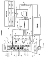
- FIG. 2 An example of a configuration of the components disclosed above is given in Figure 2 .
- all the devices mentioned above are shown, however, some may be absent, depending on which devices are already present in the TEM.
- the diffractometer, or the CCD camera may be present, both may be present or none may be present.
- isolated condenser diaphragm may be absent or present.
- the associated circuitry may be absent or present as determined by the skilled person and the circuitry available.
- Connections between the above mentioned devices may be direct or indirect; additional components may be inserted between device as known as understood by the skilled artisan.
- the diffractometer can be mounted in any available port of any TEM or inside the column of the TEM.
- ports include example on-axis, or on the 35 mm port.
- CCD camera may be positioned in a front of a window, on the 35 mm port or any port of the TEM suitable for capturing an image of an ED pattern.
- the CCD camera or diffractometer connects to the computer directly or via an analogue to digital converter.
- the invention may include a mounting for the detector for the measurement of intensities, the design of which enables the user to obtain high precision ED pattern intensities, even if the position below the projection chamber is unavailable because of possible existence of CCD cameras or energy filters.
- a mounting for the detector for the measurement of intensities the design of which enables the user to obtain high precision ED pattern intensities, even if the position below the projection chamber is unavailable because of possible existence of CCD cameras or energy filters.
- one or more Faraday cages, a combination of a scintillator and a photomultiplier, or a CDEM can be fitted at the bottom of the TEM column or in the 35mm camera port.
- the flexibility of the mounting even enables a detector to be directly fitted to an EELS spectrometer (e.g . of Wien type), allowing an energy filtered diffraction pattern to be obtained.
- the advantage of precise intensity measurement of such filtered ED pattern is that one can not only has access to the crystal structure and the chemical bonding , but also
- all types of diffraction patterns can be measured (e.g . ring type from polycrystalline samples, spot diffraction patterns from any single crystal zone axis orientation, texture patterns).
- the inventors have found that the precision in measurement of ED intensities is adjustable up to 1 % in intensity or better for both high intense and low intense reflections, so allowing a very precise structure determination that enables even hydrogen atoms to be revealed in the structure and/or the type of crystal bonding.
- the computer controls the scanning and/or precession protocols and records the ED patterns from both the CCD camera or diffractometer, and the Faraday cage(s), a combination of a scintillator and a photomultiplier, and/or CDEM.
- One aspect of the invention is an algorithm that allows data obtained from the CCD camera or diffractometer to be used to present parameters used in the measurement of intensities.
- All ED intensity data that are measured by the system can be automatically controlled via computer, which after performing various mathematical operations for crystal structure refinement will automatically propose to the user one ( or several ) crystallographic models for the studied sample.
- the invention may make use of an algorithm that transforms the raw data, enabling the calculation and refining of cell parameters by least squares, calculate Patterson and Fourier maps for structural model refinement.
- the algorithm also uses direct methods (including maximum entropy methodology) to find the atomic locations into the structure (including light atoms such as H) and reconstruct the electrostatic potential using both Fourier methods and atomic or ionic kappa models to reveal the nature of crystal bonding.
- the software of the system can also read ED patterns recorded with CCD cameras, diffractometers or imaging plates, therefore it can be easily interfaced with those systems to constitute a complete metrology system of measuring ED intensities and refining crystal structures.
- Figure 1 represents a possible arrangement of one or more devices of the invention and a TEM.
- a TEM 1 comprises a gun 2, which emits electrons which pass proximal to a series of coils or lenses (5 to 16) which focus and deflect the beam.
- Indicated in Figure 1 is a cross-section through the lens; since the lenses are circular coils, the view depicts two cross-sections for each coil and labeled are the right hand cross-sections for each coil.
- the coils are condenser stigmator coils (CSC) 5, deflection and beam tilt coils (DBTC) 6, objective stigmator and alignment coils 7, diffraction stigmator coils (DSC) 8, diffraction and intermediate alignment coils (DIAC) 9, a first condenser 10, a second condenser 11, the upper part of the objective lens 12, the lower part of the objective lens 13, the diffraction lens 14, the intermediate lens 15, the projective lens 16.
- the CSC 5 is situated in the second condenser coil 11.
- the DBTC 6 contains a rotation alignment coil, a deflection coil and a beam tilt coil; it is situated in the upper part of the objective lens 12.
- the DIAC 9 is the last coil used for scanning the diffraction image onto the diffractometer according to one aspect of the invention.
- the TEM may also comprise a 35mm port 17 through which a diffractometer or a CCD camera of the invention may be inserted as described above.
- a diffractometer with a retractable Faraday cage 18 is inserted in the 35 mm port 17.
- the TEM may also comprise a window in the projection chamber 20.
- a CCD camera of the invention 19 is positioned such that it takes a diffraction image through the window of the projection chamber 20.
- the TEM may also comprise a fluorescent screen 21.
- FIG. 1 Shown in Figure 1 is a mechanical interface, MID, 22 of the invention to which a Faraday cage, FC, 23 may be coupled.
- the FC 23 may be used to measure intensities.
- Another aspect of the invention is an isolated condenser diaphragm and holder 3 ; this special diaphragm holder with isolated condenser diaphragm is used to measure the primary beam stability of the microscope and may be inserted into the C2 beam aperture.
- Shown also in the figure is the specimen 4.
- Figure 2 represents a possible arrangement of a device of the invention, together with a TEM. Arrows 1 to 23 are the same as for Figure 1 .
- a TEM according to the invention may also comprise an electronic rack of amplifiers 26 which connects to one or more lenses, for example, the DBTC 24 (for controlling precession) and to the DIAC 25 (for controlling scanning and descanning of the diffraction image). Should the TEM not already comprise such a rack of amplifiers, said rack of amplifiers 26 may a device of the invention.
- An interface 29, is a device that adjusts the output of the precession signal generator and/or the scan generator circuits 30 such that they are suitable for input into the coils of the TEM.
- the TEM may be equipped with an electronic rack of amplifiers 26, in which case the interface 29 provides a signal suitable for input into said amplifiers.
- the electronic rack of amplifiers 26 may be absent from the TEM, in which case said electronic rack of amplifiers 26 may be a device of the invention or integrated into the interface.
- the electronic rack of amplifiers 26 may be connected to the interface 29 via one or more cables 28.
- the interface 29 may also be connected via one or more cables 27 to the optional isolated condenser diaphragm 3, to record primary beam current.
- the interface 29, may be connected via one or more cables 37, to a printed circuit board 30 that contains components connected and configured to generate scan and precession signals.
- the circuit board is connected to a computer 31.
- the circuit board 30 may be of a type that can slot directly into a computer as is shown in the figure e.g .
- the CCD camera 19 connects to the computer via one or more cables 34; the connection may be any such as, for example, serial, parallel, SCSI, USB, Firewire etc.
- the Faraday cage used to measure intensities 23, is connected to a high precision, high dynamic range, high speed pre-amplifier 35, said preamplifier amplifying the output of the Faraday cage 23 so enabling measurement of the intensity of the ED pattern.
- the Faraday cage 18 is optionally connected to the preamplifier 35 via one or more cables 36.
- the output of the preamplifier 35 is connected to the computer 31 via one or more cables 33.
- the preamplifier may also comprise an analogue to digital (A/D) converter.
- the output of the amplifier in the example shown is digital and may be configured to connect directly to a computer port, e.g . serial, parallel, SCSI, USB, Firewire.
- the personal computer 32 has a computer readable medium, that contains an image of software suitable for performing as necessary one or more of the following tasks: setting scan generator parameters 32A, setting precession signal parameters 32B, recording and analyzing a data obtained via CCD/diffractometer 32C, recording an ED pattern obtained via a Faraday cage 32D, analysing the diffraction image(s) 32E.
- Figure 3 represents a detail of the invention depicting a TEM 1, connected to an electronic rack of amplifiers 26, which in turn is connected to an interface 29, which in turn is connected to a printed circuit board 30.
- the TEM comprises at least DBTC 6, OSDAC 7, DSC 8 and DIAC 9.
- a device of the invention controls the DBTC 6 and the DIAC 9; furthermore, only illustrated are components for precessing the beam and scanning the diffraction image in the X-direction; those components for precession the beam and scanning the diffraction image in the Y-direction, connected to the TEM via 47 and 48, are not shown for clarity, but would be similar or identical.
- an electronic rack 26 Connected to the DBTC 6 and the DIAC 9 via one or more cables 46 and 49 respectively is an electronic rack 26 comprising amplifiers 39.
- the resistors 40 allow the signals from the precession signal generator 41 and the scan generator 43 to connect and be compatible with the amplifiers 39 of the electronic rack 26.
- a printed circuit board 30 Connected to the interface 29, via one or more cables 44, 51 and 52, is a printed circuit board 30, comprising a precession signal generator 41, a scan generator 43, and an inverter and adapter 42.
- the precession signal generator 41 provides a signal to scan the electron beam at a constant angle for the precession technique.
- the signal may be sinusoidal or square.
- the scan generator provides a sawtooth (or spiral) signal enabling a scan in the X and Y direction of the diffraction image onto the Faraday cage.
- the precession signal generator 41 is connected to an inverter and adapter 42 that rotates the phase of the signal generated by the precession signal generator 41.
- the signal from inverter and adapter 42 is supplied to the DIACs 9 along with the signals from the scan generator 43; the effect of the combination of signals to the DIACs is a precise countering of the motion of the diffraction image when the precession technique is used.
- FIG. 4 Illustrates a detailed embodiment of the invention.
- the electrical symbols therein are known and understood by the skilled artisan.
- the circuitry has been divided into sections, each of which has been labeled to correspond with a device or TEM of a previous figure; the divisions should not be taken as absolute since the skilled artisan may find it necessary to insert or remove components according to the type TEM and other operating conditions.
- a scan generator 43 comprising two digital to analogue converters (D/A) provides X and Y signals for scanning the diffraction image in the X and Y directions or in spiral to the TEM DIAC X and Y 9.
- the electronic rack of amplifiers and interface 26 and 29, situated between 43 and 9 perform any necessary electrical conversions and alignment signals.
- a precession signal generator 41 provides X and Y signals for precessing the beam in the X and Y directions to the TEM BDTC X and Y 6.
- the signals generated from 41 may be sinusoidal, cosinusoidal or square and be between 3 to 3000 Hz
- the electronic rack of amplifiers and interface 26 and 29, situated between 41 and 6 perform any necessary electrical conversions.
- the inverter and adapter 42 rotates the phase of the signal generated by the precession signal generator 41.
- the signal from inverter and adapter 42 is supplied to the DIACs 9 along with the signals from the scan generator 43; the effect of the combination of signals to the DIACs is a precise countering of the motion of the diffraction image when the precession technique is used.
- Figure 5 represents one possible arrangement of one or more devices and a TEM according to the invention. Illustrated is a schematic drawing of a TEM 1 comprising an electron gun 2 , deflector coils 53 located before the sample, the sample 4, deflector coils 54 located after the sample and a fluorescent screen 21.
- Coupled to the TEM are one or more devices according to the invention: a CCD camera 19 or diffractometer 18 which here is positioned into a 35mm port and is connected to a computer 31 , via an analogue to digital (A/D) converter if necessary; a mechanical interface, 22 of the invention to which a Faraday cage, 23 may be coupled; said Faraday cage is connected to an analogue to pre-amplifier and analogue to digital converter 35; the electronic lenses (coils) of the TEM are connected to an electronic rack of amplifiers 26; electronic rack of amplifiers 26, connects to an interface 29 which adjust the signal from the scan generator and precession signal generator located on circuit board 30 such that they are suitable for input into the electronic rack of amplifiers 26.
- Interface 29 is connected to a scan generator and precession signal generator 30, which in turn is connected to a computer 31; the scan generator and precession signal generator are present in the computer, in this example, as an internal circuit board.
- the computer has a computer readable media comprising an image of the software described in Figure 2 .
- the pre-amplifier/analogue to digital converter 35 is connected to the interface 29.
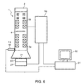
- Figure 6 represents another possible arrangement of one or more devices and a TEM according to the invention. Illustrated is a schematic drawing of a TEM 1 comprising an electron gun 2, deflector coils 53 located before the sample, the sample 4, deflector coils 54 located after the sample and a fluorescent screen 21.
- a single device 55 connected to the TEM 1, contains a coil pre-amplifier if necessary, an interface, a scan generator, precession signal generator, an preamplifier and analogue to digital converter for connection to the Faraday cage 23.
- Device 55 is connected to a computer 31, with a computer monitor 56.
- the computer has a computer readable media comprising an image of the software described in Figure 2 .
- a CCD camera 19 or diffractometer 18 mounted in a 35mm port connects to the computer 31 in this example, though it may equally well connect to the device 55, said device containing the necessary circuitry for transfer of data from the CCD camera 19 or diffractometer 18 to the computer 31.
Landscapes
- Chemical & Material Sciences (AREA)
- Analytical Chemistry (AREA)
- Crystallography & Structural Chemistry (AREA)
- Physics & Mathematics (AREA)
- Health & Medical Sciences (AREA)
- Life Sciences & Earth Sciences (AREA)
- Biochemistry (AREA)
- General Health & Medical Sciences (AREA)
- General Physics & Mathematics (AREA)
- Immunology (AREA)
- Pathology (AREA)
- Analysing Materials By The Use Of Radiation (AREA)
- Length-Measuring Devices Using Wave Or Particle Radiation (AREA)
Claims (21)
- Verfahren zum Messen von Elektronenbeugungsmustern (ED-Muster) einer Probe, wobei diese Muster dazu geeignet sind, um daraus unter Verwendung eines Transmissions-Elektronenmikroskops (1), TEM, eine Struktur zu bestimmen, wobei das ED-Muster durch Ablenkspulen (9) im TEM, die nach der Probe (4) gelegen sind, abgetastet wird, und wobei der Elektronenstrahl durch Ablenkspulen (6) im TEM (1), die vor der Probe gelegen sind, in Kombination mit einer ähnlichen Präzession des ED-Musters durch Ablenkspulen (9), die nach der Probe (4) gelegen sind, präzediert wird.
- Verfahren nach Anspruch 1, wobei die nach der Probe (4) gelegenen Spulen (9), um zum Abtasten des ED-Musters und zum Präzedieren des Elektronenstrahls die gleichen sind.
- Verfahren nach Anspruch 1 oder 2, ferner umfassend die folgenden Schritte vor der Messung der Intensitäten:a) Einwirkenlassen einer niedrigen Elektronenstrahldosis auf die Probe,b) schnelles Aufzeichnen eines ED-Musters unter Verwendung einer Kamera (19) mit ladungsgekoppeltem Bauelement, CCD, oder
schnelles Aufzeichnen eines ED-Musters unter Verwendung eines Diffraktometers (18) im schnellen Abtastmodus,c) Austasten des Strahls,d) Ableiten eines oder mehrerer Parameter aus dem in Schritt b) erhaltenen ED-Muster, die während der Messung der Intensitäten verwendet werden sollen,e) Aufheben des Austastens des Strahls, undf) Messen präziser Intensitäten unter Verwendung der in Schritt d) bestimmten Parameter. - Verfahren nach Anspruch 3, wobei es sich bei den Parametern von Schritt d) um einen oder mehrere der folgenden handelt:- die Anzahl der Stellen oder Bereiche des abzutastenden reziproken Raums,- die Anzahl der Abtaststufen,- die Stufengröße.
- Verfahren nach Anspruch 3, ferner umfassend einen Schritt des Bestimmens des Probenabbaus in der Probe, umfassend das Vergleichen der Intensität einer bestimmten Reflexion während der Messung der Intensitäten mit einer Bezugsreflexion, die durch das ED-Muster, das durch die CCD-Kamera (19) oder ein Diffraktometer (18) erfasst wurde, bestimmt wurde.
- Verfahren nach einem der Ansprüche 3 bis 5, ferner umfassend die folgenden Schritte:a) Vergleichen der Intensität einer bestimmten Reflexion, die während der Messung der Intensitäten gemessen wurde, mit einer Bezugsreflexion, die durch das ED-Muster, das durch das Diffraktometer (18) erfasst wurde, bestimmt wurde,b) Bestimmen des Probenabbaus und/oder der Strahlstabilität aus dem in Schritt a) vorgenommenen Vergleich, undc) Regulieren jeglicher Parameter während der Messung der Intensitäten und/oder Regulieren der Analyse nach der Messung der Intensitäten.
- Verfahren nach einem der Ansprüche 1 bis 5, ferner umfassend die folgenden Schritte:a) Messen des Elektronenstrahlstroms während der Messung der Intensitäten unter Verwendung einer isolierten Kondensatormembran, die sich auf dem Strahlweg befindet, bevor der Strahl mit der Probe in Kontakt tritt,b) Bestimmen der Strahlstabilität durch Überwachen des Stroms in Schritt a) im Lauf der Zeit, undc) Regulieren jeglicher Parameter während der Messung der Intensitäten und/oder Regulieren der Analyse nach der Messung der Intensitäten.
- Verfahren nach einem der Ansprüche 1 bis 7, wobei ein oder mehrere Faradaysche Käfige (23) verwendet werden, um die Reflexionen des ED-Musters während der Messung der Intensitäten zu messen.
- Verfahren nach Anspruch 8, ferner umfassend die folgenden Schritte:a) Zulassen, dass sich die Ladung von einem Faradayschen Käfig (23) an einem Vorverstärker (35), der wenige Femtoampere Ableitstrom aufweist, ansammelt; wobei die positive Ladung von transitiven Strömen den Verstärker einschaltet,b) Entladen des Faradayschen Käfigs (23) während der Messung der Intensitäten durch den Elektronenstrahl,c) Auflösen der Tätigkeit von Zählimpulsen unter Verwendung eines steuernden Vergleichers mit zwei Schwellenwerten, der von einem Quarzgenerator wirkt, während eines Messzyklus,d) Bestimmen der Ladung des Faradayschen Käfigs (23) aus dem Ausgang des Verstärkers (35),e) Bestimmen des Stroms eines Elektronenstrahls aus der Anzahl der Impulse, die im Zähler aufgezeichnet wurden.
- Verfahren nach einem der Ansprüche 1 bis 9, wobei eine Kombination aus einem Szintillator und einem Photovervielfacher verwendet wird, um das ED-Muster während der Messung der Intensitäten zu analysieren.
- Verfahren nach einem der Ansprüche 1 bis 9, wobei ein Continuous Dynode Electron Multiplier, CDEM, verwendet wird, um das ED-Muster während der Messung der Intensitäten zu analysieren.
- TEM-Anpassvorrichtung, umfassend einen Abtastgenerator (43) und einen Präzessionssignalgenerator (41), wobei der Abtastgenerator dazu konfiguriert ist, das ED-Muster durch Ablenkspulen im TEM, die nach der Probe (4) gelegen sind, abzutasten, und wobei der Präzessionssignalgenerator (41) dazu konfiguriert ist, den Elektronenstrahl durch Ablenkspulen (6) im TEM (1), die vor der Probe gelegen sind, in Kombination mit einer ähnlichen Präzession des ED-Musters durch Ablenkspulen (9), die nach der Probe (4) gelegen sind, zu präzedieren.
- Vorrichtung nach Anspruch 12, ferner umfassend einen Inverter und Adapter (42), der an den Ausgang des Signalpräzessionsgenerators (41) angeschlossen ist.
- Vorrichtung nach Anspruch 12 oder 13, ferner umfassend eine CCD-Kamera (19) und/oder ein Diffraktometer (18).
- Vorrichtung nach einem der Ansprüche 12 bis 14, ferner umfassend eine isolierte Kondensatormembran, die sich auf dem Strahlweg befindet, bevor der Strahl mit der Probe in Kontakt tritt.
- Vorrichtung nach einem der Ansprüche 12 bis 15, ferner umfassend einen oder mehrere Faradaysche Käfige (23), eine Kombination aus einem Szintillator und einem Photovervielfacher, und/oder ein CDEM, die jeweils ein Analog-Digital-Umwandlungsmittel aufweisen.
- Vorrichtung nach einem der Ansprüche 12 bis 16, ferner umfassend einen Computer (31) mit einem computerlesbaren Speichermittel, der mit einer oder mehreren der obigen Vorrichtungen verbunden ist.
- Vorrichtung nach einem der Ansprüche 12 bis 17, ferner umfassend eine Befestigung (22), die ermöglicht, dass ein oder mehrere Faradaysche Käfige, eine Kombination aus einem Szintillator und einem Photovervielfacher, und/oder ein CDEM an der Unterseite der TEM-Säule, und/oder im Anschluss für eine 35-mm-Kamera, und/oder in jedem beliebigen verfügbaren Anschluss angebracht werden.
- Vorrichtung nach einem der Ansprüche 12 bis 18, ferner umfassend einen Vorverstärker (23) aus einem Faradayschen Käfig, der eine Stromableitung zwischen 1 und 50 Femtoampere aufweist.
- Verwendung einer Vorrichtung nach einem der Ansprüche 12 bis 19, um ED-Muster einer Probe zu messen, wobei diese Muster dazu geeignet sind, um daraus unter Verwendung eines Transmissions-Elektronenmikroskops eine Struktur zu bestimmen.
- TEM (1), umfassend eine Vorrichtung nach einem der Ansprüche 12 bis 20.
Applications Claiming Priority (1)
| Application Number | Priority Date | Filing Date | Title |
|---|---|---|---|
| PCT/EP2003/009727 WO2005022582A1 (en) | 2003-09-02 | 2003-09-02 | A method for measuring diffraction patterns from a transmission electron microscopy to determine crystal structures and a device therefor |
Publications (2)
| Publication Number | Publication Date |
|---|---|
| EP1665321A1 EP1665321A1 (de) | 2006-06-07 |
| EP1665321B1 true EP1665321B1 (de) | 2009-11-11 |
Family
ID=34259108
Family Applications (1)
| Application Number | Title | Priority Date | Filing Date |
|---|---|---|---|
| EP03750478A Expired - Lifetime EP1665321B1 (de) | 2003-09-02 | 2003-09-02 | Verfahren zur messung der beugungsmuster mit hilfe eines transmissionselektronenmikrosops zur ermittlung der kristallstruktur und vorrichtung hierfür |
Country Status (6)
| Country | Link |
|---|---|
| US (1) | US7601956B2 (de) |
| EP (1) | EP1665321B1 (de) |
| AT (1) | ATE448561T1 (de) |
| AU (1) | AU2003270138A1 (de) |
| DE (1) | DE60330067D1 (de) |
| WO (1) | WO2005022582A1 (de) |
Cited By (1)
| Publication number | Priority date | Publication date | Assignee | Title |
|---|---|---|---|---|
| EP2642279A1 (de) | 2012-03-19 | 2013-09-25 | Universidad de Barcelona | Verfahren und System zur Verbesserung von kennzeichnenden Spitzensignalen bei der analytischen Elektronenmikroskopie |
Families Citing this family (18)
| Publication number | Priority date | Publication date | Assignee | Title |
|---|---|---|---|---|
| US7531812B2 (en) * | 2003-10-27 | 2009-05-12 | Politechnika Wroclawska | Method and system for the directional detection of electrons in a scanning electron microscope |
| JP2006079911A (ja) * | 2004-09-09 | 2006-03-23 | Hitachi High-Technologies Corp | 電子ビーム電流計測方法、電子ビーム描画装置および電子ビーム検出器 |
| DE102006011615A1 (de) | 2006-03-14 | 2007-09-20 | Carl Zeiss Nts Gmbh | Phasenkontrast-Elektronenmikroskop |
| WO2008060237A1 (en) * | 2006-11-15 | 2008-05-22 | Hovmoeller Sven | Electron rotation camera |
| US7700915B2 (en) * | 2006-11-28 | 2010-04-20 | Canatu Oy | Method, computer program and apparatus for the characterization of molecules |
| US7952073B2 (en) * | 2008-08-01 | 2011-05-31 | Direct Electron, Lp | Apparatus and method including a direct bombardment detector and a secondary detector for use in electron microscopy |
| JP5536085B2 (ja) * | 2008-11-06 | 2014-07-02 | ナノメガス エスピーアールエル | 電子線回折による高スループット結晶構造解析のための方法及びデバイス |
| US8748817B2 (en) * | 2010-07-27 | 2014-06-10 | Vineet Kumar | Orientation imaging using wide angle convergent beam diffraction in transmission electron microscopy |
| EP2413345B1 (de) | 2010-07-29 | 2013-02-20 | Carl Zeiss NTS GmbH | Strahlensystem mit geladenen Teilchen |
| KR101999988B1 (ko) * | 2012-03-08 | 2019-07-15 | 앱파이브 엘엘씨 | 고 공간 분해능에서 물질의 스트레인을 측정하기 위한 시스템 및 공정 |
| US9244025B2 (en) * | 2013-07-05 | 2016-01-26 | Semiconductor Energy Laboratory Co., Ltd. | Transmission electron diffraction measurement apparatus and method for measuring transmission electron diffraction pattern |
| JP2015185511A (ja) * | 2014-03-26 | 2015-10-22 | 日本電子株式会社 | 荷電粒子線装置 |
| US9978557B2 (en) | 2016-04-21 | 2018-05-22 | Fei Company | System for orienting a sample using a diffraction pattern |
| EP3379236B1 (de) * | 2017-03-20 | 2019-09-11 | TESCAN Brno, s.r.o. | Rastertransmission-elektronenmikroskop |
| EP3379557A1 (de) * | 2017-03-20 | 2018-09-26 | TESCAN Brno, s.r.o. | Raster-transmissionselektronenmikroskop und verfahren zur erfassung mit hohem durchsatz von elektronenstreuungswinkelverteilungsbildern |
| JP7074479B2 (ja) * | 2018-01-11 | 2022-05-24 | 株式会社ニューフレアテクノロジー | マルチビーム検査装置 |
| US12072304B2 (en) | 2019-02-07 | 2024-08-27 | R. J. Dwayne Miller | Systems and methods for performing serial electron diffraction nanocrystallography |
| KR102724079B1 (ko) | 2019-05-20 | 2024-10-29 | 엘디코 사이언티픽 아게 | 하전 입자 결정학을 위한 회절계 |
Family Cites Families (7)
| Publication number | Priority date | Publication date | Assignee | Title |
|---|---|---|---|---|
| JPS5138578B2 (de) | 1972-10-23 | 1976-10-22 | ||
| US4697080A (en) * | 1986-01-06 | 1987-09-29 | The United States Of America As Represented By The United States Department Of Energy | Analysis with electron microscope of multielement samples using pure element standards |
| US6420701B1 (en) | 1997-07-23 | 2002-07-16 | Canon Kabushiki Kaisha | Method of determining average crystallite size of material and apparatus and method for preparing thin film of the material |
| JP2000243338A (ja) * | 1999-02-22 | 2000-09-08 | Hitachi Ltd | 透過電子顕微鏡装置および透過電子検査装置並びに検査方法 |
| EP1365229B1 (de) * | 2001-02-28 | 2012-12-12 | Hitachi, Ltd. | Elektronen-Nano-Diffraktionsmethode zur Messung von Dehnung und Spannung durch Detektion eines Diffraktionspunktes oder mehrerer Diffraktionspunkte |
| JP3867524B2 (ja) * | 2001-07-05 | 2007-01-10 | 株式会社日立製作所 | 電子線を用いた観察装置及び観察方法 |
| JP3789104B2 (ja) * | 2002-05-13 | 2006-06-21 | 株式会社日立ハイテクノロジーズ | 元素分布観察方法及び装置 |
-
2003
- 2003-09-02 WO PCT/EP2003/009727 patent/WO2005022582A1/en not_active Ceased
- 2003-09-02 AU AU2003270138A patent/AU2003270138A1/en not_active Abandoned
- 2003-09-02 US US10/570,336 patent/US7601956B2/en not_active Expired - Fee Related
- 2003-09-02 AT AT03750478T patent/ATE448561T1/de not_active IP Right Cessation
- 2003-09-02 EP EP03750478A patent/EP1665321B1/de not_active Expired - Lifetime
- 2003-09-02 DE DE60330067T patent/DE60330067D1/de not_active Expired - Lifetime
Cited By (2)
| Publication number | Priority date | Publication date | Assignee | Title |
|---|---|---|---|---|
| EP2642279A1 (de) | 2012-03-19 | 2013-09-25 | Universidad de Barcelona | Verfahren und System zur Verbesserung von kennzeichnenden Spitzensignalen bei der analytischen Elektronenmikroskopie |
| US9406496B2 (en) | 2012-03-19 | 2016-08-02 | Universitat De Barcelona | Method and system for improving characteristic peak signals in analytical electron microscopy |
Also Published As
| Publication number | Publication date |
|---|---|
| US20070023659A1 (en) | 2007-02-01 |
| EP1665321A1 (de) | 2006-06-07 |
| DE60330067D1 (de) | 2009-12-24 |
| ATE448561T1 (de) | 2009-11-15 |
| US7601956B2 (en) | 2009-10-13 |
| WO2005022582A1 (en) | 2005-03-10 |
| AU2003270138A1 (en) | 2005-03-16 |
Similar Documents
| Publication | Publication Date | Title |
|---|---|---|
| EP1665321B1 (de) | Verfahren zur messung der beugungsmuster mit hilfe eines transmissionselektronenmikrosops zur ermittlung der kristallstruktur und vorrichtung hierfür | |
| Koster et al. | Automated microscopy for electron tomography | |
| Dierksen et al. | Towards automatic electron tomography | |
| Hammersley et al. | Two-dimensional detector software: from real detector to idealised image or two-theta scan | |
| Krivanek et al. | Applications of slow-scan CCD cameras in transmission electron microscopy | |
| Mastronarde | Automated electron microscope tomography using robust prediction of specimen movements | |
| EP2530699B1 (de) | Ladungsträgerstrahl-mikroskop und messverfahren damit | |
| US6051834A (en) | Electron microscope | |
| Sakabe et al. | Weissenberg camera for macromolecules with imaging plate data collection system at the Photon Factory: Present status and future plan | |
| JP7105647B2 (ja) | 透過型荷電粒子顕微鏡における回折パターン検出 | |
| US6548811B1 (en) | Transmission electron microscope apparatus with equipment for inspecting defects in specimen and method of inspecting defects in specimen using transmission electron microscope | |
| JP2003014667A (ja) | 電子線を用いた観察装置及び観察方法 | |
| Sherman et al. | Performance of a slow-scan CCD camera for macromolecular imaging in a 400 kV electron cryomicroscope | |
| Grimm et al. | Zero‐loss energy filtering under low‐dose conditions using a post‐column energy filter | |
| EP4067886A1 (de) | Verfahren und system zur bestimmung einer kristallstruktur | |
| JPH09167591A (ja) | 走査透過電子顕微鏡 | |
| Schmid et al. | ViPErLEED package II: Spot tracking, extraction, and processing of I (V) curves | |
| Prutton et al. | Scanning Auger electron microscopy with high spatial or high energy resolution | |
| Vulovic et al. | A toolkit for the characterization of CCD cameras for transmission electron microscopy | |
| EP3637452A1 (de) | Ladungsträgerteilchenmikroskop und verfahren zur anpassung eines ladungsträgerteilchenmikroskops | |
| JP2002139464A (ja) | 半導体装置の検査方法および検査装置 | |
| Typke et al. | High-throughput film-densitometry: an efficient approach to generate large data sets | |
| Kulygin et al. | New approaches to precise measurements of electron diffraction patterns | |
| CN118937330A (zh) | 一种基于光电联合的晶圆检测装置及方法 | |
| US3229087A (en) | Electron microanalyzer and monitoring system |
Legal Events
| Date | Code | Title | Description |
|---|---|---|---|
| PUAI | Public reference made under article 153(3) epc to a published international application that has entered the european phase |
Free format text: ORIGINAL CODE: 0009012 |
|
| 17P | Request for examination filed |
Effective date: 20060403 |
|
| AK | Designated contracting states |
Kind code of ref document: A1 Designated state(s): AT BE BG CH CY CZ DE DK EE ES FI FR GB GR HU IE IT LI LU MC NL PT RO SE SI SK TR |
|
| DAX | Request for extension of the european patent (deleted) | ||
| 17Q | First examination report despatched |
Effective date: 20080317 |
|
| GRAP | Despatch of communication of intention to grant a patent |
Free format text: ORIGINAL CODE: EPIDOSNIGR1 |
|
| GRAS | Grant fee paid |
Free format text: ORIGINAL CODE: EPIDOSNIGR3 |
|
| GRAA | (expected) grant |
Free format text: ORIGINAL CODE: 0009210 |
|
| AK | Designated contracting states |
Kind code of ref document: B1 Designated state(s): AT BE BG CH CY CZ DE DK EE ES FI FR GB GR HU IE IT LI LU MC NL PT RO SE SI SK TR |
|
| REG | Reference to a national code |
Ref country code: GB Ref legal event code: FG4D |
|
| REG | Reference to a national code |
Ref country code: CH Ref legal event code: EP |
|
| REG | Reference to a national code |
Ref country code: IE Ref legal event code: FG4D |
|
| REF | Corresponds to: |
Ref document number: 60330067 Country of ref document: DE Date of ref document: 20091224 Kind code of ref document: P |
|
| NLV1 | Nl: lapsed or annulled due to failure to fulfill the requirements of art. 29p and 29m of the patents act | ||
| PG25 | Lapsed in a contracting state [announced via postgrant information from national office to epo] |
Ref country code: SE Free format text: LAPSE BECAUSE OF FAILURE TO SUBMIT A TRANSLATION OF THE DESCRIPTION OR TO PAY THE FEE WITHIN THE PRESCRIBED TIME-LIMIT Effective date: 20091111 Ref country code: PT Free format text: LAPSE BECAUSE OF FAILURE TO SUBMIT A TRANSLATION OF THE DESCRIPTION OR TO PAY THE FEE WITHIN THE PRESCRIBED TIME-LIMIT Effective date: 20100311 Ref country code: ES Free format text: LAPSE BECAUSE OF FAILURE TO SUBMIT A TRANSLATION OF THE DESCRIPTION OR TO PAY THE FEE WITHIN THE PRESCRIBED TIME-LIMIT Effective date: 20100222 Ref country code: FI Free format text: LAPSE BECAUSE OF FAILURE TO SUBMIT A TRANSLATION OF THE DESCRIPTION OR TO PAY THE FEE WITHIN THE PRESCRIBED TIME-LIMIT Effective date: 20091111 |
|
| PG25 | Lapsed in a contracting state [announced via postgrant information from national office to epo] |
Ref country code: CY Free format text: LAPSE BECAUSE OF FAILURE TO SUBMIT A TRANSLATION OF THE DESCRIPTION OR TO PAY THE FEE WITHIN THE PRESCRIBED TIME-LIMIT Effective date: 20091111 Ref country code: SI Free format text: LAPSE BECAUSE OF FAILURE TO SUBMIT A TRANSLATION OF THE DESCRIPTION OR TO PAY THE FEE WITHIN THE PRESCRIBED TIME-LIMIT Effective date: 20091111 |
|
| PG25 | Lapsed in a contracting state [announced via postgrant information from national office to epo] |
Ref country code: AT Free format text: LAPSE BECAUSE OF FAILURE TO SUBMIT A TRANSLATION OF THE DESCRIPTION OR TO PAY THE FEE WITHIN THE PRESCRIBED TIME-LIMIT Effective date: 20091111 Ref country code: BE Free format text: LAPSE BECAUSE OF FAILURE TO SUBMIT A TRANSLATION OF THE DESCRIPTION OR TO PAY THE FEE WITHIN THE PRESCRIBED TIME-LIMIT Effective date: 20091111 |
|
| PG25 | Lapsed in a contracting state [announced via postgrant information from national office to epo] |
Ref country code: EE Free format text: LAPSE BECAUSE OF FAILURE TO SUBMIT A TRANSLATION OF THE DESCRIPTION OR TO PAY THE FEE WITHIN THE PRESCRIBED TIME-LIMIT Effective date: 20091111 Ref country code: RO Free format text: LAPSE BECAUSE OF FAILURE TO SUBMIT A TRANSLATION OF THE DESCRIPTION OR TO PAY THE FEE WITHIN THE PRESCRIBED TIME-LIMIT Effective date: 20091111 Ref country code: BG Free format text: LAPSE BECAUSE OF FAILURE TO SUBMIT A TRANSLATION OF THE DESCRIPTION OR TO PAY THE FEE WITHIN THE PRESCRIBED TIME-LIMIT Effective date: 20100211 Ref country code: DK Free format text: LAPSE BECAUSE OF FAILURE TO SUBMIT A TRANSLATION OF THE DESCRIPTION OR TO PAY THE FEE WITHIN THE PRESCRIBED TIME-LIMIT Effective date: 20091111 |
|
| PG25 | Lapsed in a contracting state [announced via postgrant information from national office to epo] |
Ref country code: SK Free format text: LAPSE BECAUSE OF FAILURE TO SUBMIT A TRANSLATION OF THE DESCRIPTION OR TO PAY THE FEE WITHIN THE PRESCRIBED TIME-LIMIT Effective date: 20091111 Ref country code: CZ Free format text: LAPSE BECAUSE OF FAILURE TO SUBMIT A TRANSLATION OF THE DESCRIPTION OR TO PAY THE FEE WITHIN THE PRESCRIBED TIME-LIMIT Effective date: 20091111 |
|
| PLBE | No opposition filed within time limit |
Free format text: ORIGINAL CODE: 0009261 |
|
| STAA | Information on the status of an ep patent application or granted ep patent |
Free format text: STATUS: NO OPPOSITION FILED WITHIN TIME LIMIT |
|
| 26N | No opposition filed |
Effective date: 20100812 |
|
| PG25 | Lapsed in a contracting state [announced via postgrant information from national office to epo] |
Ref country code: GR Free format text: LAPSE BECAUSE OF FAILURE TO SUBMIT A TRANSLATION OF THE DESCRIPTION OR TO PAY THE FEE WITHIN THE PRESCRIBED TIME-LIMIT Effective date: 20100212 |
|
| PG25 | Lapsed in a contracting state [announced via postgrant information from national office to epo] |
Ref country code: IT Free format text: LAPSE BECAUSE OF FAILURE TO SUBMIT A TRANSLATION OF THE DESCRIPTION OR TO PAY THE FEE WITHIN THE PRESCRIBED TIME-LIMIT Effective date: 20091111 |
|
| PG25 | Lapsed in a contracting state [announced via postgrant information from national office to epo] |
Ref country code: MC Free format text: LAPSE BECAUSE OF NON-PAYMENT OF DUE FEES Effective date: 20100930 |
|
| REG | Reference to a national code |
Ref country code: CH Ref legal event code: PL |
|
| PG25 | Lapsed in a contracting state [announced via postgrant information from national office to epo] |
Ref country code: LI Free format text: LAPSE BECAUSE OF NON-PAYMENT OF DUE FEES Effective date: 20100930 Ref country code: CH Free format text: LAPSE BECAUSE OF NON-PAYMENT OF DUE FEES Effective date: 20100930 Ref country code: IE Free format text: LAPSE BECAUSE OF NON-PAYMENT OF DUE FEES Effective date: 20100902 |
|
| PG25 | Lapsed in a contracting state [announced via postgrant information from national office to epo] |
Ref country code: LU Free format text: LAPSE BECAUSE OF NON-PAYMENT OF DUE FEES Effective date: 20100902 Ref country code: HU Free format text: LAPSE BECAUSE OF FAILURE TO SUBMIT A TRANSLATION OF THE DESCRIPTION OR TO PAY THE FEE WITHIN THE PRESCRIBED TIME-LIMIT Effective date: 20100512 Ref country code: NL Free format text: LAPSE BECAUSE OF FAILURE TO SUBMIT A TRANSLATION OF THE DESCRIPTION OR TO PAY THE FEE WITHIN THE PRESCRIBED TIME-LIMIT Effective date: 20091111 |
|
| PG25 | Lapsed in a contracting state [announced via postgrant information from national office to epo] |
Ref country code: TR Free format text: LAPSE BECAUSE OF FAILURE TO SUBMIT A TRANSLATION OF THE DESCRIPTION OR TO PAY THE FEE WITHIN THE PRESCRIBED TIME-LIMIT Effective date: 20091111 |
|
| PGFP | Annual fee paid to national office [announced via postgrant information from national office to epo] |
Ref country code: DE Payment date: 20140922 Year of fee payment: 12 |
|
| PGFP | Annual fee paid to national office [announced via postgrant information from national office to epo] |
Ref country code: GB Payment date: 20140919 Year of fee payment: 12 Ref country code: FR Payment date: 20140919 Year of fee payment: 12 |
|
| REG | Reference to a national code |
Ref country code: DE Ref legal event code: R119 Ref document number: 60330067 Country of ref document: DE |
|
| GBPC | Gb: european patent ceased through non-payment of renewal fee |
Effective date: 20150902 |
|
| REG | Reference to a national code |
Ref country code: FR Ref legal event code: ST Effective date: 20160531 |
|
| PG25 | Lapsed in a contracting state [announced via postgrant information from national office to epo] |
Ref country code: GB Free format text: LAPSE BECAUSE OF NON-PAYMENT OF DUE FEES Effective date: 20150902 Ref country code: DE Free format text: LAPSE BECAUSE OF NON-PAYMENT OF DUE FEES Effective date: 20160401 |
|
| PG25 | Lapsed in a contracting state [announced via postgrant information from national office to epo] |
Ref country code: FR Free format text: LAPSE BECAUSE OF NON-PAYMENT OF DUE FEES Effective date: 20150930 |