EP1666954A1 - Modulateur optique - Google Patents
Modulateur optique Download PDFInfo
- Publication number
- EP1666954A1 EP1666954A1 EP04772548A EP04772548A EP1666954A1 EP 1666954 A1 EP1666954 A1 EP 1666954A1 EP 04772548 A EP04772548 A EP 04772548A EP 04772548 A EP04772548 A EP 04772548A EP 1666954 A1 EP1666954 A1 EP 1666954A1
- Authority
- EP
- European Patent Office
- Prior art keywords
- electrode
- branched
- substrate
- electrodes
- ground
- Prior art date
- Legal status (The legal status is an assumption and is not a legal conclusion. Google has not performed a legal analysis and makes no representation as to the accuracy of the status listed.)
- Withdrawn
Links
Images



Classifications
-
- G—PHYSICS
- G02—OPTICS
- G02F—OPTICAL DEVICES OR ARRANGEMENTS FOR THE CONTROL OF LIGHT BY MODIFICATION OF THE OPTICAL PROPERTIES OF THE MEDIA OF THE ELEMENTS INVOLVED THEREIN; NON-LINEAR OPTICS; FREQUENCY-CHANGING OF LIGHT; OPTICAL LOGIC ELEMENTS; OPTICAL ANALOGUE/DIGITAL CONVERTERS
- G02F1/00—Devices or arrangements for the control of the intensity, colour, phase, polarisation or direction of light arriving from an independent light source, e.g. switching, gating or modulating; Non-linear optics
- G02F1/01—Devices or arrangements for the control of the intensity, colour, phase, polarisation or direction of light arriving from an independent light source, e.g. switching, gating or modulating; Non-linear optics for the control of the intensity, phase, polarisation or colour
- G02F1/21—Devices or arrangements for the control of the intensity, colour, phase, polarisation or direction of light arriving from an independent light source, e.g. switching, gating or modulating; Non-linear optics for the control of the intensity, phase, polarisation or colour by interference
- G02F1/225—Devices or arrangements for the control of the intensity, colour, phase, polarisation or direction of light arriving from an independent light source, e.g. switching, gating or modulating; Non-linear optics for the control of the intensity, phase, polarisation or colour by interference in an optical waveguide structure
- G02F1/2255—Devices or arrangements for the control of the intensity, colour, phase, polarisation or direction of light arriving from an independent light source, e.g. switching, gating or modulating; Non-linear optics for the control of the intensity, phase, polarisation or colour by interference in an optical waveguide structure controlled by a high-frequency electromagnetic component in an electric waveguide structure
-
- G—PHYSICS
- G02—OPTICS
- G02F—OPTICAL DEVICES OR ARRANGEMENTS FOR THE CONTROL OF LIGHT BY MODIFICATION OF THE OPTICAL PROPERTIES OF THE MEDIA OF THE ELEMENTS INVOLVED THEREIN; NON-LINEAR OPTICS; FREQUENCY-CHANGING OF LIGHT; OPTICAL LOGIC ELEMENTS; OPTICAL ANALOGUE/DIGITAL CONVERTERS
- G02F2203/00—Function characteristic
- G02F2203/25—Frequency chirping of an optical modulator; Arrangements or methods for the pre-set or tuning thereof
Definitions
- the present invention relates to an optical modulator.
- a CPW (coplanar type) electrode pattern and Mach-Zehnder type optical waveguide are formed on an X-cut lithium niobate.
- the applied electric fields onto branched parts of the optical waveguide as well as the lengths of the interacting parts with electrodes are adjusted to be the same, so as to obtain an optical modulator of zero chirp property.
- a predetermined chirp amount is advantageously imparted even for an optical modulator using an X-cut or Y-cut as a substrate. It has not been, however, studied to impart such predetermined chirp amount onto an optical modulator using the X-cut or Y-cut made of an electro-optic crystal.
- An object of the present invention is to provide an optical modulator having a substrate comprising an electro-optic material and first and second main faces, an optical waveguide formed on the substrate and having first and second branched parts, and ground and signal electrodes provided on the side of the first main face of the substrate, whose chirp amount can be controlled at an appropriate value.
- the present invention provides an optical modulator comprising a substrate comprising an electro-optic material and first and second main faces, an optical waveguide formed on the substrate and having first and second branched parts, and ground and signal electrodes provided on the side of the first main face of the substrate.
- the first branched part and second branched part are provided in an electrode gap defined between the ground and signal electrodes.
- Microwave electric fields are applied onto interacting parts with electrodes of the first and second branched parts, respectively, to modulate light propagating in the first and second branched parts. Integral values of field intensities over interaction lengths with electrodes in the first and second branched parts are different from each other so that a predetermined chirp amount is obtained.
- the present invention further provides an optical modulator comprising a substrate comprising an electro-optic material and first and second main faces, an optical waveguide formed on the substrate and having first and second branched parts, and ground and signal electrodes provided on the side of the first main face of the substrate.
- the first branched part is provided in an electrode gap defined between the ground and signal electrodes.
- the second branched part is provided under the ground electrode. Microwave electric fields are applied onto interacting parts with electrodes of the first and second branched parts, respectively, to modulate light propagating in the first and second branched parts, respectively.
- Respective integral values A 1 and A 2 of electric field intensities Ex(z) by interaction lengths with electrodes "z” are calculated for two branched parts (optical waveguides) "a” and “b", respectively, of an optical modulator.
- the interaction length with electrode of the electric field intensities of the branched part means a value obtained by integrating the electric fields Ex(z) at the respective points "z" of the branched part over the whole length "L” of the branched part.
- the integral value is given as follows. ⁇ 0 L E x ( z ) d z
- ⁇ n 1 and ⁇ n 2 represent changes of refractive indices in the waveguides "a" and "b". The average change of refractive index is proportional to the following. ⁇ 0 L E x ( z ) d z
- the respective integral values of the electric field intensities over the interaction lengths with electrodes in the first and second branched parts are made different from each other.
- the optical modulator is thus adjusted so that a predetermined chirp amount is obtained.
- microwave electric field is applied to each of first and second branched parts so that the intensities of the electric fields are different from each other.
- the integral values of the electric field intensities over the interaction length with electrode are made different from each other. Specific examples for this are not particularly limited.
- plurality of ground electrodes is provided so that the widths of the electrode gaps of the signal and ground electrodes are made different from each other.
- Fig. 1 is a cross sectional view schematically showing an optical modulator 1A according to this embodiment.
- the optical modulator 1A has a substrate 2, for example, of a shape of a flat plate. Branched parts 3 and 5 are provided on the side of a first main face 2a of the substrate 2. Further, a signal electrode 4B and ground electrodes 4A and 4C of, for example, coplanar type is provided on the main face 2a.
- the branched part 3 is positioned in an electrode gap 20A and the branched part 5 is positioned in an electrode gap 20B.
- electrode configuration of so called Coplanar waveguide (CPW electrode) is applied according to the present example, the configuration of electrodes is not particularly limited.
- the present invention may be applied to electrode configuration of so-called ACPS type (Asymmetric coplanar strip-line type).
- the branched parts 3 and 5 are formed between the ground electrode 4A and center electrode 4B and between the center electrode 4B and ground electrode 4C, respectively, so that signal voltages are applied onto the branched parts 3 and 5, respectively, substantially in horizontal direction.
- the optical waveguide constitutes an optical waveguide of so-called Mach-Zehnder type.
- the electric field intensity applied onto the branched part 5 is relatively large in the narrower electrode gap 20A, so that the integral value of the field intensity over the interaction length with electrode becomes larger.
- the electric field intensity applied onto the branched part 5 is smaller in the wider electrode gap 20B. It is thus possible to adjust the chirp amount of the optical modulator 1A at a desired value.
- a difference of G 1 and G 2 may preferably be 3 micrometer or larger, and more preferably be 20 micrometer or larger.
- G 1 may preferably be 100 micrometer or smaller and more preferably be 40 micrometer or smaller, for reducing the overall V ⁇ L.
- G 1 and G 2 may preferably be 1 micrometer or larger and more preferably 3 micrometer or larger, for preventing the conduction of the signal and ground electrodes.
- G 1 was set at 20 ⁇ m.
- the width of the signal electrode 4B was set at 30 ⁇ m, the substrate 2 was made of lithium niobate single crystal, and the thickness Tsub was made 8 ⁇ m.
- the thickness Tm of the electrode was made 26 ⁇ m.
- G 2 of the wider electrode gap 20B is variously changed in a range of 30 to 100 ⁇ m as shown in table 1.
- the impedance Zc, the overall V ⁇ L, V ⁇ L1 of the branched part 3, V ⁇ L2 of the branched part 5, and chirp amount ( ⁇ -para) were calculated. The results were shown in table 1.
- the chirp amount ⁇ of the optical modulator can be appropriately controlled in a wide range by changing the width G2 of the electrode gap 20B.
- the first branched part is positioned in the proximity of the edge of the signal or ground electrode in the narrower electrode gap.
- the branched part 3 is positioned in the proximity of an edge "E" of the signal electrode 4B or edge “E” of the ground electrode 4A in the narrower electrode gap 20A.
- a relatively higher electric field is applied onto the branched part 3 on the side of the narrower electrode gap 20A.
- the branched part 3a is positioned in the proximity of the edge "E" of the signal electrode 4B or the edge "E” of the ground electrode 4A, so as to improve the field intensity applied on the branched part 3a.
- the chirp amount can be thus adjusted in a larger range and the product V ⁇ L of driving voltage and electrode length can be lowered.
- a distance d1 of the central line "S" of the branched part 3 and the signal electrode or ground electrode may preferably be 20 micrometer or smaller, and more preferably be 10 micrometer or smaller.
- the distance of the branched part 5 and the ground or signal electrode may preferably be larger in the wider electrode gap 20B, for further elevating the chirp amount of an optical waveguide. It is thus possible to minimize the electric field intensity applied on the branched part 5 and elevate the chirp amount of the optical modulator.
- the distance d2 (smaller one) of the branched part and the ground or signal electrode may preferably be 10 micrometer or larger and more preferably be 20 micrometer or larger.
- the first and second branched parts have interaction lengths with electrodes different from each other. It is thus possible that the integral values of electric field intensities over the interaction lengths with electrodes can be made different from each other. This is because the larger the interaction length "L" with electrode, the larger the integral value, provided that the field intensity is substantially the same.
- a part of the first branched part is positioned under the signal or ground electrode so that the interaction length with electrode of the first branched part can be made shorter that that of the second branched part.
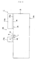
- Fig. 3 is a plan view schematically showing an optical modulator 1C according to this embodiment.
- Mach-Zehnder type optical waveguides 6, 7, 3 and 5 are provided on a substrate 2.
- the second branched part 3 is formed in an electrode gap 20A of a signal electrode 4B and a ground electrode 4A, so that a uniform electric field Ex is applied over the whole length "L" (substantially L1 + L2).
- electric field of substantially uniform intensity is applied over the whole length of a part 5a in an electrode gap 20B of the first branched part 5. Further, an electric field is applied to an inclined part 5b.
- the widths of the electrode gaps may be made different from each other, or the distances of the branched parts and the electrode edges may be made different from each other. It is thus possible to control the chirp amount of the optical modulator in a still wider range.
- a plurality of ground electrodes are provided. Moreover, the thickness of a substrate under an electrode gap of a signal electrode and a first ground electrode and the thickness of the substrate under an electrode gap of the signal electrode and a second ground electrode are made different from each other. The electric field intensity applied on the branched part in the electrode gap on the side of the thicker region of the substrate is different from that on the side of the thinner region of the substrate. It is thus possible that the integral values can be made different from each other.
- Fig. 4 is a cross sectional view schematically showing an optical modulator 1D according to this embodiment. Structural parts and dimensions already shown in Fig. 1 are depicted using the same numerals and the description is referred to.
- a substrate 12 has a thicker part 12c having a larger thickness and a thinner part 12d having a smaller thickness. 12a and 12b represent the main faces.
- An electrode gap 20A is provided on the side of the thinner part 12d and the electrode gap 20B is provided on the side of the thicker part 12c.
- a difference of the thickness Tsub1 of the thinner part 12d and the thickness Tsub 2 of the thicker part 12c may preferably be 2 micrometer or more and more preferably be 20 micrometer or more, for obtaining different integral values for the branched parts 3 and 5. Further, on the viewpoint of high speed modulation, Tsub1 may preferably be 20 micrometer or lower.
- a plurality of ground electrodes is provided.
- a first low dielectric part is provided under a substrate and under an electrode gap between a signal electrode and a first ground electrode
- a second low dielectric part is provided under the substrate and under an electrode gap between the signal electrode and a second ground electrode.
- the dielectric constant of the first low dielectric part is made different from that of the second low dielectric part.
- Fig. 5 is a cross sectional view schematically showing an optical waveguide 1E according to this embodiment. Structural parts and dimensions already shown in Fig. 1 are depicted using the same numerals and the description is referred to.
- a first low dielectric part 10A and a second low dielectric part 10B are provided under the substrate 2.
- An electrode gap 20A is provided on the side of the low dielectric part 10A, and an electrode gap 20B is provided on the side of the low dielectric part 20B.
- the ratio of the dielectric constant of the low dielectric part 10A and that of the low dielectric part 10B may preferably be 2 times or larger, and more preferably be 5 times or larger.
- a first branched part is provided in an electrode gap between a ground electrode and a signal electrode, and a second branched part is provided under a ground electrode.
- Microwave electric field is applied on each of the interacting parts with electrode of the first and second branched parts to modulate light propagating the first and second branched parts, respectively.
- the first branched part is positioned in the electrode gap so that the chirp amount can be appropriately adjusted.
- the electric field strengths applied onto the two branched parts are different from each other, so that the chirp amount ( ⁇ -para) is typically about 0.6 to 0.7.
- the chirp amount can be adjusted at an appropriate value for an applied system.
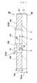
- Fig. 6 is a cross sectional view schematically showing an optical modulator 11 according to this embodiment.
- a first branched part 14 and a second branched part 15 of Mach-Zehnder type optical waveguide are formed on the main face 13a of a substrate 13.
- 13b represents a bottom face of the substrate 13.
- the branched part 15 is provided under a signal electrode 17B with a buffer layer 16 interposed between them.
- An electrode gap 25 is provided between a signal electrode 17A and a ground electrode 17B.
- the branched part 14 is extended into the electrode gap 25, and the central line "S" of the branched part 14 is provided outside of the edge "E" of the signal electrode 17A by a distance of "t".
- the branched part 14 and signal electrode 17A are separated with the buffer layer 16.
- an electric field may preferably be applied on each branched part in the direction substantially perpendicular to the main face of the substrate.
- the thickness of the substrate is 30 ⁇ m or smaller at least in a region of interaction length with electrode.
- the substrate has a base part having a thickness of 30 ⁇ m or larger, preferably 200 ⁇ m or larger, and a recess is formed inside of the base part. According to such substrate, it is possible to realize high speed modulation while imparting a mechanical strength suitable to handling.
- the substrate has a first thinner part having a relatively larger thickness and facing the recess and a second thinner part having a smaller thickness and facing the recess, and the optical waveguide is provided in the first thinner part.
- This type of substrate may be comprised of main bodies described in Japanese patent publication 10-133159A and 2002-169133A.
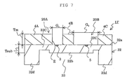
- a substrate 32 shown in Fig. 7 has a base part 32d, a first thinner part 32b facing a recess 33 and having a relatively larger thickness and a second thinner part 32c facing the recess 33 and having a smaller thickness.
- the optical waveguide is provided in the first thinner part 32b.
- 32a represents a main face of the substrate.
- the bottom faces of the substrates 2, 12 and 13 may be joined with a separate supporting body through a joining layer.
- the material forming the optical waveguide substrates 2, 12 and 13 are made of a ferroelectric electro-optic material and may preferably of a single crystal. Although such crystal is not particularly limited as far as the modulation of light is possible, the crystal includes lithium niobate, lithium tantalite, a solid solution of lithium niobate-lithium tantalite, potassium lithium niobate, KTP, GaAs and quartz.
- the materials of the ground and signal electrodes are not particularly limited as far as the material has a low resistance and is excellent in impedance characteristic, and may be composed of gold, silver, copper or the like.
- the buffer layer may be made of known materials such as silicon oxide, magnesium fluoride, silicon nitride and alumina.
- the optical waveguides are provided in the main body and preferably on the side of the first main face of the main body.
- the optical waveguide may be a ridge type optical waveguide directly formed on the first main face of the main body, or a ridge type optical waveguide formed on another layer on the first main face of the main body, or an optical waveguide formed by inner diffusion or ion exchange process inside of the main body, such as titanium diffusion or proton exchange optical waveguide.
- the electrodes are provided on the side of the first main face of the main body. The electrodes may be formed directly on the first main face of the main body, or may be formed on a buffer layer.
- low dielectric part means a part having a dielectric constant lower than that of the electro-optic material forming the main body.
- (Dielectric constant of the low dielectric part) /(dielectric constant of the electro-optic material forming the substrate) may preferably be 1/3 or smaller and more preferably be 1/10 or smaller.
- the low dielectric part may be a space.
- the low dielectric part may be made of a solid material having a dielectric constant lower than that of the electro-optic material forming the substrate.
- Such material includes alumina, aluminum nitride, lithium niobate, lithium tantalite, gallium arsenide and silicon oxide.
- the low dielectric portion may be made of an adhesive.
- the kind of the adhesive is not particularly limited, the thickness may preferably be 300 ⁇ m or smaller.
- the material suitably used for the low dielectric layer may preferably be a material having a low dielectric loss (low tan ⁇ ), on the viewpoint of reducing the propagation loss of a high frequency modulation signal.
- Such material having a low dielectric loss and low dielectric constant includes Teflon and an acrylic resin adhesive.
- materials having low dielectric constants include a glass adhesive, an epoxy resin adhesive, a layer insulating material used for producing semiconductors and a polyimide resin adhesive.
Landscapes
- Physics & Mathematics (AREA)
- Nonlinear Science (AREA)
- Electromagnetism (AREA)
- General Physics & Mathematics (AREA)
- Optics & Photonics (AREA)
- Optical Modulation, Optical Deflection, Nonlinear Optics, Optical Demodulation, Optical Logic Elements (AREA)
Applications Claiming Priority (2)
| Application Number | Priority Date | Filing Date | Title |
|---|---|---|---|
| JP2003324373A JP2005091698A (ja) | 2003-09-17 | 2003-09-17 | 光変調器 |
| PCT/JP2004/012592 WO2005029165A1 (fr) | 2003-09-17 | 2004-08-25 | Modulateur optique |
Publications (2)
| Publication Number | Publication Date |
|---|---|
| EP1666954A1 true EP1666954A1 (fr) | 2006-06-07 |
| EP1666954A4 EP1666954A4 (fr) | 2007-03-07 |
Family
ID=34372742
Family Applications (1)
| Application Number | Title | Priority Date | Filing Date |
|---|---|---|---|
| EP04772548A Withdrawn EP1666954A4 (fr) | 2003-09-17 | 2004-08-25 | Modulateur optique |
Country Status (5)
| Country | Link |
|---|---|
| US (1) | US20060120654A1 (fr) |
| EP (1) | EP1666954A4 (fr) |
| JP (1) | JP2005091698A (fr) |
| CN (1) | CN1853132A (fr) |
| WO (1) | WO2005029165A1 (fr) |
Families Citing this family (19)
| Publication number | Priority date | Publication date | Assignee | Title |
|---|---|---|---|---|
| JP4198709B2 (ja) * | 2005-02-17 | 2008-12-17 | アンリツ株式会社 | 光変調器 |
| JP4691428B2 (ja) * | 2005-03-31 | 2011-06-01 | 住友大阪セメント株式会社 | 光変調器 |
| US7916981B2 (en) | 2005-08-19 | 2011-03-29 | Anritsu Corporation | Optical modulator |
| JP2007264543A (ja) * | 2006-03-30 | 2007-10-11 | Fujitsu Ltd | 導波路型光デバイス |
| WO2007114367A1 (fr) * | 2006-03-31 | 2007-10-11 | Sumitomo Osaka Cement Co., Ltd. | Element de commande de lumiere |
| JP2008052103A (ja) * | 2006-08-25 | 2008-03-06 | Anritsu Corp | 光変調器 |
| EP2116889B1 (fr) | 2007-03-06 | 2014-08-06 | NGK Insulators, Ltd. | Modulateur de phase optique |
| US8520984B2 (en) * | 2009-06-12 | 2013-08-27 | Cisco Technology, Inc. | Silicon-based optical modulator with improved efficiency and chirp control |
| US10018888B2 (en) * | 2012-06-06 | 2018-07-10 | Eospace, Inc. | Advanced techniques for improving high-efficiency optical modulators |
| JP5304938B2 (ja) * | 2012-10-01 | 2013-10-02 | 日本電気株式会社 | 光変調器および光変調方法 |
| TWI572913B (zh) * | 2012-11-29 | 2017-03-01 | 鴻海精密工業股份有限公司 | 電光調製器 |
| JP6575298B2 (ja) * | 2015-10-27 | 2019-09-18 | 住友大阪セメント株式会社 | 光変調器 |
| CN109073920B (zh) * | 2016-04-21 | 2021-10-22 | Tdk株式会社 | 光调制器 |
| CN107957629A (zh) * | 2016-10-18 | 2018-04-24 | 天津领芯科技发展有限公司 | 基于特氟龙材料缓冲层的新型宽带铌酸锂电光调制器 |
| US10295849B2 (en) * | 2016-12-16 | 2019-05-21 | Lumentum Operations Llc | Optical modulator |
| JP6561383B2 (ja) * | 2017-03-31 | 2019-08-21 | 住友大阪セメント株式会社 | 光変調素子 |
| WO2020194215A1 (fr) * | 2019-03-26 | 2020-10-01 | Terahertz Group Ltd. | Dispositifs de génération de rayonnement électromagnétique de profil prédéterminé |
| JP7334616B2 (ja) * | 2019-12-26 | 2023-08-29 | 住友大阪セメント株式会社 | 光導波路素子、光変調器、光変調モジュール、及び光送信装置 |
| WO2025122918A1 (fr) * | 2023-12-07 | 2025-06-12 | HyperLight Corporation | Chirp commandé dans des dispositifs optiques |
Family Cites Families (10)
| Publication number | Priority date | Publication date | Assignee | Title |
|---|---|---|---|---|
| US5402154A (en) * | 1991-01-29 | 1995-03-28 | Ricoh Company, Ltd. | Optical recording system capable of changing the beam size |
| JPH04137322U (ja) * | 1991-06-13 | 1992-12-21 | 横河電機株式会社 | 導波路型光変調器 |
| GB9510051D0 (en) * | 1995-05-18 | 1995-07-12 | Integrated Optical Components | Integrated optical modulators |
| JPH0886991A (ja) * | 1995-10-09 | 1996-04-02 | Fujitsu Ltd | 光伝送方法、光伝送装置及び光伝送システム |
| JP3603977B2 (ja) * | 1996-09-06 | 2004-12-22 | 日本碍子株式会社 | 進行波形光変調器およびその製造方法 |
| US6069729A (en) * | 1999-01-20 | 2000-05-30 | Northwestern University | High speed electro-optic modulator |
| JP4471520B2 (ja) * | 2000-09-22 | 2010-06-02 | 日本碍子株式会社 | 進行波形光変調器 |
| JP2002357797A (ja) * | 2001-03-30 | 2002-12-13 | Ngk Insulators Ltd | 光導波路デバイス、その製造方法および進行波形光変調器 |
| JP4358271B2 (ja) * | 2004-03-05 | 2009-11-04 | サムスン エレクトロニクス カンパニー リミテッド | 多重搬送波を用いる広帯域無線通信システムにおける副搬送波割り当て方法及び装置 |
| KR100742127B1 (ko) * | 2004-06-25 | 2007-07-24 | 삼성전자주식회사 | 직교 주파수 분할 다중 접속 이동통신시스템에서 상향링크 랜덤 접속 채널을 송수신하기 위한 장치 및 방법 |
-
2003
- 2003-09-17 JP JP2003324373A patent/JP2005091698A/ja not_active Withdrawn
-
2004
- 2004-08-25 EP EP04772548A patent/EP1666954A4/fr not_active Withdrawn
- 2004-08-25 WO PCT/JP2004/012592 patent/WO2005029165A1/fr not_active Ceased
- 2004-08-25 CN CNA200480026671XA patent/CN1853132A/zh active Pending
-
2006
- 2006-01-31 US US11/344,297 patent/US20060120654A1/en not_active Abandoned
Also Published As
| Publication number | Publication date |
|---|---|
| US20060120654A1 (en) | 2006-06-08 |
| WO2005029165A1 (fr) | 2005-03-31 |
| EP1666954A4 (fr) | 2007-03-07 |
| CN1853132A (zh) | 2006-10-25 |
| JP2005091698A (ja) | 2005-04-07 |
Similar Documents
| Publication | Publication Date | Title |
|---|---|---|
| EP1666954A1 (fr) | Modulateur optique | |
| EP1657588B1 (fr) | Dispositif de guide d'ondes optique et modulateur optique de type a onde itinerante | |
| EP2116889B1 (fr) | Modulateur de phase optique | |
| US6760493B2 (en) | Coplanar integrated optical waveguide electro-optical modulator | |
| EP1271220B1 (fr) | Modulateur électro-optique avec un guide d'onde optique coplanaire intégré | |
| US7447389B2 (en) | Optical modulator | |
| US7693356B2 (en) | Lithium niobate optical modulator | |
| US6556727B2 (en) | Travelling wave-type optical modulator | |
| EP0427092B1 (fr) | Modulateur électro-optique | |
| EP1079257B1 (fr) | Modulateur optique à onde progressive | |
| EP1197785B1 (fr) | Modulateur optique | |
| EP2133733A1 (fr) | Élément de commande de lumière | |
| EP1785756A2 (fr) | Dispositifs à guides d'onde optiques | |
| CN114185186B (zh) | 包括光调制器的光器件及光收发器 | |
| JP2004070136A (ja) | 光導波路デバイスおよび進行波形光変調器 | |
| US7319800B2 (en) | Optical waveguide device | |
| EP1445642B1 (fr) | Modulateur optique et sa méthode de commande, et méthode pour obtenir une adaptation de la vitesse et de l'impédance | |
| US7218819B2 (en) | Electrode systems for optical modulation and optical modulators | |
| JPH06300995A (ja) | リッジ型光導波路デバイスおよび光変調器 | |
| JP2003075790A (ja) | 進行波形光変調器 | |
| JP2692715B2 (ja) | 光スイッチ |
Legal Events
| Date | Code | Title | Description |
|---|---|---|---|
| PUAI | Public reference made under article 153(3) epc to a published international application that has entered the european phase |
Free format text: ORIGINAL CODE: 0009012 |
|
| 17P | Request for examination filed |
Effective date: 20060201 |
|
| AK | Designated contracting states |
Kind code of ref document: A1 Designated state(s): DE FR GB |
|
| DAX | Request for extension of the european patent (deleted) | ||
| RBV | Designated contracting states (corrected) |
Designated state(s): DE FR GB |
|
| A4 | Supplementary search report drawn up and despatched |
Effective date: 20070206 |
|
| RIC1 | Information provided on ipc code assigned before grant |
Ipc: G02F 1/225 20060101ALI20070131BHEP Ipc: H04B 10/18 20060101ALI20070131BHEP Ipc: G02F 1/035 20060101AFI20050401BHEP |
|
| STAA | Information on the status of an ep patent application or granted ep patent |
Free format text: STATUS: THE APPLICATION IS DEEMED TO BE WITHDRAWN |
|
| 18D | Application deemed to be withdrawn |
Effective date: 20070509 |