EP1667331A1 - Verstärker-schaltung und verstärkungs-verfahren - Google Patents
Verstärker-schaltung und verstärkungs-verfahren Download PDFInfo
- Publication number
- EP1667331A1 EP1667331A1 EP04773302A EP04773302A EP1667331A1 EP 1667331 A1 EP1667331 A1 EP 1667331A1 EP 04773302 A EP04773302 A EP 04773302A EP 04773302 A EP04773302 A EP 04773302A EP 1667331 A1 EP1667331 A1 EP 1667331A1
- Authority
- EP
- European Patent Office
- Prior art keywords
- signals
- pilot
- signal
- amplifier circuit
- pilot signal
- Prior art date
- Legal status (The legal status is an assumption and is not a legal conclusion. Google has not performed a legal analysis and makes no representation as to the accuracy of the status listed.)
- Granted
Links
Images


Classifications
-
- H—ELECTRICITY
- H03—ELECTRONIC CIRCUITRY
- H03F—AMPLIFIERS
- H03F1/00—Details of amplifiers with only discharge tubes, only semiconductor devices or only unspecified devices as amplifying elements
- H03F1/02—Modifications of amplifiers to raise the efficiency, e.g. gliding Class A stages, use of an auxiliary oscillation
- H03F1/0205—Modifications of amplifiers to raise the efficiency, e.g. gliding Class A stages, use of an auxiliary oscillation in transistor amplifiers
- H03F1/0294—Modifications of amplifiers to raise the efficiency, e.g. gliding Class A stages, use of an auxiliary oscillation in transistor amplifiers using vector summing of two or more constant amplitude phase-modulated signals
-
- H—ELECTRICITY
- H03—ELECTRONIC CIRCUITRY
- H03F—AMPLIFIERS
- H03F2200/00—Indexing scheme relating to amplifiers
- H03F2200/372—Noise reduction and elimination in amplifier
Definitions
- the present invention relates to an amplifier circuit and amplifying method, and particularly relates to an amplifier circuit and amplifying method amplifying a transmission signal at transmission apparatus employed in wireless communication and broadcasting.
- FIG.1 a description will be given using FIG.1 of a typical example of an amplifier circuit to which the LINC system is applied.
- an amplifier circuit 10 shown in FIG.1 at a constant-envelope signal generating section 11, two constant-envelope signals Sa (t) and Sb (t) are generated from an input signal S(t).
- each constant-envelope signal Sa(t) and Sb(t) is assumed to be given by the following (equation 2) and (equation 3) when the input signal S(t) is represented by the following (equation 1), then each constant-envelope signal Sa(t) and Sb(t) is a constant value in its amplitude direction.
- two constant-envelope signals are respectively amplified by two amplifiers 12 and 13.
- output signals of amplifiers 12 and 13 are G ⁇ Sa (t) and G ⁇ Sb (t), respectively.
- G ⁇ Sa (t) and G ⁇ Sb(t) are combined, an output signal 1 G ⁇ S(t) is obtained.
- FIG.3 An example of an amplifier circuit 10a having a similar configuration to this is shown in FIG.3.
- baseband signals Sai, Saq, Sbi and Sbq which constitute constant-envelope signals Sa and Sb after orthogonal demodulation from baseband input signals Si and Sq, are generated by digital signal processing at constant-envelope signal I Q generating section 15.
- the signals are orthogonally modulated by orthogonal modulator 17 having two orthogonal modulators so as to obtain two constant-envelope signals Sa(t) and Sb(t).
- amplifiers (driver amplifiers) 18a and 18b final amplification by means of the amplifiers 12 and 13 and combining by means of combining section 14 are carried out, which results in obtainment of an output signal.
- constant-envelope signal generation can be achieved with digital signal processing by employing baseband signals of low frequency.
- vectors of signals after amplification and combining may differ from vectors of an intended output signal, i.e., these errors may become distortion components of signals .
- the amplifier circuit 10a not only is it difficult to predict factors for these errors, but characteristics fluctuate due to an environment such as temperature or the like.
- Patent Document 1 Japanese Patent Publication No. 2758682
- An amplifier circuit of the present invention adopts a configuration comprising: a constant envelope signal generating section that generates a plurality of constant envelope signals from an input signal; a pilot signal generating section that generates a plurality of pilot signals associated with the generated plurality of constant envelope signals, respectively, the plurality of pilot signals having predetermined amplitudes, predetermined phases and predetermined frequencies, respectively, the phases and frequencies being different from each other; an addition section that adds the plurality of pilot signals to the generated plurality of constant envelope signals, respectively; an amplifying section that amplifies the plurality of constant envelope signals to which the plurality of pilot signals are added; and a correction section that corrects an amplitude or phase of one of the generated plurality of constant envelope signals using a signal component included in the amplified plurality of constant envelope signals and corresponding to the plurality of pilot signals.
- An amplifying method of the present invention comprises the steps of: generating a plurality of constant envelope signals from an input signal; generating a plurality of pilot signals associated with the generated plurality of constant envelope signals, respectively, the plurality of pilot signals having predetermined amplitudes, predetermined phases and predetermined frequencies, respectively, the phases and frequencies being different from each other; adding the plurality of pilot signals to the generated plurality of constant envelope signals; amplifying the plurality of constant envelope signals to which the plurality of pilot signals are added; and correcting an amplitude or phase of one of the generated plurality of constant envelope signals using signal components included in the amplified plurality of constant envelope signals and corresponding to the plurality of pilot signals.
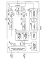
- FIG.4 is a block diagram showing a configuration for an amplifier circuit of a first embodiment of the present invention.
- Amplifier circuit 100 shown in FIG.4 comprises constant-envelope signal generating section 101, pilot signal generating section 102, first addition section 103, second addition section 104, vector adjustment section 105, two D/Aconverters 106a and 106b, two low-pass filters (LPF) 107a and 107b, two mixers 108a and 108b, local oscillator 109, two band pass filters (BPF) 110a and 110b, first amplifier 111, second amplifier 112, combiner 113, pilot signal detector 114, and control section 115.
- LPF low-pass filters
- BPF band pass filters
- pilot signal detector 114 comprises frequency converter 116, LPF 117, and A/D converter 118.
- vector adjustment section 105 comprises amplitude adjustment section 119 and phase adjustment section 120.
- Constant-envelope signal generating section 101 generates two constant-envelope signals, i.e. a first constant-envelope signal S ⁇ a 1 and second constant-envelope signal S ⁇ a 2 using baseband input signals Si and Sq.
- the constant-envelope signals is generated to be equivalent to signals obtained by orthogonally modulating the input signals Si, Sq using a carrier frequency of frequency ⁇ a at the time of vector combining, and outputs these signals to the first addition section 103 and second addition section 104, respectively.
- the pilot signal generating section 102 generates two pilot signals of a frequency outside the band of the input signals Si and Sq, i.e. a first pilot signal and a second pilot signal, and outputs these signals to the first addition section 103 and second addition section 104.
- First addition section 103 adds the respectively inputted first constant-envelope signal S ⁇ a 1 and first pilot signal.
- Second addition section 104 adds the respectively inputted second constant-envelope signal S ⁇ a 2 and second pilot signal.
- Vector adjustment section 105 is, for example, a calculation circuit, and changes the gain and phase of the output signal of the second addition section 104 based on control of control section 115 described later, for output to D/A converter 106b.
- amplitude adjustment section 119 adjusts the gain (amplitude direction) of an output signal of second addition section 104 based on control of control section 115
- phase adjustment section 120 adjusts the phase (phase direction) of the output signal of second addition section 104 based on control of control section 115.
- constant-envelope signal generating section 101, pilot signal generating section 102, first addition section 103, second addition section 104 and vector adjustment section 105 are digital signal processing circuits configured from, for example, a DSP (Digital Signal Processor), CPU (Central Processing Unit), or ASIC (Application Specific Integrated Circuit) or the like, and their respective operations are processed by means of digital signal calculation.
- DSP Digital Signal Processor
- CPU Central Processing Unit
- ASIC Application Specific Integrated Circuit
- D/A converter 106a subjects the first constant-envelope signal S ⁇ a 1 to which the first pilot signal has been added by the first addition section 103 to digital to analog conversion.
- D/A converter 106b converts an output signal from vector adjustment section 105 that is the second constant-envelope signal S ⁇ a 2 with the secondpilot signal added from a digital to analog signal.
- LPF 107a and 107b remove the sampling frequency and folding noise components from each output signal from D/A converters 106a and 106b, and outputs the first constant-envelope signal S ⁇ a 1 and second constant-envelope signal S ⁇ a 2 after the removal to mixers 108a and 108b.
- Mixers 108a and 108b are, for example, mixer circuits for up-converting frequencies, and mix each output signal from LPF 107a and 107b with a local oscillation signal from local oscillator 109 and frequency-converts (up-converts) the first constant-envelope signal S ⁇ a 1 and second constant-envelope signal S ⁇ a 2 after the mixing to a predetermined frequency for output signals, respectively.
- Local oscillator 109 is an oscillation circuit such as a frequency combiner or the like employing a voltage controlledoscillator (VCO) controlled by a phase-locked loop (PLL), and outputs the local oscillation signal to mixers 108a and 108b.
- VCO voltage controlledoscillator
- PLL phase-locked loop
- BPF 110a and 110b are filters for passing signals of a desired frequency band and suppressing unnecessary frequency components.
- the unnecessary frequency components contained in the first constant-envelope signal S ⁇ c 1 and second constant-envelope signal S ⁇ c 2 up-converted by mixers 108a and 108b, i.e. image components generated by mixers 108a and 108b and leakage components of the local oscillation signal are suppressed, and the first constant-envelope signal S ⁇ c 1 and second constant-envelope signal S ⁇ c 2 after the suppression are outputted to first amplifier 111 and second amplifier 112, respectively.
- First amplifier 111 amplifies the output signal from BPF 110a and outputs this to combiner 113.
- Second amplifier 112 amplifies the output signal from BPF 110b and outputs this to combiner 113.
- Pilot signal detector 114 extracts a pilot signal component from a part of the output signal from combiner 113 and outputs this to control section 115. A component corresponding to the first pilot signal and a component corresponding to the second pilot signal are contained in the pilot signal component.
- frequency converter 116 frequency-converts the pilot signal component contained in the signal obtained from combiner 113 to a low frequency band, and outputs this to LPF 117 .
- LPF 117 suppresses an output signal component from the signal frequency-converted at frequency converter 116, and outputs the pilot signal component to A/D converter 118.
- A/D converter 118 converts the pilot signal component from LPF 117 from analog to digital for output to control section 115.
- Control section 115 is configured from a calculation circuit such as a CPU, DSP, ASIC and the like and a memory and the like, and controls adjustment of the gain and phase of vector adjustment section 105 based on the pilot signal components (i.e. the firstpilot signal component and second pilot signal component) outputted by pilot signal detector 114.
- a calculation circuit such as a CPU, DSP, ASIC and the like and a memory and the like, and controls adjustment of the gain and phase of vector adjustment section 105 based on the pilot signal components (i.e. the firstpilot signal component and second pilot signal component) outputted by pilot signal detector 114.
- control section 115 sets the adjustment amount ⁇ in an amplitude direction to a value in such a manner that amplitude components of the first pilot signal component and second pilot signal component detected by pilot signal detector 114 are equal to each other, and sets the adjustment amount ⁇ in the phase direction to a value in such a manner that phase components of the first pilot signal component and secondpilot signal component detected by pilot signal detector 114 are equal to each other.
- the first constant-envelope signal S ⁇ a 1 (t) and second constant-envelope signal S ⁇ a 2 (t) are generated from the baseband input signals Si and Sq.
- the output signals S' ⁇ a 1 (t), and S' ⁇ a 2 (t) at first addition section 103 and second addition section 104 are expressed with (equation 7) and (equation 8), respectively.
- the output signal S' ⁇ a 1 (t) of first addition section 103 is converted to an analog signal
- the output signal Soutv (t) of vector adjustment section 105 is converted to an analog signal at D/A converter 106b.
- the carrier frequency of the signal after the suppression of the noise components are then respectively converted to ⁇ c at mixers 108a and 108b.
- An output signal from BPF 110a is amplified by first amplifier 111, and an output signal from BPF 110b is amplified by second amplifier 112.
- first amplifier 111 and second amplifier 112 a signal that is a constant-envelope signal having a converted frequency ⁇ c and added with a pilot signal is amplified.
- the signals amplified by first amplifier 111 and second amplifier 112 are therefore not a perfect constant-envelope signal but when the amplitudes of the pilot signals are made sufficiently small compared to the constant-envelope signals, envelope fluctuations of the signals amplified here can be made extremely small. For example, if the pilot signal level is made to be a level 40dB lower than the constant-envelope signals, then envelope fluctuation of the amplified signals will be in the order of 1% of amplitude. It is therefore possible for first amplifier 111 and second amplifier 112 to be used with high power efficiency.
- Output signals from first amplifier 111 and second amplifier 112 are synthesized at combiner 113. An output signal is then obtained of amplifier circuit 100.
- the output signal Souta 1 from first amplifier 111 and the output signal Souta 2 from second amplifier 112 can be expressed as (equation 10) and (equation 11), respectively.
- the output signal S' (t) of combiner 113 is a signal where two signals expressed with (equation 10) and (equation 11) are in-phase added, and can be expressed with the following (equation 12).
- S ′ ( t ) G a ⁇ [ V max / 2 ⁇ cos ⁇ ⁇ c t + ⁇ ( t ) + H a ⁇ ] + G b ⁇ ⁇ ⁇ [ V max / 2 ⁇ cos ⁇ ⁇ c t + ⁇ ( t ) + ⁇ + H b ⁇ ] + G a ⁇ P ⁇ cos ⁇ ( ⁇ c ⁇ ⁇ p 1 ) t + H a ⁇ + G b ⁇ ⁇ ⁇ P ⁇ cos ⁇ ( ⁇ c ⁇ ⁇ p 2 ) t + ⁇ + H b ⁇
- the first term on the right side of (equation 13) described above constitutes a signal component that is the input signal subjected to the orthogonal modulation with a carrier of the angular frequency ⁇ c to give a signal of the gain Ga and the phase shift amount Ha, i.e. a desired signal component amplified with the gain Ga.
- the output signal is converted to a low frequency band.
- the local oscillation frequency to be ⁇ c-2 ⁇ p 2 + ⁇ p 1
- the angular frequency of the third term on the right side of (equation 12) is 2 ⁇ ( ⁇ p 2 - ⁇ p 1 )
- the angular frequency of the fourth term is ⁇ p 2 - ⁇ p 1
- the angular frequency of the first term and second term is 2 ⁇ ⁇ p 2 - ⁇ p 1 .
- the output signal of LPF 117 (the pilot signal component) becomes Ga ⁇ P ⁇ cos ⁇ ( ⁇ p 2 - ⁇ p 1 ) t+Ha ⁇ + Gb ⁇ ⁇ ⁇ P ⁇ cos ⁇ p 2 - ⁇ p 1 ) t+ ⁇ +Hb ⁇ .
- A/D converter 118 then converts the pilot signal component obtained through the separation to a digital signal for output to control section 115.
- Control section 115 then controls adjustment of the gain ⁇ and phase shift amount ⁇ performed by vector adjustment section 105, in such a manner that the amplitude components Ga ⁇ P and Gb ⁇ P and the phase components Ha and ⁇ +Hb at pilot signal component GaxPxcos ⁇ p 2 - ⁇ p 1 ) t+Ha ⁇ +Gb ⁇ P ⁇ cos ⁇ ( ⁇ p 2 - ⁇ p 1 )t+ ⁇ +Hb) converted, to a digital signal are equal to each other respectively.
- the signal expressed with (equation 13) can be obtained as an output signal of amplifier circuit 100.
- gain differences and phase differences in two systems of LINC system amplifier circuit 100 is calculated by comparison of a pilot signal which is a simple signal such as a sine wave or the like at first control section 115. Adjustment (correction) of the amplitude component and phase component is then carried out by vector adjustment section 105 based on the calculated gain differences and phase differences.
- the combiner 113 is ideal in-phase combining means, but according to this embodiment, it is possible to correct the gain differences and phase differences even in cases where there are those differences at the time of combining at the combiner 113.
- the gain and phase are corrected at vector adjustment section 105 but the same operations and effects can be obtained using a variable gain amplifier and variable phase shifter or the like employing an analog circuit.
- a configuration of controlling a bias of first amplifier 111 and second amplifier 112 is adopted as a variable gain means, it is possible to further improve the power efficiency.
- phase adjustment section 120 is used as a variable phase-shifting means but the same operations and effects as described above can be also obtained using a variable delay means in the event that a cause of the phase differences is mainly based on differences in the amount of delay.
- a combiner 113 for the in-phase combining is used but this by no means limits phase characteristics. For example, it is also possible to obtain the same operations and effects if a constant-envelope signal is generated in consideration of the phase shift amount even in cases where a directional coupler that performs combining after a ninety-degree phase shift is used in place of combiner 113.
- Amplifier circuit 200 shown in FIG.7 has pilot signal generating section 201 in place of pilot signal generating section 102 of amplifier circuit 100 shown in FIG.4.
- a feature of this embodiment is that two pilot signals are generated in such a manner that pilot signal components cancel each other out after combined in the event that any differences in gain and phase are not generated from respective signals being outputted from first addition section 103 and second addition section 104 until the signals are combined by the combiner 113.
- amplifier circuit 200 having the above configuration will be described. In addition, similar operations to those of the first embodiment described above will not be described in detail.
- the output signals S' ⁇ a 1 (t), S' ⁇ a 2 (t) at first addition section 103 and second addition section 104 can be expressed with (equation 14) and (equation 15), respectively.
- P 1 (t) and P 2 (t) have the same amplitude and are different each other in phase by 180 degrees, and as such, cancel each other out upon in-phase combining, and it is understood that S ⁇ a (t) and S' ⁇ a (t) indicate the same vector coordinate.
- the output signal S' ⁇ a 2 (t) of second addition section 104 is adjusted by, for example, a factor of ⁇ in an amplitude direction, and by the phase shift amount ⁇ in a phase direction, respectively, based on control of control section 115.
- the output signal Soutv(t) of vector adjustment section 105 can be expressed using the following (equation 16) .
- S out v ( t ) ⁇ ⁇ [ V max / 2 ⁇ cos ⁇ ⁇ a t + ⁇ ( t ) + ⁇ ⁇ + P ⁇ cos ⁇ ⁇ a ⁇ ⁇ p 1 ⁇ t + ⁇ + ⁇ ]
- the output signal Souta 1 from first amplifier 111 and the output signal Souta 2 from second amplifier 112 can be expressed as (equation 17), and (equation 18), respectively.
- the output signal S' (t) of combiner 113 is a signal where two signals expressed with (equation 17) and (equation 18) are in-phase added, and can be expressed with the following (equation 19).
- S ' ( t ) G a ⁇ [ V max / 2 ⁇ cos ⁇ ⁇ c t + ⁇ ( t ) + H a ⁇ + G b ⁇ ⁇ ⁇ [ V max / 2 ⁇ cos ⁇ ⁇ c t + ⁇ ( t ) + ⁇ + H b ⁇ + G a ⁇ P ⁇ cos ⁇ ( ⁇ c ⁇ ⁇ p 1 ) t + H a ⁇ + G b ⁇ ⁇ ⁇ P ⁇ cos ⁇ ( ⁇ c ⁇ ⁇ p 1 ) t + ⁇ + ⁇ + H b ⁇
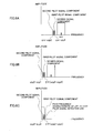
- FIG.9 is a view showing spectrums of output signals for amplifier circuit 200 of this embodiment.
- the third item and fourth item on the right side of (equation 19) are of the same frequency.
- the output signal is converted to a low frequency band.
- the local oscillation frequency to be ⁇ c- ⁇ p 2 -2 ⁇ 10kHz
- the angular frequency of the third term and fourth term on the right side of (equation 19) becomes 2 ⁇ 10kHz
- the angular frequency of the first and second terms becomes ⁇ p 1 +2 ⁇ 10kHz.
- the output signal of LPF 117 (the pilot signal component) becomes Ga ⁇ P ⁇ cos ⁇ (2 ⁇ 10kHz) t+Ha ⁇ +Gb ⁇ y ⁇ P ⁇ cos ⁇ (2 ⁇ 10kHz)t+ ⁇ + ⁇ + Hb ⁇ .
- A/D converter 118 then converts the pilot signal component obtained through the separation to a digital signal for output to control section 115.
- Control section 115 then controls adjustment of the gain ⁇ and phase shift amount ⁇ by vector adjustment section 105 in such a manner that the amplitude components Ga ⁇ P and Gb ⁇ P and the phase components Ha and ⁇ +Hb at the pilot signal component Ga ⁇ P ⁇ cos ⁇ (2 ⁇ 10kHz) t+Ha ⁇ +Gb ⁇ y ⁇ P ⁇ cos ⁇ (2 ⁇ 10kHz) t+ ⁇ + ⁇ + Hb ⁇ converted to a digital signal are equal to each other respectively, i.e., so that the pilot signal components are of the same amplitude but opposite phases and are therefore cancelled out.
- the signal expressed with (equation 20) i.e. the signal with the pilot signal component cancelled, can be obtained as the output signal of amplifier circuit 200.
- gain differences and phase differences in two systems of LINC system amplifier circuit 200 is calculated by comparison of a pilot signal which is a simple signal such as a sine wave or the like using first control section 115. Adjustment (correction) of the amplitude component and phase component is then carried out by vector adjustment section 105 based on the calculated gain differences and phase differences.
- the configuration is such that a pilot signal component converted to a frequency of 10kHz is outputted at control section 115 but this configuration is by no means limiting.
- a detection section is provided at pilot signal detector 114, a detection voltage obtained by the pilot signal component detection is outputted at control section 115, and the control is exerted to adjust the gain ⁇ and the phase shift amount ⁇ by vector adjustment section 105 in such a manner that the detection voltage becomes a minimum, it is possible to make the pilot signal component minimum in the same manner, and the same operations and effects as in the above can be obtained.
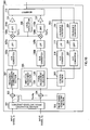
- Amplifier circuit 300 shown in FIG.10 adds frequency characteristic correction section 301 to the configuration of amplifier circuit 100 shown in FIG.4, and adopts a configuration provided with pilot signal detection section 302, control section 303 and pilot signal generating section 304 in place of pilot signal detector 114, control section 115 and pilot signal generating section 102. Further, pilot signal detection section 302 also adopts a configuration where frequency converter 305, LPF 306 and A/D converter 307 are added to the configuration of pilot signal detector 114 described in the first embodiment.
- Pilot signal generating section 304 generates two pilot signals (a first pilot signal and second pilot signal) of a frequency outside the band on the lower side of the input signal, and two pilot signals (a third pilot signal and fourth pilot signal) of a frequency outside the band on the upper side of the input signal. Further, pilot signal generating section 304 outputs the first pilot signal and the third pilot signal to first addition section 103 and outputs the second pilot signal and the fourth pilot signal to second addition section 104.
- First addition section 103 and second addition section 104 add the respectively inputted constant-envelope signals and pilot signals.
- Frequency characteristic compensation section 301 is, for example, a calculation circuit, and changes frequency characteristics of the gain and phase of the output signal of first addition section 103 based on control of control section 303, and then outputs this to D/A converter 106a.
- Frequency characteristic correction section 301 is a digital signal processing circuit comprised of, for example, DSP, CPU, ASIC, or the like, carrying out processing for correction of the frequency characteristics using computation of digital signals. Further, frequency characteristic correction section 301 changes the frequency characteristics for the gain and phase by, for example, changing coefficients of digital filters using digital signal processing.
- Pilot signal detection section 302 extracts a pilot signal component from part of the output signal outputted by combiner 113 and outputs this to control section 303.
- frequency converter 116 frequency-converts into a low frequency band a pilot signal component of a lower frequency outside the band contained in the inputted signal and outputs this to LPF 117.
- LPF 117 suppresses an output signal component from the frequency-converted signal at frequency converter 116 and outputs the pilot signal component of the low frequency outside the band to A/D converter 118.
- A/D converter 118 converts the pilot signal component from LPF 117 from analog to digital for output to control section 303.
- frequency converter 305 frequency-converts to a low frequency band a pilot signal component of a upper frequency outside the band contained in the inputted signal, outputs this to LPF 306.
- LPF 306 suppresses the output signal component from the frequency-converted signal at frequency converter 305 and outputs the pilot signal component of the upper frequency outside the band to A/D converter 307 .
- A/D converter 307 converts the pilot signal component from LPF 306 from analog to digital for output to control section 303.
- Control section 303 controls adjustment of the gain and phase at vector adjustment section 105 and correction of the frequency characteristics at frequency characteristic correction section 301 based on the first to fourth pilot signal components outputted by pilot signal detection section 302.
- control section 303 sets the amount of adjustment ⁇ in an amplitude direction to a value in such a manner that the amplitude components of the first pilot signal component and the second pilot signal component detected by pilot signal detection section 302 are equal to each other, and sets the amount of adjustment ⁇ in a phase direction to a value in such a manner that the phase components of the first pilot signal component and the second pilot signal component detected by pilot signal detector 302 are equal to each other.
- FIG.11 is a view showing an example of gain frequency characteristics of a typical high frequency circuit such as an amplifier or mixer. As shown in FIG. 11, in the event that the gain of the high frequency circuit varies depending on a frequency, variation also exists in the frequency characteristics. Because of this, it is necessary to take into consideration that, even if the gain and phase are corrected using only the pilot signal outside the band on one side, these differences become larger at the frequency band on the upper side of the desired signal and distortion occurs in the output signal.
- FIG.12 is a view showing an example of phase frequency characteristics of two paths (shown by a solid line and a broken line) of different amounts of delay.
- differences occur in the amount of delay between a plurality of paths depending on a difference between the lengths of the transmission paths.
- the difference in phase varies depending on a frequency. Because of this, it is necessary to take into consideration that, even if the phase is corrected using only the pilot signal outside the band on one side, these differences become larger at the frequency band on the upper side of the desired signal and distortion occurs in the output signal.
- the frequency characteristics are corrected using the pilot signals of the frequency components outside the band on the lower side and upper sides of the desired signal.
- the spectrum of the output signal of amplifier circuit 300 at this time is shown in FIG.13.
- the gain and phase of the components of the first pilot signal P 1 (t) and second pilot signal P 2 (t) of the frequency outside the band on the lower side included in the output signal at vector adjustment section 105 are adjusted by control section 303 in such a manner that the components cancel each other out. This operation is similar to the operation described in the second embodiment.
- components for the third pilot signal P 3 (t) and fourth pilot signal P 4 (t) are frequency-converted to a low frequency band.
- the local oscillation frequency to be ⁇ c+ ⁇ pi+2 ⁇ 10kHz
- the angular frequency of the third pilot signal component and fourth pilot signal component is converted to 2 ⁇ 10kHz, i.e. the same frequency as the first pilot signal component and second pilot signal component. Because of this, as a result of LPF 306 and A/D converter 307 carrying out the same operation as LPF 117 and A/D converter 118, the pilot signal components of the frequency outside the band on the upper side can be outputted to control section 303.
- adjustment (correction) of the gain and phase at vector adjustment section 105 is controlled by detecting the pilot signal component of the frequency outside the band on the lower side
- correction of the frequency characteristic at frequency characteristic correction section 301 is controlled by detecting a pilot signal component of the frequency outside the band on the upper side.
- variable delay circuit may also be employed as a means for correcting the frequency characteristics for phase.
- a difference in frequency characteristic of two systems of LINC system amplifier circuit 300 is calculated by comparing the pilot signals which are simple signals such as sine waves using control section 303. Correction of frequency characteristics is then carried out by frequency characteristic correction section 301 based on the calculated difference in frequency characteristics. It is therefore possible to obtain an output signal with a higher power efficiency and little distortion.
- FIG.15 is a block diagram showing a configuration for a wireless transceiver apparatus of a fourth embodiment of the present invention.
- Wireless transceiver apparatus 400 shown in FIG.15 is comprised of amplifier circuit 100 described in the first embodiment, antenna 401 for transmitting and receiving wireless signals, an antenna duplexer 402 for duplexing transmission and reception for antenna 401, outputting output signals of amplifier circuit 100 to antenna 401, and outputting signals received by antenna 401 to wireless receiver 403, wireless receiver 403 constituting a circuit for extracting desired received signals from the output signals of antenna duplexer 402, and configured, for example, from a lownoise amplifier, a mixer performing frequency conversion, a filter, a variable gain amplifier, a A/D converter and the like, and modem 404 for modulating signals for audio, images, data and the like to signals to be wirelessly transmitted, and for demodulating signals for audio, images, data and the like from wirelessly received signals.
- modem 404 for modulating signals for audio, images, data and the like to signals to be wireless
- Wireless transceiver apparatus 400 may also adopt a configuration having one of amplifier circuit 200 and amplifier circuit 300 described in the second embodiment and third embodiment, respectively, in place of amplifier circuit 100.
- wireless transceiver apparatus 400 of this embodiment using an amplifier circuit described in either of the above embodiments to amplify signals for transmission, it is possible to make circuit scale small and make a distortion component included in a transmission signal small at low manufacturing costs.
- wireless transceiver apparatus 400 may adopt a configuration where not only is a local oscillation signal outputted by local oscillator 109 provided at amplifier circuit 100 shared by the mixer of wireless receiver 403, but also control section 115 provided at amplifier circuit 100 is used for controls (for example, automatic gain control or the like) at wireless receiver 403. Because of this, it is possible to make the apparatus scale for wireless transceiver apparatus 400 drastically smaller.
- wireless transceiver apparatus 400 it is possible to achieve the same operations and effects as the operations and effects described in any of the first to third embodiments at wireless transceiver apparatus 400, it is possible to make the apparatus scale for wireless transceiver apparatus 400 drastically smaller, it is possible to keep a distortion component included in a transmitted signal to a level that does not hinder communication, and it is possible to receive data without errors at a receiver.
- the wireless transceiver apparatus 400 described in the above embodiments may be applied to a wireless base station apparatus or communication terminal apparatus used in a wireless communication and broadcast network.
- the amplifier circuit and amplifying method of the present invention is effective in obtaining an output signal with high power efficiency and little distortion while suppressing increases in circuit scale of the amplifier circuit, and is useful, for example, as an amplifier circuit for amplifying transmission signals in a transmission apparatus used in wireless communication and broadcast, and as an amplifying method thereof.
Landscapes
- Engineering & Computer Science (AREA)
- Power Engineering (AREA)
- Amplifiers (AREA)
Applications Claiming Priority (2)
| Application Number | Priority Date | Filing Date | Title |
|---|---|---|---|
| JP2003333490A JP3910167B2 (ja) | 2003-09-25 | 2003-09-25 | 増幅回路 |
| PCT/JP2004/013683 WO2005031993A1 (ja) | 2003-09-25 | 2004-09-17 | 増幅回路および増幅方法 |
Publications (3)
| Publication Number | Publication Date |
|---|---|
| EP1667331A1 true EP1667331A1 (de) | 2006-06-07 |
| EP1667331A4 EP1667331A4 (de) | 2008-05-14 |
| EP1667331B1 EP1667331B1 (de) | 2011-06-29 |
Family
ID=34385988
Family Applications (1)
| Application Number | Title | Priority Date | Filing Date |
|---|---|---|---|
| EP04773302A Expired - Lifetime EP1667331B1 (de) | 2003-09-25 | 2004-09-17 | Verstärker-schaltung und verstärkungs-verfahren |
Country Status (5)
| Country | Link |
|---|---|
| US (1) | US7684513B2 (de) |
| EP (1) | EP1667331B1 (de) |
| JP (1) | JP3910167B2 (de) |
| CN (1) | CN100481741C (de) |
| WO (1) | WO2005031993A1 (de) |
Cited By (1)
| Publication number | Priority date | Publication date | Assignee | Title |
|---|---|---|---|---|
| WO2014202112A1 (en) * | 2013-06-17 | 2014-12-24 | Nokia Solutions And Networks Oy | A radio transmitter with amplifier paths having out-phased radio frequency signals |
Families Citing this family (27)
| Publication number | Priority date | Publication date | Assignee | Title |
|---|---|---|---|---|
| US7023933B2 (en) * | 2000-10-20 | 2006-04-04 | Matsushita Electric Industrial Co., Ltd. | Radio communication apparatus |
| US7355470B2 (en) | 2006-04-24 | 2008-04-08 | Parkervision, Inc. | Systems and methods of RF power transmission, modulation, and amplification, including embodiments for amplifier class transitioning |
| US7327803B2 (en) | 2004-10-22 | 2008-02-05 | Parkervision, Inc. | Systems and methods for vector power amplification |
| US8013675B2 (en) | 2007-06-19 | 2011-09-06 | Parkervision, Inc. | Combiner-less multiple input single output (MISO) amplification with blended control |
| US7911272B2 (en) | 2007-06-19 | 2011-03-22 | Parkervision, Inc. | Systems and methods of RF power transmission, modulation, and amplification, including blended control embodiments |
| US20130078934A1 (en) | 2011-04-08 | 2013-03-28 | Gregory Rawlins | Systems and Methods of RF Power Transmission, Modulation, and Amplification |
| ES2492680T3 (es) * | 2006-04-24 | 2014-09-10 | Parkervision, Inc. | Sistemas y procedimientos de transmisión, modulación y amplificación de potencia de RF |
| US8031804B2 (en) | 2006-04-24 | 2011-10-04 | Parkervision, Inc. | Systems and methods of RF tower transmission, modulation, and amplification, including embodiments for compensating for waveform distortion |
| US8315336B2 (en) | 2007-05-18 | 2012-11-20 | Parkervision, Inc. | Systems and methods of RF power transmission, modulation, and amplification, including a switching stage embodiment |
| WO2009005768A1 (en) | 2007-06-28 | 2009-01-08 | Parkervision, Inc. | Systems and methods of rf power transmission, modulation, and amplification |
| JP4945388B2 (ja) * | 2007-09-13 | 2012-06-06 | 株式会社日立製作所 | 無線基地局 |
| WO2009041097A1 (ja) * | 2007-09-27 | 2009-04-02 | Kyocera Corporation | 電力増幅回路ならびにそれを用いた送信機および無線通信機 |
| WO2009145887A1 (en) | 2008-05-27 | 2009-12-03 | Parkervision, Inc. | Systems and methods of rf power transmission, modulation, and amplification |
| CN101621337B (zh) * | 2008-06-30 | 2013-08-07 | 华为技术有限公司 | 一种时延调节装置与方法 |
| CN101729079B (zh) * | 2008-10-13 | 2012-11-07 | 电子科技大学 | 一种linc发射机 |
| EP2509228B1 (de) * | 2010-04-15 | 2013-06-05 | Research In Motion Limited | Kommunikationsvorrichtung mit separater I- und Q-Phasenstromverstärkung mit selektiver Phase und Grösseneinstellung und zugehörige Verfahren |
| KR20140034895A (ko) | 2011-06-02 | 2014-03-20 | 파커비전, 인크. | 안테나 제어 |
| JP5412472B2 (ja) * | 2011-07-06 | 2014-02-12 | アンリツ株式会社 | 信号発生装置及び信号発生方法 |
| CN102420631B (zh) * | 2011-11-04 | 2016-03-30 | 中兴通讯股份有限公司 | 功率放大装置、多模射频收发装置和多模终端 |
| US20150049793A1 (en) * | 2013-08-16 | 2015-02-19 | Qualcomm Incorporated | Interface sharing between digital and radio frequency circuits |
| EP3047348B1 (de) | 2013-09-17 | 2025-03-19 | Parkervision, Inc. | Verfahren für die darstellung einer datenträgerzeitfunktion |
| CN105264768B (zh) * | 2014-01-02 | 2018-10-19 | 华为技术有限公司 | 包络放大器及基站 |
| JP2016119609A (ja) | 2014-12-22 | 2016-06-30 | 富士通株式会社 | 増幅装置 |
| US9754638B1 (en) * | 2015-08-04 | 2017-09-05 | Marvell International Ltd. | Sense amplifier |
| KR20190018152A (ko) * | 2016-06-10 | 2019-02-21 | 에이티 앤드 티 인텔렉추얼 프라퍼티 아이, 엘.피. | 대역 내 기준 신호를 갖는 무선 분산형 안테나 시스템과의 사용을 위한 방법 및 장치 |
| KR20190016555A (ko) * | 2016-06-10 | 2019-02-18 | 에이티 앤드 티 인텔렉추얼 프라퍼티 아이, 엘.피. | 무선 분산형 안테나 시스템과의 사용을 위한 방법 및 장치 |
| JP6769544B2 (ja) * | 2017-03-21 | 2020-10-14 | 日本電気株式会社 | 増幅装置、及び増幅方法 |
Family Cites Families (26)
| Publication number | Priority date | Publication date | Assignee | Title |
|---|---|---|---|---|
| US4401853A (en) * | 1982-08-23 | 1983-08-30 | Fisher Charles B | AM Quadrature stereo systems |
| US5287069A (en) | 1990-02-07 | 1994-02-15 | Fujitsu Limited | Constant-amplitude wave combination type amplifier |
| JP2758682B2 (ja) | 1990-02-07 | 1998-05-28 | 富士通株式会社 | 定振幅波合成形増幅器 |
| JPH0537263A (ja) | 1991-07-30 | 1993-02-12 | Fujitsu Ltd | 定振幅波合成形増幅器 |
| JP3360464B2 (ja) * | 1995-02-13 | 2002-12-24 | 松下電器産業株式会社 | フィードフォワード増幅器 |
| KR100259849B1 (ko) * | 1997-12-26 | 2000-06-15 | 윤종용 | 파일럿 톤 호핑을 이용한 피드 포워드 선형 전력 증폭 방법 |
| US6054894A (en) | 1998-06-19 | 2000-04-25 | Datum Telegraphic Inc. | Digital control of a linc linear power amplifier |
| JP3570898B2 (ja) | 1998-08-24 | 2004-09-29 | 日本電気株式会社 | プレディストーション回路 |
| US6411644B1 (en) * | 1998-09-29 | 2002-06-25 | Lucent Technologies Inc. | Frequency hop pilot technique for a control system that reduces distortion produced by electrical circuits |
| KR100362925B1 (ko) * | 1999-03-31 | 2002-11-29 | 가부시키가이샤 엔.티.티.도코모 | 피드포워드 증폭기 |
| JP3989731B2 (ja) * | 1999-09-17 | 2007-10-10 | 株式会社エヌ・ティ・ティ・ドコモ | フィードフォワード多端子電力合成形電力増幅器 |
| JP2001148661A (ja) | 1999-11-18 | 2001-05-29 | Hitachi Kokusai Electric Inc | 光伝送システムとその歪み補償方法 |
| JP3877937B2 (ja) * | 2000-05-18 | 2007-02-07 | 株式会社エヌ・ティ・ティ・ドコモ | フィードフォワード増幅器 |
| JP2001339251A (ja) * | 2000-05-25 | 2001-12-07 | Mitsubishi Electric Corp | フィードフォワード増幅器 |
| US6674324B1 (en) | 2000-08-24 | 2004-01-06 | Lucent Technologies Inc. | System and method for producing an amplified signal using plurality of amplitudes across spectrum |
| US6452446B1 (en) * | 2000-12-29 | 2002-09-17 | Spectrian Corporation | Closed loop active cancellation technique (ACT)-based RF power amplifier linearization architecture |
| US6750706B2 (en) * | 2001-06-11 | 2004-06-15 | Matsushita Electric Industrial Co., Ltd. | Control method and circuit for feedforward distortion compensation amplifier |
| JP3911444B2 (ja) | 2001-06-11 | 2007-05-09 | 松下電器産業株式会社 | フィードフォワード歪補償増幅器の制御回路およびフィードフォワード歪補償増幅器 |
| US6496062B1 (en) * | 2001-07-13 | 2002-12-17 | Lucent Technologies Inc. | Predistortion system and method using a pilot signal |
| CN1215727C (zh) | 2001-11-06 | 2005-08-17 | 株式会社Ntt都科摩 | 具有双重环路的前馈放大器 |
| JP2003209445A (ja) | 2001-11-06 | 2003-07-25 | Ntt Docomo Inc | 二重ループを持つフィードフォワード増幅器 |
| JP2003273658A (ja) * | 2002-03-15 | 2003-09-26 | Hitachi Kokusai Electric Inc | フィードフォワード増幅回路 |
| JP2004064377A (ja) * | 2002-07-29 | 2004-02-26 | Hitachi Kokusai Electric Inc | フィードフォワード増幅器 |
| JP2005151543A (ja) * | 2003-10-20 | 2005-06-09 | Matsushita Electric Ind Co Ltd | 増幅回路 |
| US7355470B2 (en) * | 2006-04-24 | 2008-04-08 | Parkervision, Inc. | Systems and methods of RF power transmission, modulation, and amplification, including embodiments for amplifier class transitioning |
| JPWO2006051776A1 (ja) * | 2004-11-11 | 2008-05-29 | 松下電器産業株式会社 | 増幅回路、無線通信回路、無線基地局装置、および無線端末装置 |
-
2003
- 2003-09-25 JP JP2003333490A patent/JP3910167B2/ja not_active Expired - Fee Related
-
2004
- 2004-09-17 CN CNB2004800269811A patent/CN100481741C/zh not_active Expired - Fee Related
- 2004-09-17 US US10/572,577 patent/US7684513B2/en not_active Expired - Fee Related
- 2004-09-17 EP EP04773302A patent/EP1667331B1/de not_active Expired - Lifetime
- 2004-09-17 WO PCT/JP2004/013683 patent/WO2005031993A1/ja not_active Ceased
Cited By (1)
| Publication number | Priority date | Publication date | Assignee | Title |
|---|---|---|---|---|
| WO2014202112A1 (en) * | 2013-06-17 | 2014-12-24 | Nokia Solutions And Networks Oy | A radio transmitter with amplifier paths having out-phased radio frequency signals |
Also Published As
| Publication number | Publication date |
|---|---|
| JP2005101940A (ja) | 2005-04-14 |
| CN100481741C (zh) | 2009-04-22 |
| CN1853351A (zh) | 2006-10-25 |
| US7684513B2 (en) | 2010-03-23 |
| JP3910167B2 (ja) | 2007-04-25 |
| EP1667331A4 (de) | 2008-05-14 |
| US20070076814A1 (en) | 2007-04-05 |
| EP1667331B1 (de) | 2011-06-29 |
| WO2005031993A1 (ja) | 2005-04-07 |
Similar Documents
| Publication | Publication Date | Title |
|---|---|---|
| EP1667331B1 (de) | Verstärker-schaltung und verstärkungs-verfahren | |
| US20070030063A1 (en) | Amplifier circuit | |
| JP3570898B2 (ja) | プレディストーション回路 | |
| US7072421B2 (en) | IQ modulation systems and methods that use separate phase and amplitude signal paths and perform modulation within a phase locked loop | |
| US20080039024A1 (en) | Amplifying Circuit, Radio Communication Circuit, Radio Base Station Device and Radio Terminal Device | |
| US8867596B2 (en) | Methods and apparatuses of calibrating I/Q mismatch in communication circuit | |
| JP2000286915A (ja) | 信号変調回路及び信号変調方法 | |
| US7358829B2 (en) | Transmission apparatus, communication apparatus and mobile radio apparatus | |
| US7496333B2 (en) | Transmission circuit and communication apparatus employing the same | |
| US7769358B2 (en) | Radio system, radio transmitter, and radio receiver | |
| US7613251B2 (en) | Distortion compensating apparatus and method | |
| JP2011146979A (ja) | 送信装置、無線通信装置及び送信方法 | |
| JP2008072735A (ja) | Iq変調システム並びに個別的な位相パス及び信号パスを使用する方法 | |
| US20050078768A1 (en) | Adaptive phase controller, method of controlling a phase and transmitter employing the same | |
| JP2004356835A (ja) | 送信装置および受信装置 | |
| US20060068725A1 (en) | Feedback control loop for amplitude modulation in a polar transmitter with a translational loop | |
| JP2010213107A (ja) | 通信装置 | |
| JP2006203673A (ja) | 送信増幅回路 | |
| JP2006129402A (ja) | 増幅回路及び送信機 | |
| US10587436B2 (en) | Signal transmitter device, detection circuit, and signal detection method thereof | |
| JP2006157256A (ja) | 送信回路、無線通信回路、無線基地局装置、及び無線端末装置 | |
| EP1724956A1 (de) | Funksystem und funkkommunikationsvorrichtung | |
| JP2006253749A (ja) | 歪み補償装置及びその方法 | |
| US6215986B1 (en) | Reducing radio transmitter distortion | |
| US20050143025A1 (en) | Transmitting apparatus |
Legal Events
| Date | Code | Title | Description |
|---|---|---|---|
| PUAI | Public reference made under article 153(3) epc to a published international application that has entered the european phase |
Free format text: ORIGINAL CODE: 0009012 |
|
| 17P | Request for examination filed |
Effective date: 20060323 |
|
| AK | Designated contracting states |
Kind code of ref document: A1 Designated state(s): DE FR GB |
|
| DAX | Request for extension of the european patent (deleted) | ||
| RBV | Designated contracting states (corrected) |
Designated state(s): DE FR GB |
|
| A4 | Supplementary search report drawn up and despatched |
Effective date: 20080414 |
|
| 17Q | First examination report despatched |
Effective date: 20080430 |
|
| RAP1 | Party data changed (applicant data changed or rights of an application transferred) |
Owner name: PANASONIC CORPORATION |
|
| GRAP | Despatch of communication of intention to grant a patent |
Free format text: ORIGINAL CODE: EPIDOSNIGR1 |
|
| GRAS | Grant fee paid |
Free format text: ORIGINAL CODE: EPIDOSNIGR3 |
|
| GRAA | (expected) grant |
Free format text: ORIGINAL CODE: 0009210 |
|
| AK | Designated contracting states |
Kind code of ref document: B1 Designated state(s): DE FR GB |
|
| REG | Reference to a national code |
Ref country code: GB Ref legal event code: FG4D |
|
| REG | Reference to a national code |
Ref country code: DE Ref legal event code: R096 Ref document number: 602004033299 Country of ref document: DE Effective date: 20110825 |
|
| PLBE | No opposition filed within time limit |
Free format text: ORIGINAL CODE: 0009261 |
|
| STAA | Information on the status of an ep patent application or granted ep patent |
Free format text: STATUS: NO OPPOSITION FILED WITHIN TIME LIMIT |
|
| 26N | No opposition filed |
Effective date: 20120330 |
|
| REG | Reference to a national code |
Ref country code: DE Ref legal event code: R097 Ref document number: 602004033299 Country of ref document: DE Effective date: 20120330 |
|
| PGFP | Annual fee paid to national office [announced via postgrant information from national office to epo] |
Ref country code: GB Payment date: 20120912 Year of fee payment: 9 |
|
| PGFP | Annual fee paid to national office [announced via postgrant information from national office to epo] |
Ref country code: DE Payment date: 20120912 Year of fee payment: 9 Ref country code: FR Payment date: 20120926 Year of fee payment: 9 |
|
| GBPC | Gb: european patent ceased through non-payment of renewal fee |
Effective date: 20130917 |
|
| REG | Reference to a national code |
Ref country code: DE Ref legal event code: R119 Ref document number: 602004033299 Country of ref document: DE Effective date: 20140401 |
|
| REG | Reference to a national code |
Ref country code: FR Ref legal event code: ST Effective date: 20140530 |
|
| PG25 | Lapsed in a contracting state [announced via postgrant information from national office to epo] |
Ref country code: GB Free format text: LAPSE BECAUSE OF NON-PAYMENT OF DUE FEES Effective date: 20130917 |
|
| PG25 | Lapsed in a contracting state [announced via postgrant information from national office to epo] |
Ref country code: FR Free format text: LAPSE BECAUSE OF NON-PAYMENT OF DUE FEES Effective date: 20130930 Ref country code: DE Free format text: LAPSE BECAUSE OF NON-PAYMENT OF DUE FEES Effective date: 20140401 |