EP1668832B1 - Skalierbare verbindungen von einrichtung zu einrichtung - Google Patents
Skalierbare verbindungen von einrichtung zu einrichtung Download PDFInfo
- Publication number
- EP1668832B1 EP1668832B1 EP04781551A EP04781551A EP1668832B1 EP 1668832 B1 EP1668832 B1 EP 1668832B1 EP 04781551 A EP04781551 A EP 04781551A EP 04781551 A EP04781551 A EP 04781551A EP 1668832 B1 EP1668832 B1 EP 1668832B1
- Authority
- EP
- European Patent Office
- Prior art keywords
- data
- signal
- lane
- mii
- transmitting
- Prior art date
- Legal status (The legal status is an assumption and is not a legal conclusion. Google has not performed a legal analysis and makes no representation as to the accuracy of the status listed.)
- Expired - Lifetime
Links
- 230000005540 biological transmission Effects 0.000 claims description 21
- 238000004891 communication Methods 0.000 claims description 16
- 238000000034 method Methods 0.000 claims description 11
- 239000004744 fabric Substances 0.000 claims description 2
- 239000000835 fiber Substances 0.000 claims description 2
- 230000004044 response Effects 0.000 description 9
- 238000010586 diagram Methods 0.000 description 7
- 239000004065 semiconductor Substances 0.000 description 3
- 229910000679 solder Inorganic materials 0.000 description 3
- RYGMFSIKBFXOCR-UHFFFAOYSA-N Copper Chemical compound [Cu] RYGMFSIKBFXOCR-UHFFFAOYSA-N 0.000 description 2
- 229910052802 copper Inorganic materials 0.000 description 2
- 239000010949 copper Substances 0.000 description 2
- 230000008878 coupling Effects 0.000 description 2
- 238000010168 coupling process Methods 0.000 description 2
- 238000005859 coupling reaction Methods 0.000 description 2
- 230000003247 decreasing effect Effects 0.000 description 2
- 230000014509 gene expression Effects 0.000 description 2
- 238000012986 modification Methods 0.000 description 2
- 230000004048 modification Effects 0.000 description 2
- 238000012545 processing Methods 0.000 description 2
- 238000011084 recovery Methods 0.000 description 2
- 230000000630 rising effect Effects 0.000 description 2
- 230000011664 signaling Effects 0.000 description 2
- 239000004606 Fillers/Extenders Substances 0.000 description 1
- 230000001419 dependent effect Effects 0.000 description 1
- 238000013461 design Methods 0.000 description 1
- 238000001514 detection method Methods 0.000 description 1
- 238000003780 insertion Methods 0.000 description 1
- 230000037431 insertion Effects 0.000 description 1
- 230000003287 optical effect Effects 0.000 description 1
- 238000005457 optimization Methods 0.000 description 1
- 238000005192 partition Methods 0.000 description 1
- 230000001360 synchronised effect Effects 0.000 description 1
- 230000002123 temporal effect Effects 0.000 description 1
Images

Classifications
-
- H—ELECTRICITY
- H04—ELECTRIC COMMUNICATION TECHNIQUE
- H04L—TRANSMISSION OF DIGITAL INFORMATION, e.g. TELEGRAPHIC COMMUNICATION
- H04L12/00—Data switching networks
- H04L12/28—Data switching networks characterised by path configuration, e.g. LAN [Local Area Networks] or WAN [Wide Area Networks]
- H04L12/40—Bus networks
-
- H—ELECTRICITY
- H04—ELECTRIC COMMUNICATION TECHNIQUE
- H04L—TRANSMISSION OF DIGITAL INFORMATION, e.g. TELEGRAPHIC COMMUNICATION
- H04L12/00—Data switching networks
- H04L12/28—Data switching networks characterised by path configuration, e.g. LAN [Local Area Networks] or WAN [Wide Area Networks]
- H04L12/40—Bus networks
- H04L12/4013—Management of data rate on the bus
- H04L12/40136—Nodes adapting their rate to the physical link properties
-
- H—ELECTRICITY
- H04—ELECTRIC COMMUNICATION TECHNIQUE
- H04L—TRANSMISSION OF DIGITAL INFORMATION, e.g. TELEGRAPHIC COMMUNICATION
- H04L7/00—Arrangements for synchronising receiver with transmitter
- H04L7/0008—Synchronisation information channels, e.g. clock distribution lines
Definitions
- the subject matter disclosed herein relates to interfaces between devices.
- the subject matter disclosed herein relates to devices capable of transmitting or receiving data at more than one data rate.
- DDI device-to-device interconnection
- a device may be coupled to a DDI by solder bonding or a device socket secured to the PCB.
- IEEE Std. 802.3ae - 2002 Clause 47 defines a 10 Gigabit Attachment Unit Interface (XAUI) for transmitting data between devices in data lanes. Each data lane typically transmits a serial data signal between the devices using a differential signaling pair.
- a XAUI is typically coupled to a 10 Gigabit Media Independent Interface (XGMII) which is capable of transmitting or receiving data at a data rate of ten gigabits per second.
- XGMII 10 Gigabit Media Independent Interface
- the XAUI format may be used in transmitting data over an Infiniband 4x cable as described in the proposed 10GBASE-CX4 standard presently being explored by the IEEE P802.3ak working group.
- the present invention provides a device as set out in claim 1 and a method as set out in claim 11.
- Machine-readable instructions as referred to herein relate to expressions which may be understood by one or more machines for performing one or more logical operations.
- machine-readable instructions may comprise instructions which are interpretable by a processor compiler for executing one or more operations on one or more data objects.
- this is merely an example of machine-readable instructions and embodiments of the present invention are not limited in this respect.
- Machine-readable medium as referred to herein relates to media capable of maintaining expressions which are perceivable by one or more machines.
- a machine-readable medium may comprise one or more storage devices for storing machine-readable instructions or data.
- Such storage devices may comprise storage media such as, for example, optical, magnetic or semiconductor storage media.
- storage media such as, for example, optical, magnetic or semiconductor storage media.
- logic as referred to herein relates to structure for performing one or more logical operations.
- logic may comprise circuitry which provides one or more output signals based upon one or more input signals.
- Such circuitry may comprise a finite state machine which receives a digital input and provides a digital output, or circuitry which provides one or more analog output signals in response to one or more analog input signals.
- Such circuitry may be provided in an application specific integrated circuit (ASIC) or field programmable gate array (FPGA).
- ASIC application specific integrated circuit
- FPGA field programmable gate array
- logic may comprise machine-readable instructions stored in a memory in combination with processing circuitry to execute such machine-readable instructions.
- these are merely examples of structures which may provide logic and embodiments of the present invention are not limited in this respect.
- a "device-to-device interconnection" as referred to herein relates to a data link to transmit data between devices.
- a DDI may be formed by conductive traces formed on a circuit board between device sockets to receive devices.
- a DDI may traverse multiple devices coupled between two devices over a backplane and comprise conductive traces coupling the devices to one another.
- a DDI may comprise a cable coupled between two connectors at opposite ends of the cable. Each connector may then transmit data between the cable and a device coupled to the connector by conductive traces.
- a data link formed in a DDI may comprise a plurality of "data lanes" where each data lane may transmit data from a source to a destination independently of other data lanes. Each data lane in a data link may transmit symbols in a transmission medium which are decoded into data bits at a destination.
- a "data lane pair" or “pair of data lanes” as referred to herein relates to two data lanes coupled between a first and second device including a first data lane to transmit data from the first device to the second device and a second data lane to transmit data from the second device to the first device.
- a "data lane interface" as referred to herein relates to a portion of a device that is capable of transmitting a signal to or receiving a signal from a data lane.
- a data lane interface may comprise conductive pins that are capable of being coupled to a data lane formed in a printed circuit board by, for example, solder bonding or a device socket.
- a data lane interface may comprise conductive pins that are capable of being coupled to a cable through a cable connector.
- a "serial data signal" as referred to herein relates to a signal comprising information encoded into a series of symbols.
- a serial data signal may comprise a series of symbols transmitted in a transmission medium where each symbol is transmitted in a symbol period.
- this is merely an example of a serial data signal and embodiments of the present invention are not limited in these respects.
- a "differential pair signal” as referred to herein relates to a pair of synchronized signals to transmit encoded data to a destination.
- differential pair may transmit a serial data signal comprising symbols to be decoded for data recovery at a destination.
- Such a differential pair may transmit each symbol as a voltage on each of two transmission media.
- these are merely examples of a differential pair and embodiments of the present invention are not limited in these respects.
- a data lane interface may be actively transmitting a serial data signal when coupled to a data lane and, at least periodically in the presence of data to be transmitted, applying voltage signals to a data lane contact.
- Actively receiving as referred to herein relates to a state of data lane interface in receiving data from a data lane.
- a data lane interface may be actively receiving a serial data signal when coupled to a data lane and, at least periodically when the data lane is transmitting voltages to the data lane interface, receiving one or more voltage signals from the data lane.
- these are merely examples of when a data lane interface may be actively transmitting or actively receiving, and embodiments of the present invention are not limited in these respects.
- An “8B10B encoding scheme” as referred to herein relates to a process by which eight-bit data bytes may be encoded into ten-bit "code groups," or a process by which ten-bit code groups may be decoded to eight-bit data bytes.
- An “8B10B encoder” as referred to herein relates to logic to encode an eight-bit data byte to a ten-bit code group, and an “8B10B decoder” as referred to herein relates to logic to decode an eight-bit byte from a ten-bit code group.
- An “8B10B codec” as referred to herein relates to a combination of an 8B10B encoder and an 8B10B decoder.
- a "state machine” as referred to herein relates to logic that may define one or more states.
- a state machine may respond to inputs by changing one or more of its states.
- a state machine may receive a data input from a source and provide a data output to a destination where the data output is indicative of one or more states of the state machine. Such a data output may be provided to the destination in a particular data format and at a particular data rate.
- these are merely examples of a state machine and embodiments of the present invention are not limited in these respects.
- a "media independent interface” as referred to herein relates to an interface to receive data from a source or transmit data to a destination in a format which is independent of a particular transmission medium for transmitting the data.
- a data transceiver may transmit data to a transmission medium in a data transmission format in response to data received at an MII.
- a data transceiver may provide data to an MII in response to receiving data from a transmission medium in a data transmission format.
- An MII may also receive data from or provide data to a state machine coupled to one or more data lanes in a DDI.
- a "Gigabit MII” (GMII) as referred to herein relates to an MII capable of receiving data from a source or transmitting data to a destination at a data rate of about one gigabit per second.
- a "10 Gigabit MII” (XGMII) as referred to herein relates to an MII capable of receiving data from a source or transmitting data to a destination at a data rate of about ten gigabits per second.
- XGMII 10 Gigabit MII
- these are merely examples of an MII and embodiments of the present invention are not limited in these respects.
- An “attachment unit interface” (AUI) as referred to herein relates to a physical medium capable of transmitting data between an attachment to a transmission medium of data network and data terminal equipment.
- An “Extended Attachment Unit Interface” as referred to herein relates to a data link capable of transmitting data between an NII and data transceiver.
- a “10 Gigabit Extended Attachment Unit Interface” (XAUI) as referred to herein relates to an extended attachment unit interface capable of transmitting data between an XGMII and a data transceiver.
- Other Extended Attachment Unit Interfaces may be defined for higher data rates such as 40 or 100 gigabits per second.
- an embodiment of the present invention relates to a device to transmit data to or receive data from one or more data lane interfaces at a data rate.
- Each data lane interface may be capable of transmitting a serial data signal to or receiving a serial data signal from a data lane in a device-to-device interconnection.
- the data rate may be varied based, at least in part, upon a number of the data lane interfaces actively transmitting a serial data signal to or actively receiving a serial data signal from the device-to-device interconnection.
- this is merely an exemplary embodiment and other embodiments of the present invention are not limited in these respects.
- Figure 1 shows a schematic diagram of devices 12 coupled by a DDI 14 according to an embodiment of the present invention.
- the DDI 14 may comprise a plurality of data lanes (not shown) formed in copper traces of a printed circuit board (not shown) or in a cable coupled between the devices 12.
- Each data lane may transmit or receive data in one or more differential pair signals.
- this is merely an example of how data may be transmitted in a data lane and embodiments of the present invention are not limited in this respect.
- a corresponding pair of data lanes may employ two differential pair signals (e.g., one differential pair signal for transmitting data from a device on a first data lane and one differential signaling pair for receiving data at the device on a second data lane).
- a single data lane may employ a single differential pair signal for communicating in a half-duplex operating mode.
- this is merely an example of how full or half duplex communication may be implemented using differential pair signals, and embodiments of the present invention are not limited in these respects.
- the devices 12 and 16 may be coupled to other devices in any one of several data communication systems or input/output architectures.
- either of the devices 12 or 16 may comprise a media independent interface (MII) for coupling to other devices such as a media access controller (MAC) (not shown).
- MII media independent interface
- MAC media access controller
- Such a MAC may couple the device 12 or 16 to any one of several other I/O devices such as, for example, a multiplexed data bus, multi-port switch fabric or backplane Ethernet switch.
- the MAC may also couple the device 12 or 16 to one or more packet classification devices (e.g., for network protocol processing) such as a network processor or packet classification ASIC.
- packet classification devices e.g., for network protocol processing
- the device 12 or 16 may comprise an MII coupled to a physical layer communication device (not shown) for transmitting or receiving data in a transmission medium such as, for example, coaxial, fiber optic or twisted wire pair cabling.
- a transmission medium such as, for example, coaxial, fiber optic or twisted wire pair cabling.
- the device 12 or device 16 may be integrated with a MAC or physical layer communication device independently of an MII.
- the device 12 or device 16 may comprise a transmitting or receiving state machine integrated with the MAC or physical layer communication device independently of a MAC.
- Figures 2 through 4 illustrate the use of a device 22 that is capable of transmitting or receiving data from a DDI having two, four or eight pairs of data lanes.
- the device 22 may also comprise an MII (not shown) to transmit data between the DDI and another device (e.g., a MAC or physical layer communication device, not shown).
- the device 22 may be integrated with a MAC or physical layer communication device independently of such an MII. In either such embodiment, the device 22 may transmit data between the DDI and other device at a data rate.
- each of the data lanes may be capable of transmitting data at a set data rate such as 2.5 gigabits per second (e.g., about 3.125 gigabits per second including overhead), full-duplex.
- a set data rate such as 2.5 gigabits per second (e.g., about 3.125 gigabits per second including overhead), full-duplex.
- this is merely an example data rate for a data lane and other embodiments may be directed to data lanes transmitting data at different rates.
- the device 22 may vary the data rate at which data is transmitted between the DDI and another device (e.g., a MAC or physical layer communication device, not shown) based upon a number of data lanes being used to actively transmit or receive data in the DDI.
- a DDI 24 comprising four pairs of data lanes 28 coupled to a device 22 (where a first data lane in a pair 28 transmits first serial data signal from the device 22 and a second data lane in the pair 28 transmits a second serial data signal away from the device 22) may couple the device 22 to a 10 Gigabit Media Independent Interface Extender Sublayer (XGXS) device 26 to behave according to IEEE Std. 802.3ae-2002, Clause 47.
- the DDI 24 may provide a 10 Gigabit Attachment Unit Interface (XAUI).
- the device 22 may be configured as an XGXS device to transmit data to or receive data from the DDI 24 at a data rate of about 10 gigabits per second.
- a DDI 34 comprising two pairs of data lanes 38 may couple the device 22 to a device 36 capable of transmitting data between the devices 22 and 36 at a data rate of about five gigabits per second (e.g., as a 5000BASE-X device). Accordingly, the device 22 may be configured to transmit data to or receive data from the DDI 24 at a data rate of about five gigabits per second.
- a DDI 44 comprising a single pair of data lanes 48 may couple the device 22 to a device 46 capable of transmitting data between the devices 22 and 46 at a data rate of about 2.5 gigabits per second (e.g., as a 2500 BASE-X device). Accordingly, the device 22 may be configured to transmit data to or receive data from the DDI 44 at a data rate of about 2.5 gigabits per second.
- any of the devices 26, 36 or 46 may similarly be configured to transmit or receive data on one, two or four pairs of data lanes.
- a DDI of one, two or four pairs of data lanes may be used to transmit data between the device 22 and any of the devices 26, 36 or 46.
- Any of these devices 26, 36 or 46 may also have the capability of varying a data rate at which data is transmitted to or received from the DDI based upon a number of data lanes in the DDI.
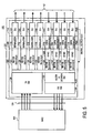
- Figure 5 shows a schematic diagram of a device 102 which is capable of selectively varying a data rate at an MII 124 based upon a number of data lanes 112 actively transmitting or actively receiving data from a DDI according to an embodiment of the device 22 shown in Figures 2 through 4 .
- the device 102 may be formed in one or more semiconductor devices using techniques known to those or ordinary skill in the art of logic design. Alternatively, one or more of the illustrated portions may be implemented machine-readable instructions that are executable by a processor or microcontroller. However, these are merely examples of how a device to transmit data between an MII and a DDI may be implemented and embodiments of the present invention are not limited in these respects.
- the device 102 may comprise a physical medium dependent (PMD) sublayer section 110 capable of transmitting signals to or receiving signals from one or more pairs of data lanes 112, and a physical coding sublayer (PCS) section 106 capable of transmitting data to or receiving data from the MII 124.
- PMD physical medium dependent
- PCS physical coding sublayer
- a physical media attachment (PMA) sublayer section 108 is coupled to the PMD section 110 and PCS section 106 to transmit parallel data signals to the PCS section 106 in response to signals from the PMD section 110, and to transmit encoded data signals to the PMD section 110 in response to parallel data signals from the PCS section 106.
- the PMD section 110 comprises a plurality of data lane interfaces (DLIs) 114 and 115 where each DLI may be coupled to an associated data lane 112.
- Each DLI 114 and 115 may comprise conductive pins (not shown) adapted to being coupled to conductive elements on a printed circuit board by, for example, solder bonding or a device socket.
- each DLI 114 and 115 may be coupled to a cable through a conductive cable connector.
- Each DLI may comprise a set of conductive pins to transmit serial data to, or receive serial data from, an associated data lane 112.
- the associated data lane 112 may transmit serial data signals to or receive serial data signals from the DDI as a differential pair signal.
- the PMA section 108 may comprise a clock and data recovery (CDR) and deserializer circuit 116.
- the CDR portion may generate serial data in response to a differential pair signal from an associated DLI 115.
- the deserializer portion may provide a ten-bit parallel data word to the PCS section 106 on byte intervals.
- a serializer circuit 118 may generate serial data for transmission through the DLI 114 in response to receipt of a ten-bit parallel data word from the PCS section 106 on byte intervals (e.g., through printed circuit board traces or through a connector and cable in a 10GBASE-CX implementation).
- the PCS section 106 may comprise a synchronization circuit 122 and an 8B10B decoder 120.
- the synchronization circuit 122 may detect boundaries between sequential ten bit "code groups" as described in IEEE Std. 802.3ae - 2002, Clause 48.2.4.2.1.
- the 8B10B decoder 120 may then decode the sequential ten bit code groups into eight bit bytes as described in IEEE Std. 802.3 - 2000, Clause 36 and provide the decoded bytes to an alignment and deskew state machine 130.
- an 8B10B encoder 123 may encode each eight bit byte to a ten bit code group for transmission on an associated DLI 114.
- the code groups received at the 8B10B decoder 120 comprise encoded data and control symbols such as an alignment character indicating a temporal alignment of the data received in the data lane.
- the alignment characters may be inserted at random times in the data lanes. For example, the insertion of alignment characters may occur during inter-frame gaps or idle periods to reduce data overhead impacts.
- the 8B10B decoder 120 may indicate the location of detected alignment characters among the decoded eight bit bytes.
- the alignment and deskew state machine 130 may determine the location of alignment characters independently of the 8B10B decoder 120.
- the alignment and deskew state machine 130 may concatenate four aligned bytes forming a 32-bit word to be provided to a receive state machine 128. If a serial data signal is being actively received from four data lanes 112 (as illustrated in Figure 2 ), the alignment and deskew state machine 130 may select an aligned byte from each of the four data lanes to form the 32-bit word. If a serial data signal is being actively received from exactly two data lanes 112 (as illustrated in Figure 3 ), the alignment and deskew state machine 130 may select two aligned bytes received from each of the data lanes 112 to form the 32-bit word. If a serial data signal is being actively received from exactly one data lane 112 (as illustrated in Figure 4 ), the alignment and deskew state machine 130 may combine four consecutive received bytes to form the 32-bit word.
- a "local link fault" received on an inbound or receive path may be detected at a location between the device 102 and a remote device (not shown) coupled to the device 102 by one or more data lanes 112.
- a "remote link fault” provided on an out-bound or transmit path upon detection of a local link fault may be detected at a location beyond the remote device.
- the receive state machine 128 may receive link fault signals indicating such a local or remote link fault from the remote device.
- the transmit state machine 126 may transmit a link fault signal to the remote device indicating a local link fault or a remote link fault (e.g., a link fault detected at a location beyond the MAC 104).
- link fault signals may be received by the receive state machine 128 or transmitted by the transmit state machine 126 as provided in IEEE Std. 802.3ae-2002, Clause 46.3.4.
- four aligned bytes may provide a link fault signal (e.g., a sequence control character in lane 0, data characters 0x00 in lanes 1 and 2, and data character 0x01 in lane 3 to indicate a local link fault or a data character Ox02 to indicate a remote link fault).
- a link fault signal e.g., a sequence control character in lane 0, data characters 0x00 in lanes 1 and 2, and data character 0x01 in lane 3 to indicate a local link fault or a data character Ox02 to indicate a remote link fault.
- a single pair of data lanes is actively transmitting data (i.e., a single DLI 114 is transmitting a serial data signal in a data lane 112 and a single DLI 115 is receiving a serial data signal from a data lane 112)
- four bytes transmitted/received in series may provide the link fault signal (e.g., transmission of a sequence control character, two data characters 0x00, and data character Ox01 to indicate a local link fault or a data character Ox02 to indicate a remote link fault).
- the link fault signal may be transmitted/received in two serial bytes (e.g., a sequence control character followed by a data character Ox01 to indicate a local link fault or a data character Ox02 to indicate a remote link fault).
- link fault signals may be transmitted/received as four bytes, two aligned bytes transmitted in a first byte interval followed by two aligned bytes transmitted in a second byte interval.
- the first two aligned bytes may comprise a sequence control character and a data character 0x00.
- the second two aligned bytes may comprise a data character 0x00 and a data character 0x01 to indicate a local link fault or a data character 0x02 to indicate a remote link fault.
- two aligned bytes may be transmitted in a single byte interval where a first aligned byte provides a sequence control character and the second byte provides a data character 0x01 to indicate a local link fault or a data character 0x02 to indicate a remote link fault.
- the receive state machine 128 may format the 32-bit word for transmission as a 32-bit signal data signal in the MII 124.
- the MII 124 comprises a signal format as provided by an XGMII as described in IEEE Std. 802.3ae - 2002, Clause 46
- the 32-bit word may be formatted for transmission as the signal RXD ⁇ 31:0> along with a control word Roc ⁇ 3:0>.
- the receive state machine 128 may transmit a 32-bit word formatted as RXD ⁇ 31:0> to the MII 124 on intervals of a clock signal RX_CLK such as, for example, on rising and falling edges of the clock signal RX_CLK.
- a transmit state machine 126 may receive a formatted 32-bit word from the MII 124 as, for example, the XGMII signal TXD ⁇ 31:0> along with a control word TXC ⁇ 3:0> on intervals of a clock signal TX_CLK such as, for example, rising and falling edges of the clock signal TX_CLK.
- a clock signal TX_CLK may be generated and controlled by the MAC 104.
- the transmit state machine 126 may partition the 32-bit word among data lanes 112 that are actively transmitting data (e.g., one byte per data lane 112 if four data lanes are actively transmitting, two bytes per data lane 112 if two data lanes are actively transmitting and four bytes on a single data lane 112 if one data lane is actively transmitting).
- the associated 8B10B codec 120 for each actively transmitting data lane 112 may then encode each byte into a corresponding ten bit code group for transmission to the data lane 112 through the PMA section 108 and PMD section 110.
- the device 102 may maintain two clock domains, a first clock domain to control a data rate of the transmit state machine 126 and receive state machine 128 (also, for example, at the MII 124) and a second clock domain to control the transmission and reception of the data at the individual data lanes 112.
- the clock signals TX_CLK or RX_CLK may be referenced to a first common clock signal controlling the first clock domain.
- the first common clock signal may also control the execution of the transmit state machine 126 and the receive state machine 128.
- the data rate at which the transmit state machine 126 transmits data to the data lanes 112 and the data rate at which the receive state machine 128 provides data to the MAC 104 may be increased or decreased.
- the clock signals TX_CLK or RX_CLK may have a frequency of about 156.25 MHz to maintain a data rate at the MII 124 of about ten gigabits per second (e.g., if four data lanes 112 are actively transmitting data and four data lanes 112 are actively receiving data), a frequency of about 78.12 MHz to maintain a data rate at the MII 124 of about five gigabits per second (e.g., if two data lanes 112 are actively transmitting data and two data lanes 112 are actively receiving data), and a frequency of about 39.06 MHz to maintain a data rate at the MII 124 of about 2.5 gigabits per second (e.g., if one data lane 112 is actively transmitting data and one data lane 112 is actively receiving data).
- a second common clock signal may control the CDR and deserializer circuit 116, synchronization circuit 122 and 8B10B decoder 120 that is actively receiving a serial data signal from an associated data lane 112.
- the second common clock signal may control the serializer circuit 118 and 8B10B decoder 123 that is actively transmitting a serial data signal in a corresponding data lane 112.
- the second common clock signal may control the transmission of serial data to or the reception or serial data from a data lane 112 at a fixed data rate (e.g., about 3.215 gigabits per second).
- the slower of the first and second common clock signals may be generated from the faster of the first and second common clock signals using clock dividing circuitry known to those of ordinary skill in the art.
- the first common clock signal of the first clock domain may be controlled based upon an indication of a number of DLIs 115 that are actively transmitting a serial data signal to a data lane 112 or number of DLIs 114 that are actively receiving a serial data signal from a data lane 112.
- the PMD section 110 may provide a four-bit signal signal_detect ⁇ 3:0> to the PCS section 106 indicating which of the DLIs 114 are receiving a signal from an associated data lane 112 (e.g., as provided in IEEE P802.3ak - Clause 54.6.5 where PMD_signal_detect_n indicates whether a data lane n is receiving data).
- the PCS section 106 may receive data in a register of a Management Data Input/Output ("MDIO") Interface as provided in IEEE Std. 802.3ae-2002, Clause 45.
- MDIO Management Data Input/Output
- a PCS section may detect a number of DLIs that may be transmitting data to or receiving data from a data lane, and embodiments of the present invention are not limited in these respects.
- the frequency of the first common clock signal may be set to control the data rate of the MII 124 accordingly.
- a transmit state machine e.g., the transmit state machine 126) and a receive state machine (e.g., the receive state machine 128) may be integrated in a single device with a MAC or physical layer communication device independently of an MII. Accordingly, the transmit state machine may transmit data from the integrated device to a DDI at a data rate based, at least in part, on a number of data lanes actively transmitting a serial data signal. Similarly, the receive state machine may transmit data to the integrated device at a data rate based, at least in part on a number of data lanes actively transmitting a serial data signal.
Landscapes
- Engineering & Computer Science (AREA)
- Computer Networks & Wireless Communication (AREA)
- Signal Processing (AREA)
- Quality & Reliability (AREA)
- Information Transfer Systems (AREA)
- Dc Digital Transmission (AREA)
- Communication Control (AREA)
- Paper (AREA)
- Electrotherapy Devices (AREA)
- Investigating Or Analyzing Materials By The Use Of Ultrasonic Waves (AREA)
Claims (20)
- Vorrichtung, umfassend:eine medienunabhängige Schnittstelle, MII (124) oder eine Zustandsmaschine zum Übertragen und/oder Empfangen von Daten mit einer Übertragungsgeschwindigkeit;eine Vielzahl von Datenspurschnittstellen (114, 115), wobei jede Datenspurschnittstelle bedienbar ist, um ein serielles Datensignal an eine Datenspur zu übertragen oder ein serielles Datensignal von einer Datenspur (28, 38, 48, 112) in einher Verbindung von Vorrichtung zu Vorrichtung zu empfangen, wobei jede Datenspur durch eine zugehörige Datenspurschnittstelle mit der MII oder der Zustandsmaschine gekoppelt ist,
gekennzeichnet durchLogik, um die Übertragungsgeschwindigkeit zu variieren, basierend zumindest teilweise auf einer Reihe von Datenspurschnittstellen, die aktiv ein serielles Datensignal an die Verbindung von Vorrichtung zu Vorrichtung übertragen oder aktiv ein serielles Datensignal von dieser Verbindung empfangen. - Vorrichtung nach Anspruch 1, wobei jede Datenspurschnittstelle (114, 115) mit einem ersten Differentialpaar zum Übertragen eines seriellen Datensignals und einem zweiten Differentialpaar zum Empfangen eines seriellen Datensignals verbunden ist.
- Vorrichtung nach Anspruch 2, wobei die vielzahl von Datenspurschnittstellen (114, 115) bedienbar ist, um Daten an eine 10 Gigabit Anschlusseinheitsschnittstelle zu übertragen und von ihr Daten zu empfangen.
- Vorrichtung nach Anspruch 1, wobei die Vorrichtung ferner umfasst:eine vielzahl von 8B10B-Decodern (120), wobei jeder 8B10B-Dekoder mit einer der Datenspurschnittstellen verbunden und jeder 8B10B-Decoder bedienbar ist, um ein 8Bit-Byte aus einem Differentialpaar an ersten Intervallen eines ersten Taktsignals zu dekodieren;eine Empfangszustandsmaschine (128), um der MII an zweiten Intervallen eines zweiten Taktsignals ein Datensignal fester Länge bereitzustellen; undLogik, um die zweiten Intervalle zu variieren, basierend auf einer Reihe von Datenspurschnittstellen, die aktiv Daten von der Verbindung von Vorrichtung zu Vorrichtung empfangen.
- Vorrichtung nach Anspruch 1, wobei die Vorrichtung ferner umfasst:eine Übertragungszustandsmaschine (126), um ein Datensignal fester Länge von der MII in den ersten Intervallen eines ersten Taktsignals zu empfangen;eine Vielzahl von 8B10B-Encodern (123), wobei jeder 8B10B-Encoder mit einer der Datenspurschnittstellen verbunden und jeder 8B10B-Encoder bedienbar ist, um ein 8Bit-Byte des Datensignals fester Länge zur Übertragung an ein Differentialpaar in zweiten Intervallen eines zweiten Taktsignals zu kodieren;Logik, um die zweiten Intervalle zu variieren, basierend auf einer Reihe von Datenspurschnittstellen, die aktiv Daten von der Verbindung von Vorrichtung zu Vorrichtung übertragen.
- Vorrichtung nach Anspruch 1, wobei die Verbindung von Vorrichtung zu Vorrichtung Leiterplattenbahnen umfasst.
- Vorrichtung nach Anspruch 1, wobei die Verbindung von Vorrichtung zu Vorrichtung ein Kabel umfasst.
- System, umfassend:eine Medienzugangssteuerung MAC (104); undeine mit der MAC gekoppelte Kommunikationsvorrichtung, wie in einem der Ansprüche 1 bis 7 dargestellt.
- System nach Anspruch 8, wobei das System ferner eine mit der MAC gekoppelte Switch-Fabric umfasst.
- System nach Anspruch 8, wobei das System ferner eine mit der MAC gekoppelte Paketklassifikationsvorrichtung umfasst.
- Verfahren, umfassend:mindestens entweder das Übertragen von Daten an oder Empfangen von Daten von einer medienunabhängigen Schnittstelle, MII (124), oder Zustandsmaschine mit einer Übertragungsgeschwindigkeit;Übertragen eines seriellen Datensignals an oder Empfangen eines seriellen Datensignals von einer oder mehreren Datenspuren (28, 38, 48, 112) in einer Verbindung von Vorrichtung zu Vorrichtung, wobei jede Datenspur mit der MII oder der zustandsmaschine durch eine zugehörige Datenspurschnittstelle (114, 115) gekoppelt ist;gekennzeichnet durch:Variieren der Übertragungsgeschwindigkeit basierend zumindest teilweise auf einer Reihe von Datenspurschnittstellen, die aktiv ein serielles Datensignal an die Verbindung von Vorrichtung zu Vorrichtung übertragen oder ein serielles Datensignal von dieser Verbindung aktiv empfangen.
- Verfahren nach Anspruch 11, ferner umfassend:Übertragen eines oder mehrerer serieller Datensignale an die Verbindung in einem ersten Differentialpaarsignal; undEmpfangen eines oder mehrerer serieller Datensignale von der Verbindung von Vorrichtung zu Vorrichtung in einem zweiten Differentialpaarsignal.
- Verfahren nach Anspruch 12, ferner umfassend das Übertragen von Daten an und Empfangen von Daten von einer 10 Gigabit Anschlusseinheitsschnittstelle.
- Verfahren nach Anspruch 11, ferner umfassend:an einer oder mehreren Datenspurschnittstellen (114, 115) Empfangen eines seriellen Datensignals von der Verbindung von Vorrichtung zu Vorrichtung;Dekodieren des seriellen Datensignals nach einem 8B10B-Dekodierungssohema, um ein 8 Bit-Byte in den Byte-Intervallen bereitzustellen;Bereitstellen eines Datensignals fester Länge in der MII in Intervallen eines Taktsignals mit einer Frequenz; undVariieren der Frequenz des Taktsignals basierend auf einer Reihe von Datenspurschnittstellen, die aktiv ein serielles Datensignal von der Verbindung von Vorrichtung zu Vorrichtung empfangen.
- Verfahren nach Anspruch 11, ferner umfassend:Empfangen eines Datensignals fester Länge von der MII in Intervallen eines Taktsignals mit einer Frequenz, wobei das Datensignal fester Länge eine Vielzahl von 8-Bit-Bytes aufweist;Kodieren jedes 8-Bit-Byte in eine 10-Bit-Codegruppe nach einem SB10B-Kodierungsschema;Übertragen der Codegruppen an die Verbindung von Vorrichtung zu Vorrichtung durch eine oder mehrere Datenspurschnittstellen; undVariieren der Frequenz des Taktsignals basierend zumindest teilweise auf einer Reihe von Datenspurschnittstellen, die aktiv serielle Daten an die Verbindung von Vorrichtung zu Vorrichtung übertragen.
- Verfahren nach Anspruch 11, wobei die Verbindung von Vorrichtung zu Vorrichtung Leiterplattenbahnen umfasst.
- verfahren nach Anspruch 11, wobei die Verbindung von Vorrichtung zu Vorrichtung ein Kabel umfasst.
- System, umfassend:eine Kommunikationseinriohtung in der physikalischen Schicht, um Daten zwischen einem Übertragungsmedium und einer medienunabhängigen Schnittstelle (MII) mit einer Übertragungsgeschwindigkeit zu übertragen; undeine mit der Kommunikationseinrichtung in der physikalischen Schicht gekoppelte Kommunikationsvorrichtung, wie in einem der Ansprüche 1 bis 7 dargelegt.
- System nach Anspruch 18, wobei die Kommunikationseinrichtung in der physikalischen Schicht angepasst ist, um Daten zwischen der MII und einem Faseroptikkabel zu übertragen.
- System nach Anspruch 18, wobei die Kommunikationseinrichtung in der physikalischen Schicht angepasst ist, um Daten zwischen der MII und einem verdrillten Leitungspaarkabel zu übertragen.
Applications Claiming Priority (2)
| Application Number | Priority Date | Filing Date | Title |
|---|---|---|---|
| US10/645,045 US7516237B2 (en) | 2003-08-20 | 2003-08-20 | Scalable device-to-device interconnection |
| PCT/US2004/026891 WO2005020513A1 (en) | 2003-08-20 | 2004-08-18 | Scalable device-to-device interconnection |
Publications (2)
| Publication Number | Publication Date |
|---|---|
| EP1668832A1 EP1668832A1 (de) | 2006-06-14 |
| EP1668832B1 true EP1668832B1 (de) | 2009-10-28 |
Family
ID=34194224
Family Applications (1)
| Application Number | Title | Priority Date | Filing Date |
|---|---|---|---|
| EP04781551A Expired - Lifetime EP1668832B1 (de) | 2003-08-20 | 2004-08-18 | Skalierbare verbindungen von einrichtung zu einrichtung |
Country Status (7)
| Country | Link |
|---|---|
| US (1) | US7516237B2 (de) |
| EP (1) | EP1668832B1 (de) |
| CN (1) | CN1871817B (de) |
| AT (1) | ATE447276T1 (de) |
| DE (1) | DE602004023867D1 (de) |
| TW (1) | TWI272797B (de) |
| WO (1) | WO2005020513A1 (de) |
Families Citing this family (10)
| Publication number | Priority date | Publication date | Assignee | Title |
|---|---|---|---|---|
| US20050210310A1 (en) * | 2002-08-30 | 2005-09-22 | Fujitsu Siemens Computers Gmbh | Method and apparatus for operating peripheral units on a bus |
| US8401043B1 (en) * | 2008-11-18 | 2013-03-19 | Marvell Israel (M.L.S.L) Ltd. | Hardware interface utilizing alignment symbols for demultiplexing |
| EP2362233B1 (de) * | 2010-02-02 | 2014-05-14 | STMicroelectronics Srl | Integrierte Vorrichtung zur elektrischen Verbindung mit Fehlererkennungsmodul und elektronisches Gerät, das die Vorrichtung umfasst |
| US8972614B2 (en) * | 2011-12-26 | 2015-03-03 | Apple Inc. | Half-duplex SATA link with controlled idle gap insertion |
| US9537644B2 (en) | 2012-02-23 | 2017-01-03 | Lattice Semiconductor Corporation | Transmitting multiple differential signals over a reduced number of physical channels |
| JP2014138389A (ja) * | 2013-01-18 | 2014-07-28 | Canon Inc | 送信装置、受信装置、情報処理システム、制御方法及び通信方法 |
| US9230505B2 (en) * | 2013-02-25 | 2016-01-05 | Lattice Semiconductor Corporation | Apparatus, system and method for providing clock and data signaling |
| US9871516B2 (en) | 2014-06-04 | 2018-01-16 | Lattice Semiconductor Corporation | Transmitting apparatus with source termination |
| US11190335B2 (en) * | 2018-01-23 | 2021-11-30 | Intel Corporation | Method and apparatus for performing non-unique data pattern detection and alignment in a receiver implemented on a field programmable gate array |
| EP4174665A4 (de) * | 2020-07-22 | 2023-07-26 | Mitsubishi Electric Corporation | Slave-vorrichtung, relaisvorrichtung, master-slave-system, slave-steuerungsverfahren, slave-steuerungsprogramm, relaisverfahren und relaisprogramm |
Family Cites Families (7)
| Publication number | Priority date | Publication date | Assignee | Title |
|---|---|---|---|---|
| US6169729B1 (en) | 1997-04-08 | 2001-01-02 | Level One Communications, Inc. | 200 Mbps PHY/MAC apparatus and method |
| US6094439A (en) | 1997-08-15 | 2000-07-25 | Advanced Micro Devices, Inc. | Arrangement for transmitting high speed packet data from a media access controller across multiple physical links |
| US6760307B2 (en) | 1997-08-29 | 2004-07-06 | Intel Corporation | Method and apparatus for controlling the flow of data between servers using optimistic transmitter |
| US6604206B2 (en) | 2001-05-30 | 2003-08-05 | Cicada Semiconductor Corporation | Reduced GMII with internal timing compensation |
| US7433971B2 (en) | 2001-11-16 | 2008-10-07 | Intel Corporation | Interface and related methods for dynamic channelization in an ethernet architecture |
| US20030235203A1 (en) * | 2002-06-25 | 2003-12-25 | Alderrou Donald W. | Extender sublayer device |
| US7324537B2 (en) * | 2003-07-18 | 2008-01-29 | Intel Corporation | Switching device with asymmetric port speeds |
-
2003
- 2003-08-20 US US10/645,045 patent/US7516237B2/en not_active Expired - Lifetime
-
2004
- 2004-08-18 DE DE602004023867T patent/DE602004023867D1/de not_active Expired - Lifetime
- 2004-08-18 CN CN2004800308962A patent/CN1871817B/zh not_active Expired - Fee Related
- 2004-08-18 EP EP04781551A patent/EP1668832B1/de not_active Expired - Lifetime
- 2004-08-18 WO PCT/US2004/026891 patent/WO2005020513A1/en not_active Ceased
- 2004-08-18 AT AT04781551T patent/ATE447276T1/de not_active IP Right Cessation
- 2004-08-19 TW TW093124949A patent/TWI272797B/zh not_active IP Right Cessation
Also Published As
| Publication number | Publication date |
|---|---|
| US20050044257A1 (en) | 2005-02-24 |
| ATE447276T1 (de) | 2009-11-15 |
| EP1668832A1 (de) | 2006-06-14 |
| WO2005020513A1 (en) | 2005-03-03 |
| CN1871817A (zh) | 2006-11-29 |
| TWI272797B (en) | 2007-02-01 |
| US7516237B2 (en) | 2009-04-07 |
| CN1871817B (zh) | 2010-10-13 |
| DE602004023867D1 (de) | 2009-12-10 |
| TW200531475A (en) | 2005-09-16 |
Similar Documents
| Publication | Publication Date | Title |
|---|---|---|
| US7751442B2 (en) | Serial ethernet device-to-device interconnection | |
| US7885321B2 (en) | System, method and device for autonegotiation | |
| US7020729B2 (en) | Protocol independent data transmission interface | |
| US7415013B1 (en) | Reduced pin gigabit media independent interface | |
| US7173942B1 (en) | Chip-to-chip interface for 1000 base T gigabit physical layer device | |
| US8107499B2 (en) | Speed negotiation for multi-speed communication devices | |
| US5726976A (en) | Congestion sense controlled access for a star configured network | |
| US6169729B1 (en) | 200 Mbps PHY/MAC apparatus and method | |
| EP1597874B1 (de) | System, verfahren und gerät zur autounterhandlung | |
| US7516237B2 (en) | Scalable device-to-device interconnection | |
| US6920520B2 (en) | Methods and circuits for stacking bus architecture | |
| US20030235203A1 (en) | Extender sublayer device | |
| Ganga | IEEE 802.3 architecture and 40/100GbE | |
| Hildin | Connecting network-based data acquisition nodes to the network | |
| HK1060671B (en) | Protocol independent transmission using a 10 gigabit attachment unit interface |
Legal Events
| Date | Code | Title | Description |
|---|---|---|---|
| PUAI | Public reference made under article 153(3) epc to a published international application that has entered the european phase |
Free format text: ORIGINAL CODE: 0009012 |
|
| 17P | Request for examination filed |
Effective date: 20060315 |
|
| AK | Designated contracting states |
Kind code of ref document: A1 Designated state(s): AT BE BG CH CY CZ DE DK EE ES FI FR GB GR HU IE IT LI LU MC NL PL PT RO SE SI SK TR |
|
| 17Q | First examination report despatched |
Effective date: 20060712 |
|
| DAX | Request for extension of the european patent (deleted) | ||
| 17Q | First examination report despatched |
Effective date: 20060712 |
|
| GRAP | Despatch of communication of intention to grant a patent |
Free format text: ORIGINAL CODE: EPIDOSNIGR1 |
|
| GRAS | Grant fee paid |
Free format text: ORIGINAL CODE: EPIDOSNIGR3 |
|
| GRAA | (expected) grant |
Free format text: ORIGINAL CODE: 0009210 |
|
| AK | Designated contracting states |
Kind code of ref document: B1 Designated state(s): AT BE BG CH CY CZ DE DK EE ES FI FR GB GR HU IE IT LI LU MC NL PL PT RO SE SI SK TR |
|
| REG | Reference to a national code |
Ref country code: GB Ref legal event code: FG4D |
|
| REG | Reference to a national code |
Ref country code: CH Ref legal event code: EP |
|
| REG | Reference to a national code |
Ref country code: IE Ref legal event code: FG4D |
|
| REF | Corresponds to: |
Ref document number: 602004023867 Country of ref document: DE Date of ref document: 20091210 Kind code of ref document: P |
|
| NLV1 | Nl: lapsed or annulled due to failure to fulfill the requirements of art. 29p and 29m of the patents act | ||
| PG25 | Lapsed in a contracting state [announced via postgrant information from national office to epo] |
Ref country code: FI Free format text: LAPSE BECAUSE OF FAILURE TO SUBMIT A TRANSLATION OF THE DESCRIPTION OR TO PAY THE FEE WITHIN THE PRESCRIBED TIME-LIMIT Effective date: 20091028 Ref country code: SE Free format text: LAPSE BECAUSE OF FAILURE TO SUBMIT A TRANSLATION OF THE DESCRIPTION OR TO PAY THE FEE WITHIN THE PRESCRIBED TIME-LIMIT Effective date: 20091028 Ref country code: ES Free format text: LAPSE BECAUSE OF FAILURE TO SUBMIT A TRANSLATION OF THE DESCRIPTION OR TO PAY THE FEE WITHIN THE PRESCRIBED TIME-LIMIT Effective date: 20100208 |
|
| PG25 | Lapsed in a contracting state [announced via postgrant information from national office to epo] |
Ref country code: PL Free format text: LAPSE BECAUSE OF FAILURE TO SUBMIT A TRANSLATION OF THE DESCRIPTION OR TO PAY THE FEE WITHIN THE PRESCRIBED TIME-LIMIT Effective date: 20091028 Ref country code: CY Free format text: LAPSE BECAUSE OF FAILURE TO SUBMIT A TRANSLATION OF THE DESCRIPTION OR TO PAY THE FEE WITHIN THE PRESCRIBED TIME-LIMIT Effective date: 20091028 Ref country code: SI Free format text: LAPSE BECAUSE OF FAILURE TO SUBMIT A TRANSLATION OF THE DESCRIPTION OR TO PAY THE FEE WITHIN THE PRESCRIBED TIME-LIMIT Effective date: 20091028 |
|
| PG25 | Lapsed in a contracting state [announced via postgrant information from national office to epo] |
Ref country code: BE Free format text: LAPSE BECAUSE OF FAILURE TO SUBMIT A TRANSLATION OF THE DESCRIPTION OR TO PAY THE FEE WITHIN THE PRESCRIBED TIME-LIMIT Effective date: 20091028 Ref country code: AT Free format text: LAPSE BECAUSE OF FAILURE TO SUBMIT A TRANSLATION OF THE DESCRIPTION OR TO PAY THE FEE WITHIN THE PRESCRIBED TIME-LIMIT Effective date: 20091028 |
|
| PG25 | Lapsed in a contracting state [announced via postgrant information from national office to epo] |
Ref country code: EE Free format text: LAPSE BECAUSE OF FAILURE TO SUBMIT A TRANSLATION OF THE DESCRIPTION OR TO PAY THE FEE WITHIN THE PRESCRIBED TIME-LIMIT Effective date: 20091028 Ref country code: BG Free format text: LAPSE BECAUSE OF FAILURE TO SUBMIT A TRANSLATION OF THE DESCRIPTION OR TO PAY THE FEE WITHIN THE PRESCRIBED TIME-LIMIT Effective date: 20100128 Ref country code: DK Free format text: LAPSE BECAUSE OF FAILURE TO SUBMIT A TRANSLATION OF THE DESCRIPTION OR TO PAY THE FEE WITHIN THE PRESCRIBED TIME-LIMIT Effective date: 20091028 Ref country code: RO Free format text: LAPSE BECAUSE OF FAILURE TO SUBMIT A TRANSLATION OF THE DESCRIPTION OR TO PAY THE FEE WITHIN THE PRESCRIBED TIME-LIMIT Effective date: 20091028 |
|
| PG25 | Lapsed in a contracting state [announced via postgrant information from national office to epo] |
Ref country code: SK Free format text: LAPSE BECAUSE OF FAILURE TO SUBMIT A TRANSLATION OF THE DESCRIPTION OR TO PAY THE FEE WITHIN THE PRESCRIBED TIME-LIMIT Effective date: 20091028 Ref country code: CZ Free format text: LAPSE BECAUSE OF FAILURE TO SUBMIT A TRANSLATION OF THE DESCRIPTION OR TO PAY THE FEE WITHIN THE PRESCRIBED TIME-LIMIT Effective date: 20091028 |
|
| PLBE | No opposition filed within time limit |
Free format text: ORIGINAL CODE: 0009261 |
|
| STAA | Information on the status of an ep patent application or granted ep patent |
Free format text: STATUS: NO OPPOSITION FILED WITHIN TIME LIMIT |
|
| 26N | No opposition filed |
Effective date: 20100729 |
|
| PG25 | Lapsed in a contracting state [announced via postgrant information from national office to epo] |
Ref country code: GR Free format text: LAPSE BECAUSE OF FAILURE TO SUBMIT A TRANSLATION OF THE DESCRIPTION OR TO PAY THE FEE WITHIN THE PRESCRIBED TIME-LIMIT Effective date: 20100129 |
|
| PG25 | Lapsed in a contracting state [announced via postgrant information from national office to epo] |
Ref country code: IT Free format text: LAPSE BECAUSE OF FAILURE TO SUBMIT A TRANSLATION OF THE DESCRIPTION OR TO PAY THE FEE WITHIN THE PRESCRIBED TIME-LIMIT Effective date: 20091028 Ref country code: MC Free format text: LAPSE BECAUSE OF NON-PAYMENT OF DUE FEES Effective date: 20100831 |
|
| REG | Reference to a national code |
Ref country code: CH Ref legal event code: PL |
|
| PG25 | Lapsed in a contracting state [announced via postgrant information from national office to epo] |
Ref country code: CH Free format text: LAPSE BECAUSE OF NON-PAYMENT OF DUE FEES Effective date: 20100831 Ref country code: LI Free format text: LAPSE BECAUSE OF NON-PAYMENT OF DUE FEES Effective date: 20100831 |
|
| REG | Reference to a national code |
Ref country code: FR Ref legal event code: ST Effective date: 20110502 |
|
| PG25 | Lapsed in a contracting state [announced via postgrant information from national office to epo] |
Ref country code: FR Free format text: LAPSE BECAUSE OF NON-PAYMENT OF DUE FEES Effective date: 20100831 Ref country code: IE Free format text: LAPSE BECAUSE OF NON-PAYMENT OF DUE FEES Effective date: 20100818 |
|
| PG25 | Lapsed in a contracting state [announced via postgrant information from national office to epo] |
Ref country code: LU Free format text: LAPSE BECAUSE OF NON-PAYMENT OF DUE FEES Effective date: 20100818 Ref country code: HU Free format text: LAPSE BECAUSE OF FAILURE TO SUBMIT A TRANSLATION OF THE DESCRIPTION OR TO PAY THE FEE WITHIN THE PRESCRIBED TIME-LIMIT Effective date: 20100429 Ref country code: NL Free format text: LAPSE BECAUSE OF FAILURE TO SUBMIT A TRANSLATION OF THE DESCRIPTION OR TO PAY THE FEE WITHIN THE PRESCRIBED TIME-LIMIT Effective date: 20091028 |
|
| PG25 | Lapsed in a contracting state [announced via postgrant information from national office to epo] |
Ref country code: TR Free format text: LAPSE BECAUSE OF FAILURE TO SUBMIT A TRANSLATION OF THE DESCRIPTION OR TO PAY THE FEE WITHIN THE PRESCRIBED TIME-LIMIT Effective date: 20091028 |
|
| PG25 | Lapsed in a contracting state [announced via postgrant information from national office to epo] |
Ref country code: PT Free format text: LAPSE BECAUSE OF NON-PAYMENT OF DUE FEES Effective date: 20091028 |
|
| PGFP | Annual fee paid to national office [announced via postgrant information from national office to epo] |
Ref country code: CH Payment date: 20170419 Year of fee payment: 14 |
|
| GBPC | Gb: european patent ceased through non-payment of renewal fee |
Effective date: 20180818 |
|
| PG25 | Lapsed in a contracting state [announced via postgrant information from national office to epo] |
Ref country code: GB Free format text: LAPSE BECAUSE OF NON-PAYMENT OF DUE FEES Effective date: 20180818 |
|
| REG | Reference to a national code |
Ref country code: DE Ref legal event code: R081 Ref document number: 602004023867 Country of ref document: DE Owner name: TAHOE RESEARCH, LTD., IE Free format text: FORMER OWNER: INTEL CORPORATION, SANTA CLARA, CALIF., US Ref country code: DE Ref legal event code: R082 Ref document number: 602004023867 Country of ref document: DE Representative=s name: DENNEMEYER & ASSOCIATES S.A., DE |
|
| PGFP | Annual fee paid to national office [announced via postgrant information from national office to epo] |
Ref country code: DE Payment date: 20230821 Year of fee payment: 20 |
|
| REG | Reference to a national code |
Ref country code: DE Ref legal event code: R071 Ref document number: 602004023867 Country of ref document: DE |