EP1670027B1 - Arrangement de dispositif de dispositif de former et de déflection d'un faisceau de particules, procédé de déflection d'un faisceau de particules, procédé d'implantation d'ions et système d'implantation d'ions - Google Patents
Arrangement de dispositif de dispositif de former et de déflection d'un faisceau de particules, procédé de déflection d'un faisceau de particules, procédé d'implantation d'ions et système d'implantation d'ions Download PDFInfo
- Publication number
- EP1670027B1 EP1670027B1 EP05253337A EP05253337A EP1670027B1 EP 1670027 B1 EP1670027 B1 EP 1670027B1 EP 05253337 A EP05253337 A EP 05253337A EP 05253337 A EP05253337 A EP 05253337A EP 1670027 B1 EP1670027 B1 EP 1670027B1
- Authority
- EP
- European Patent Office
- Prior art keywords
- electrodes
- deflection
- pair
- deflection electrodes
- charged particle
- Prior art date
- Legal status (The legal status is an assumption and is not a legal conclusion. Google has not performed a legal analysis and makes no representation as to the accuracy of the status listed.)
- Expired - Lifetime
Links
Images




Classifications
-
- H—ELECTRICITY
- H01—ELECTRIC ELEMENTS
- H01J—ELECTRIC DISCHARGE TUBES OR DISCHARGE LAMPS
- H01J37/00—Discharge tubes with provision for introducing objects or material to be exposed to the discharge, e.g. for the purpose of examination or processing thereof
- H01J37/02—Details
- H01J37/04—Arrangements of electrodes and associated parts for generating or controlling the discharge, e.g. electron-optical arrangement or ion-optical arrangement
- H01J37/08—Ion sources; Ion guns
-
- H—ELECTRICITY
- H01—ELECTRIC ELEMENTS
- H01J—ELECTRIC DISCHARGE TUBES OR DISCHARGE LAMPS
- H01J37/00—Discharge tubes with provision for introducing objects or material to be exposed to the discharge, e.g. for the purpose of examination or processing thereof
- H01J37/02—Details
- H01J37/04—Arrangements of electrodes and associated parts for generating or controlling the discharge, e.g. electron-optical arrangement or ion-optical arrangement
- H01J37/147—Arrangements for directing or deflecting the discharge along a desired path
- H01J37/1472—Deflecting along given lines
- H01J37/1474—Scanning means
- H01J37/1477—Scanning means electrostatic
-
- H—ELECTRICITY
- H01—ELECTRIC ELEMENTS
- H01J—ELECTRIC DISCHARGE TUBES OR DISCHARGE LAMPS
- H01J37/00—Discharge tubes with provision for introducing objects or material to be exposed to the discharge, e.g. for the purpose of examination or processing thereof
- H01J37/02—Details
- H01J37/04—Arrangements of electrodes and associated parts for generating or controlling the discharge, e.g. electron-optical arrangement or ion-optical arrangement
- H01J37/147—Arrangements for directing or deflecting the discharge along a desired path
-
- H—ELECTRICITY
- H01—ELECTRIC ELEMENTS
- H01J—ELECTRIC DISCHARGE TUBES OR DISCHARGE LAMPS
- H01J37/00—Discharge tubes with provision for introducing objects or material to be exposed to the discharge, e.g. for the purpose of examination or processing thereof
- H01J37/30—Electron-beam or ion-beam tubes for localised treatment of objects
- H01J37/317—Electron-beam or ion-beam tubes for localised treatment of objects for changing properties of the objects or for applying thin layers thereon, e.g. for ion implantation
- H01J37/3171—Electron-beam or ion-beam tubes for localised treatment of objects for changing properties of the objects or for applying thin layers thereon, e.g. for ion implantation for ion implantation
Definitions
- This invention relates to a beam deflecting method, beam deflector, ion implantation method, and ion implantation system and in particular to a deflecting method for scanning and a deflector for deflecting a charged particle beam such as an ion beam with scanning.
- This invention particularly relates to a deflecting method and a deflector suitable for deflecting a charged particle beam with a relatively large current or a charged particle beam with a relatively large diameter.
- the charged particle beam with the relatively large diameter represents, for example, a charged particle beam having a flattened cross-sectional shape in which its horizontal width is greater than its vertical width.
- horizontal which will hereinafter be referred to represents one axis in a plane in a direction perpendicular to a center axis of a beam trajectory and does not necessarily represent a horizontal axis.
- vertical represents one axis in the plane in the direction perpendicular to the center axis of the beam trajectory and does not necessarily represent a perpendicular or vertical axis, and specifically represents the axis that is perpendicular to the foregoing axis of the horizontal direction in the plane in the direction perpendicular to the center axis of the beam trajectory.
- This invention is suitable for application to an ion implantation method and an ion implantation system but is not limited thereto.
- an ion beam falls under the category of a charged particle beam and the charged particle beam may hereinafter be referred to simply as a "beam".
- a beam is extracted from an ion source through an extraction electrode.
- the extracted beam is analyzed by a mass analysis electromagnet device and a mass analysis slit.
- mass analysis electromagnet device As a result of the mass analysis, only a necessary ion species is selected.
- the selected ion is implanted into a substrate such as a silicon wafer.
- the ion implantation system is provided with a deflector for deflecting the beam in order to scan the surface of the substrate with the beam.
- Deflectors of this type include a magnetic deflector and an electrostatic (electrical field) deflector. Description will be briefly given about structures, merits and demerits of the magnetic deflector and the electrostatic deflector.
- the magnetic deflector comprises an electromagnet composed of at least two magnetic pole pieces confronting each other through a gap defined therebetween and a coil.
- a current supplied to the coil generates in the gap a magnetic field that deflects the beam.
- the beam passing through the gap is magnetically deflected.
- the magnetic deflector has a merit of facilitating uniform generation and distribution of a magnetic field over a wide region as compared with the electrostatic deflector.
- the magnetic deflector has a demerit that a structure thereof tends to be large and complicated and further the power consumption thereof is large.
- the magnetic deflector also has a demerit that the magnetic field tends to leak and, as a scanning frequency increases, it becomes more difficult to generate the magnetic field.
- the magnetic deflector there is an instant when a deflection angle of the beam becomes zero (i.e. the beam goes straight on) and, in this instant, the magnetic field disappears. While the magnetic field disappears, secondary electrons neutralizing the beam are dispersed so that a diameter of the beam increases. As a result, the beam diameter differs between when the deflection angle is zero and when the deflection angle is other than zero.
- the electrostatic deflector comprises at least two opposite electrodes confronting each other through a gap defined therebetween.
- a scanning voltage is applied across the two opposite electrodes.
- the scanning voltage generates in the gap an electrical field that deflects a beam passing through the gap.
- the beam passing through the gap is electrostatically deflected (e.g. see JP-A-2003-513419 ).
- the electrostatic deflector has a merit that it can be more compact in structure and requires less power consumption as compared with the magnetic deflector.
- the electrostatic deflector has a demerit that a uniform electrical field is difficult to generate and the beam after deflection is inferior in quality as compared with that in the magnetic deflector.
- US 6,075,249 relates to a method and apparatus for scanning and focusing an ion beam which includes a post scan electrode positioned downstream of scan plates and a pre-suppression electrode positioned upstream of scan plates.
- JP 61,142,646 relates to a focusing and deflecting device formed by arranging a first group of electrodes and second group of electrodes around a beam passage.
- US 2003/0030008 relates to a charged particle beam control system which comprises a pair of magnetic poles perpendicularly intersecting a pair of electrodes provided to construct a Wien filter.
- JP 10,064,470 discloses a scanning device for ion implantation combining a first electrode, which is provided along the ion beam in which two parallel electrodes are provided opposite to each other so as to generate an alternating electric field.
- a second deflecting electrode is provided at the rear of the deflecting electrode along the ion beam path.
- the present invention seeks to provide for a beam deflector and related method and related ion implantation system and method having advantages over known such deflectors, methods and systems.
- a cross-sectional shape of the concave is a substantially circular-arc concave shape or a polygonal concave shape.
- the cross-sectional shape of the concave may change linearly or in steps along a center axis of the beam trajectory.
- inner electrode surfaces in the confronting direction of the pair of deflection electrodes are bent along maximum scan trajectories of a center axis of the beam trajectory so as to be substantially parallel to the maximum scan trajectories.
- the pair of deflection electrodes may be applied with ac voltages having the same values, the same phase, and reverse polarity.
- dc components may be superimposed on the ac voltages.
- each of the pair of deflection electrodes may be formed by a plurality of individual members that are divided in the direction of a center axis of the beam trajectory.
- an ion implantation system comprising the beam deflector for scanning according to the invention is provided.
- a beam deflecting method for deflecting a charged particle beam from a regular trajectory in a vacuum space to thereby change the trajectory of the charged particle beam, comprising the steps of: preparing a pair of deflection electrodes disposed to confront each other by way of inner electrode surfaces having a symmetrically disposed concave region extending in a direction of a center axis of a beam trajectory, applying a uniform electrical field generated by said pair of deflection electrodes to the charged particle beam passing through a space defined between said pair of deflection electrodes, so as to perform the beam deflection, preparing plural shield electrodes disposed adjacent to said pair of deflection electrodes on upstream and downstream sides thereof, respectively, each of said plural shield electrodes having an opening allowing the passage of a beam therethrough which is characterized in that the method further comprises the step of: shaping said charged particle beam into a flattened, such as an oval cross-sectional shape by a beam shaper formed with a quadrupole lens
- the pair of deflection electrodes have shapes that form an electrical field so that an electrical field distribution in a beam horizontal-width direction becomes uniform at any positions in a beam advancing direction between the pair of deflection electrodes.
- the beam deflecting method further comprises the step of causing the charged particle beam having an oval cross-sectional shape in which a horizontal width of the oval beam parallel to a confronting direction of the pair of deflection electrodes is greater than a vertical width of the oval beam perpendicular to the confronting direction, and the oval beam being incident upon an inlet side of the pair of deflection electrodes of the beam deflector for scanning.
- the beam deflecting method still further comprises the step of applying a periodic deflection action for scanning in the confronting direction of the deflection electrodes.
- an electrical field generated by the pair of deflection electrodes is uniformly distributed so that the charged particle beam having the oval cross-sectional shape is deflected at substantially the same deflection angle at any portions with respect to a cross-section thereof.
- a change in beam profile is made as small as possible and orderly with respect to the deflection angle.
- a beam deflecting method for scanning performs deflecting of a charged particle beam having a regular trajectory in a vacuum space to thereby periodically change the trajectory of the charged particle beam.
- the beam deflecting method comprises the steps of deflecting the charged particle beam for scanning in one scanning direction by the use of a pair of deflection electrodes disposed so as to confront each inner electrode surface having a symmetrical concave extending in a direction of a center axis of a beam trajectory, and mechanically moving a substrate, implanted with the charged particle beam, in a direction perpendicular to the one scanning direction to thereby perform ion implantation.
- an ion implantation method using the beam deflecting method for scanning according to any one of the third to fifth aspects.
- a beam deflector for scanning performs deflecting of a charged particle beam having a regular trajectory in a vacuum space to thereby periodically change the trajectory of the charged particle beam.
- the beam deflector of the seventh aspect comprises a pair of deflection electrodes disposed so as to confront each inner electrode surface.
- the each inner electrode surface has a symmetrical concave extending in a direction of a center axis of a beam trajectory.
- an inlet side of the pair of deflection electrodes having wide electrode distance between innermost-side ends of confronting portions, and the electrode distance are set much greater than a horizontal width of the incident charged particle beam.
- shield electrodes each having an opening for beam passing are disposed adjacent to the pair of deflection electrodes on upstream and downstream sides thereof, respectively.
- the shield electrodes disposed on each of the upstream and downstream sides may have plural electrodes, respectively.
- each of the shield electrodes may be independently applied with a fixed or variable voltage.
- the single shield electrode may be disposed on each of the upstream and downstream sides of the pair of deflection electrodes and each of the shield electrodes may be grounded.
- the two shield electrodes may be disposed on each of the upstream and downstream sides of the pair of deflection electrodes.
- one of the two shield electrodes on the upstream side, which is located closer to the pair of deflection electrodes, and one of the two shield electrodes on the downstream side, which is located closer to the pair of deflection electrodes are applied with a dc voltage of about -1 kV to -2kV so as to serve as electron suppression electrodes.
- the other of the two shield electrodes on the upstream side and the other of the two shield electrodes on the downstream side are grounded so as to serve as ground electrodes.
- each of the openings of the suppression and ground electrodes is formed into a rectangular shape with a large aspect ratio which is large in a direction of a horizontal beam width while one size larger than a vertical beam width in a direction of the vertical beam width so as to well suppress an electrical field.
- the suppression and ground electrodes cause the electrical field to be weak in the direction of the horizontal beam width and have no effect on the trajectory (deflection angle) of the charged particle beam.
- the opening of each of the shield electrodes on the upstream and downstream sides is configured such that a width thereof in a direction of a horizontal beam width is sufficiently greater than the horizontal beam width to thereby prevent the charged particle beam from passing near edges of the opening in the direction of the horizontal beam width.
- the beam deflector of the seventh aspect by determining a shape and size of each of the concave of the pair of deflection electrodes so that electrical fields in a direction perpendicular to a beam deflection plane near the shield electrodes and electrical fields in the direction perpendicular to the beam deflection plane within the beam deflector for scanning is canceled each other, consequently focus/defocus and trajectory declination of the charged particle beam in the direction perpendicular to the beam deflection plane before and after passing through the beam deflector is made small.
- the beam deflector of the seventh aspect by causing an electrical field in a direction perpendicular to a beam deflection plane at a center portion in the beam deflector for scanning to be slightly stronger than electrical fields in the other regions, consequently a beam profile after passing through the beam deflector for scanning is made excellent.
- each of the pair of deflection electrodes may be formed by a plurality of individual members that are divided in the direction of the center axis of the beam trajectory.
- an ion implantation system comprising the beam deflector for scanning according to the seventh aspect is provided.
- the pair of deflection electrodes are disposed in a housing having openings for beam passing.
- the housing is configured to be freely putting on and taking off for a beam line in a midway of the beam line.
- a rack is arranged in the midway of the beam line.
- a beam guide box having beam passing openings and being larger than the housing is mounted on the rack.
- the housing is movable along a rail disposed in the beam guide box so that the housing is allowed to be received into and taken out from the beam guide box.
- the rail extends in a direction perpendicular to an extending direction of the beam line and a door for allowing the housing to be received into and taken out from the beam guide box is provided on one side of the beam guide box near one end of the rail.
- the housing is provided with a plurality of terminals having a feedthrough structure for establishing connection between at least the pair of deflection electrodes and a power supply.
- an outlet connected to an evacuator is provided in the housing.
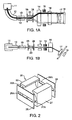
- FIG. 1A is a plan view showing a schematic structure of the single-wafer ion implantation system
- Fig. 1B is a side view of Fig. 1A .
- ions generated in an ion source 11 are extracted through an extraction electrode (not illustrated) as an ion beam (hereinafter referred to as a "beam").
- the extracted beam is analyzed by a mass analysis electromagnet device 12 so that only a necessary ion species is selected.
- the beam composed of the selected ion is shaped into a beam having a required cross-sectional shape by a beam shaper 13.
- the beam shaper 13 is formed by a Q (Quadrupole)-lens and so on.
- the beam having a regular trajectory and the shaped cross-section is deflected in a direction parallel to the sheet surface of Fig. 1A by a deflector 20 for scanning according to this invention.
- the deflector 20 has shield electrodes 25 and 26 disposed on the upstream and downstream sides thereof, respectively. The deflector 20 and the shield electrodes 25 and 26 will be described in detail later.
- the deflected beam is parallelized again by a P (Parallel)-lens 14 so as to be parallel to an axis of a deflection angle of 0 degree.
- a scan range of the beam 10 by the deflector 20 is indicated by a thick black line and broken lines.
- the thick black line and the broken lines extending from the deflector 20 can be defined as the maximum scan trajectories, respectively.
- the beam from the P-lens 14 is sent to an azimuthal energy filter 16 through one or more acceleration/deceleration electrodes 15.
- the azimuthal energy filter 16 performs analysis about energy of the beam to thereby select only an ion species with a necessary energy. As shown in Fig.
- a semiconductor wafer 17 being a to-be-implanted object is irradiated by the beam composed of only the thus selected ion species.
- the beam that is not implanted to the semiconductor wafer 17 is incident on a beam stopper 18 so that energy thereof is consumed.
- a beam line the structure from the ion source 11 to a chamber (not illustrated) where the semiconductor wafer 17 is accommodated.
- a transportation path of the beam is all maintained in a high-vacuum state and sealed from the air.
- two arrows shown adjacent to the semiconductor wafer 17 represent that the beam is deflected in directions of these arrows.
- two arrows shown adjacent to the semiconductor wafer 17 represent that the semiconductor wafer 17 is reciprocated in directions of these arrows, i.e. mechanically moved. Specifically, assuming that the beam is reciprocatingly deflected in directions of one axis, the semiconductor wafer 17 is reciprocated in directions perpendicular to such directions of one-axis.
- Fig. 2 is a perspective view showing a basic structure of the deflector according to the embodiment of this invention.
- Fig. 3 is a diagram for showing a relationship among x-, y-, and z-axes which will be explained hereinbelow with respect to the deflector according to the embodiment of this invention.
- the deflector 20 comprises a pair of deflection electrodes 21 and 22 arranged so as to confront each other with the beam interposed therebetween. Note that the arrangement shown in Fig. 2 is only one example. That is, the arrangement of the deflection electrodes 21 and 22 is not limited to the illustrated manner in which the deflection electrodes 21 and 22 are disposed so as to confront each other in the horizontal direction, i.e. in the x-axis direction in this case.
- the deflection electrodes 21 and 22 may be disposed so as to confront each other in the y-axis direction.
- the shield electrode 25 and the shield electrode 26 are disposed near the deflection electrodes 21 and 22 on their upstream and downstream sides, respectively. Note that the upstream and downstream shield electrodes 25 and 26 do not necessarily have the same shape.
- the deflection electrodes 21 and 22 are symmetrical in shape with respect to the z-axis and are disposed so that their inner electrode surfaces on the z-axis side become symmetrical with respect to the z-axis.
- concaves 21A and 22A each having a substantially circular-arc shape in cross-section are formed so as to each extend in the z-axis direction.
- the beam 10 is deflected in the z-x plane.
- the beam 10 has a flattened cross-sectional shape in which the width in the x-axis direction is greater than the width in the y-axis direction.
- the width in the y-axis direction may be referred to as a "vertical width”
- the width in the x-axis direction may be referred to as a "horizontal width”.
- the z-x plane may be referred to as a "beam deflection plane”.
- the shield electrodes 25 and 26 serve to prevent electrical fields generated by the deflection electrodes 21 and 22 from leaking to the beam trajectory outside the deflector 20.
- the shield electrodes 25 and 26 have openings 25A and 26A, respectively, and the beam passes through these openings 25A and 26A.
- Fig. 4A shows electric lines of force and electrical fields generated by conventional deflection electrodes 31 and 32 each having a planar surface on the z-axis side.
- Fig. 4B shows electric lines of force and electrical fields generated by the deflection electrodes 21 and 22 of this invention having on their surfaces on the z-axis side the concaves 21A and 22A each extending in the z-axis direction and each having the substantially circular-arc shape in cross-section.
- a shortest distance L between the confronting surfaces of the deflection electrodes 21 and 22 be defined as a distance between innermost-side ends of both electrode portions. It is assumed that, in each of Figs.
- a negative voltage -V is applied to the deflection electrode on the right side in the figure and a positive voltage +V is applied to the deflection electrode on the left side in the figure.
- lines extending in a leftward/rightward direction represent electric lines of force
- lines extending in an upward/downward direction represent equipotential lines
- thick-line arrows represent electrical fields.
- the concaves 21A and 22A are formed on the confronting surfaces on the z-axis side of the deflection electrodes 21 and 22.
- the concaves 21A and 22A are symmetrical in shape with respect to the z-axis. In this case, electric lines of force are collected near the z-axis and electrical field components in the x-axis direction become nearly uniform near the z-axis.
- the width in the x-axis (leftward/rightward) direction of each of the openings 25A and 26A is set sufficiently greater than the horizontal width of the beam so as to prevent the beam from passing near left and right edges of each of the openings 25A and 26A. This is because the electrical field is locally strengthened near the edges so that only a portion of the beam is irregularly bent,
- FIG. 5 is a diagram showing y-axis components of electrical fields near the opening of the shield electrode, herein, near the opening 25A of the upstream shield electrode 25. It may be considered that the same applies to the case of the downstream shield electrode 26.
- the electrical fields in the y-axis direction differ in a region near the shield electrode 25 and in a region sufficiently remote from the shield electrode 25. Accordingly, consideration is made about the electrical fields in the y-axis direction by dividing a region into one near the shield electrode 25 and the other region. Note that when there are a plurality of shield electrodes on each of the upstream and downstream sides of the deflection electrodes, selection is made of the shield electrode that is located closest to the deflection electrodes on each of the upstream and downstream sides thereof.
- the opening 25A of the shield electrode 25 be formed as small as possible to thereby prevent the electrical fields from leaking to the outside of the deflector 20. Accordingly, a vertical width (y-axis direction width) of the opening 25A of the shield electrode 25 is set substantially equal to the vertical width of the beam.
- the beam is directed from the front side toward the back side of the sheet of Fig. 5 , wherein the upstream shield electrode 25 is disposed on the front side of the sheet of Fig. 5 and the pair of deflection electrodes 21 and 22 are disposed behind it. If the structure of the deflection electrodes and the distribution of the electrical fields are substantially symmetrical with respect to the y-axis, the electrical fields directed as shown in Fig. 5 are generated near the opening 25A of the upstream shield electrode 25 in an instant when the positive voltage +V is applied to the left deflection electrode 22 and the negative voltage -V is applied to the right deflection electrode 21.
- Such electrical fields at the opening 25A of the shield electrode 25 vertically defocus the beam when the beam passes therethrough in a region of x ⁇ 0 (left side of z-axis), while focus the beam when the beam passes therethrough in a region of 0 ⁇ x (right side of z-axis).
- the electrical fields at the opening of the shield electrode are strong only near the opening of the shield electrode and disappear in a region slightly away from it.
- This electrical field distribution is generated under the influence of potentials of the deflection electrodes 21 and 22, and the electrical fields generated by the deflection electrodes 21 and 22 are only extremely strong near those electrodes 21 and 22. Therefore, if slightly distanced from the deflection electrodes 21 and 22, the each directionalities of the electrical field distribution hardly changes even by changing the shape of each of the deflection electrodes 21 and 22. However, the strengths of the electrical fields change. That is, in a region slightly distanced from the deflection electrodes 21 and 22, the electrical fields of the same direcfionalities are constantly generated regardless of whether the deflection electrodes are of the conventional type or the invention type.
- the electrical fields generated by the deflection electrodes 21 and 22 become dominant.
- Vertical components of the deflection electrical fields are determined by the shape of each of the concaves 21A and 22A of the deflection electrodes 21 and 22.
- the electrical field distribution becomes as shown in Fig. 6A or 6B depending on the presence/absence and shape of the concaves.
- electrical fields in the y-axis direction have the same directionality as that of the electrical fields at the opening of the shield electrode in the foregoing item i) to thereby amplify the focus/defocus of the beam in the y-axis direction.
- the deflection electrodes 21 and 22 of this invention shown in Fig. 6B are formed with the proper concaves 21A and 22A, respectively.
- electrical fields in the y-axis direction remote from the shield electrodes 25 and 26 have opposite directionalities of the electrical fields in the y-axis direction near the openings of the shield electrodes in the foregoing item i).
- Those electrical fields in the vertical direction are much weaker as compared with the electrical fields near the openings of the shield electrodes but an acting distance range thereof is long, so that the effect of focusing and defocusing become substantially equal to each other in the overall deflector 20.
- each of the concaves 21 A and 22A of the deflection electrodes 21 and 22 of this invention By determining the shape and size of each of the concaves 21 A and 22A of the deflection electrodes 21 and 22 of this invention so that the effect of the electrical fields in the vertical direction in the foregoing items i) and ii) have substantially the same magnitude to thereby cancel each other, the focus/defocus and trajectory declination of the beam in the vertical direction can be suppressed to a small level before and after passing through the deflector 20.
- each of the concaves 21A and 22A of the deflection electrodes 21 and 22 also affects the leftward/rightward (x-axis direction) beam deflection and thus is optimized by also taking it into account.
- the electrical fields having the directionalities achieved by the deflection electrodes of this invention can deflect the beam more uniformly as compared with the conventional type.
- AC voltages approximating to phase-inverted triangular waves, or sawtooth waves are applied to the two deflection electrodes 21 and 22.
- the shield electrodes 25 and 26 are provided on the upstream and downstream sides thereof, respectively, i.e. one shield electrode on each of the upstream and downstream sides. Each of the shield electrodes 25 and 26 is grounded.
- ac voltages approximating to phase-inverted triangular waves or sawtooth waves use may be made of ac voltages having the same phase and reverse polarity, ac voltages in the form of triangular waves having the same phase and reverse polarity, or ac voltages approximating to triangular waves having the same phase and reverse polarity.
- ac voltages ac rectangular wave voltages, or ac sine wave voltages having the same values, the same phase, and reverse polarity.
- DC components may be superimposed on the ac voltages.
- the scanning frequency (sweep frequency) of the deflection electrodes is set to several tens of Hz to several hundreds of Hz or more and, if circumstances require, may be set to 1 KHz or more.
- the defocus state (gradient in emittance) of the beam passing through the deflector 20 somewhat changes depending on a deflection angle
- the change in defocus state can be made relatively small and thus may be ignored depending on purpose. In that case, the beam can be deflected only by the deflector of this invention without changing the defocus state of the beam.
- the beam shaper 13 formed by the Q-lens and so on is provided as a focusing element for forcibly removing the change in defocus state of the beam.
- the Q-lens may be of an electromagnet type using quadrupole magnets or an electrical field type using quadrupole electrodes.
- a current in the case of the electromagnet type Q-lens
- a voltage in the case of the electrical field type Q-lens
- each of the deflection electrodes is not limited to that shown in Fig. 2 and various changes may be made thereto.
- the cross-sectional shape of the concave formed on each deflection electrode is not limited to the substantially circular-arc shape and may be a polygonal shape including a triangular shape, but is preferably as smooth as possible.
- each concave may have a shape that changes following z-axis coordinates.
- the surfaces of the concaves may be bent so as to be substantially parallel to the maximum scan trajectory (maximum scan angle range), respectively.
- the surfaces of the two concaves of the two deflection electrodes may form a space therebetween having a shape that widens toward the downstream side.
- the concave can be implemented by a groove.
- the concave may be implemented by a hollow cylindrical member with a hollow space defined by a cross-sectional shape of circle, polygonal, or the like, by half cutting along a center axis of the hollow cylindrical member.
- Figs. 7 to 9 show examples of concaves of deflection electrodes modified on the basis of the foregoing points.
- Fig. 7 shows an example wherein two deflection electrodes 21 and 22 like those shown in Fig. 2 are disposed so that the distance therebetween increases toward the downstream side. This is based on the viewpoint that the deflection electrodes are not required to be parallel with respect to the z-axis (center axis of the beam trajectory), i.e. the center axis of each concave does not necessarily extend in the z-axis direction. However, it is desirable that the two deflection electrodes 21 and 22 be symmetrical with respect to the z-axis.
- Fig. 8 shows an example wherein although two deflection electrodes 21 and 22 are disposed in the same manner as in Fig. 2 , the radius of the shape of each of concaves 21A-1 and 22A-1 formed on confronting surfaces on the z-axis side of the deflection electrodes 21 and 22, i.e. the radius of a circular-arc cross-sectional shape of each concave, increases toward the downstream side.
- This is based on the viewpoint that the cross-section of the concave of each deflection electrode as observed in the z-axis direction may be changed along with z-axis coordinates, However, it is desirable that the two deflection electrodes 21 and 22 be symmetrical with respect to the z-axis.
- Fig. 9 shows an example wherein each of concaves 21A-2 and 22A-2 formed on confronting surfaces on the z-axis side of two deflection electrodes 21 and 22 has a circular-arc cross-sectional shape in which the depth of the concave changes along with z-axis coordinates so as to be the shallowest at an intermediate portion in the z-axis direction.
- each concave may also be a polygonal shape including a triangular shape in any of the examples of Figs. 7 to 9 .
- the cross-sectional shape of each concave may have a circular-arc portion at a deep portion (bottom portion) and an upper and a lower planar portion as shown in Fig. 10A
- the cross-sectional shape of each concave may have a planar portion at a deep portion (bottom portion) and an upper and a lower circular-arc portion as shown in Fig. 10B .
- Each of the deflection electrodes 21 and 22 may be integrally formed or may be integrally assembled from a plurality of individual members.
- each deflection electrode is formed by individual members.
- Each of deflection electrodes 21 and 22 is composed of three individual members divided in the z-axis direction.
- the individual members are in the form of semicylindrical members 21-1 (22-1), 21-2 (22-2), and 21-3 (22-3) each obtained by splitting a hollow cylindrical member longitudinally. Further, the semicylindrical members 21-2 (22-2) and 21-3 (22-3) are formed so as to provide a shape that expands toward the downstream side at two-step angles.
- base portions 21-5 (22-5), 21-6 (22-6), and 21-7 (22-7) are integrated together by the use of joining members such as bolts.
- a plurality of shield electrodes may be provided on at least one of the upstream and downstream sides.
- it may be configured such that two shield electrodes are provided on each of the upstream and downstream sides, the electrode located closer to the deflection electrodes is applied with a dc voltage of about -1 kV to -2kV so as to serve as a suppression electrode (electron suppression electrode), while the electrode located farther from the deflection electrodes is grounded so as to serve as a ground electrode.
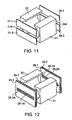
- Figs. 11 and 12 show examples of shield electrodes modified on the basis of the foregoing points.
- Fig. 11 shows an example wherein, instead of the shield electrodes each having the opening, two electrode plates 27-1 and 27-2 are arranged side by side with a distance defined therebetween so as to form a beam passing opening 27A and likewise two electrode plates 28-1 and 28-2 are arranged side by side with a distance defined therebetween so as to form a beam passing opening 28A.
- the same voltage is applied to the electrode plates 27-1 and 27-2 and the same voltage is also applied to the electrode plates 28-1 and 28-2.
- Fig. 12 shows another embodiment wherein two shield electrodes 25-1 and 25-2 are disposed on the upstream side of the deflection electrodes 21 and 22 and likewise two shield electrodes 26-1 and 26-2 are disposed on the downstream side thereof. It is preferable that each of the shield electrodes can be independently applied with a voltage. As described above, the electrode located closer to the deflection electrodes may be applied with a dc voltage of about -1 kV to -2kV so as to serve as a suppression electrode, while the electrode located farther from the deflection electrodes may be grounded so as to serve as a ground electrode.
- each opening 25-1A and 25-2A of the shield electrodes 25-1 and 25-2 are preferably equal to each other but may be different from each other and likewise the sizes of openings 26-1A and 26-2A of the shield electrodes 26-1 and 26-2 are preferably equal to each other but may be different from each other.
- each opening may have a shape, other than the substantially rectangular shape, in which upper and lower edges of the opening are curved so that a center portion of the opening becomes narrower as compared with both end portions thereof. In this case, a vertical defocus/focus action against the beam can be adjusted to some degree.
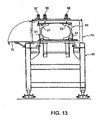
- Fig. 13 is a front cross-sectional view, as seen from the downstream side, of a structure wherein the deflector is detachably mounted midway in the beam line.
- Fig. 14 is a transverse sectional view, as seen from above, of the main part of the structure shown in Fig. 13 .
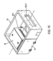
- Fig. 15 is a perspective view showing a detachable structure for the deflector.
- Fig. 16 is a perspective view showing the state where the detachable structure for the deflector is on the way to detach the deflector.
- the pair of deflection electrodes 21 and 22 and the shield electrodes 25 and 26 mounted near the deflection electrodes 21 and 22 on the upstream and downstream sides thereof are accommodated and disposed within a housing 50.
- the housing 50 has an upstream wall and a downstream wall.
- the upstream wall of the housing 50 is formed, at its portion corresponding to the opening 25A of the shield electrode 25, with an upstream opening (not illustrated), while the downstream wall of the housing 50 is formed, at its portion corresponding to the opening 26A of the shield electrode 26, with a downstream opening 52A which is slightly larger than the opening 26A.
- Connection between the deflection electrodes and a power supply and connection between the shield electrodes and a power supply are realized by a feedthrough structure.
- the housing 50 has a lateral side where terminals 53 and 54 are provided for connecting the dc power supply to the shield electrodes 25 and 26.
- the housing 50 has a top side where there are provided terminals 55 and 56 for connecting the power supply to the deflection electrodes 21 and 22 and a terminal 57 for grounding.
- grips 51 On two lateral sides, parallel to the center axis of the beam trajectory, of the housing 50 are provided grips 51 which are used for attaching, detaching, or carrying the housing 50.
- symbol 70A-3 denotes an outlet for evacuation carried out for increasing the degree of vacuum within the deflector and the outlet 70A-3 is connected to an evacuator (not illustrated).
- the housing 50 is slidably disposed in a beam guide box 70 fixedly mounted on a rack 60.
- the beam guide box 70 is sufficiently larger than the housing 50.
- two guide rails 71 are disposed for allowing the housing 50 to be slidable therealong.
- Each guide rail 71 extends in a direction perpendicular to the center axis of the beam trajectory.
- the beam guide box 70 has a lateral side that can be opened and closed by a door 72 near one end of each guide rail 71. With this arrangement, the housing 50 can be easily taken out from the beam guide box 70 at the time of maintenance and checkout.
- the beam guide box 70 has an upstream wall and a downstream wall that are formed, at their portions corresponding to the upstream opening and the downstream opening 52A of the housing 50, with openings 70A-1 and 70A-2, respectively.
- the opening 70A-1 does not need to be large because the incident beam trajectory hardly changes.
- the opening 70A-2 is required to be larger than the opening 52A because the outgoing beam is deflected.
- Lead wires (not illustrated) are connected to the terminals 53 to 57 but are detached when attaching or detaching the housing 50.
- the housing 50 is configured that it is capable of freely putting on and taking off for the beam line in a midway thereof.
- the scan range is wide (e.g. scan angle: 13.5 degree).
- the distance L between the deflection electrodes is large (e.g. several hundreds of mm or more).
- the beam profile is not distorted even when the scan angle is large.
- the deflection electrodes can be designed so that a change in profile of the beam is made as small as possible and orderly with respect to the deflection angle.
- the suppression electrode and the ground electrode are disposed on each of the upstream and downstream sides of the deflection electrodes.
- each of the openings of the suppression and ground electrodes is formed into the shape that is large in the horizontal-width direction of the beam while only slightly wider than the vertical width of the beam in the vertical-width direction of the beam so as to well suppress the electrical field, thereby having the rectangular shape with a large aspect ratio.
- the suppression and ground electrodes cause the electrical field to be weak in the large-width direction and enable deflection scanning of a beam with a high current density of about 10mA/cm 2 without causing defocus thereof.
- the size of the overall beam processing system can be the same as the conventional size by the use of the practical and compact deflector.
- the operation attendant upon maintenance and checkout can be facilitated by allowing the deflector to be attachable and detachable with respect to the beam line.
- the deflector according to this invention is suitable for the whole range of beam processing systems that deflect a beam having a relatively large diameter or a beam having a flattened shape, such as an oval shape, in cross-section.
Landscapes
- Chemical & Material Sciences (AREA)
- Analytical Chemistry (AREA)
- Electron Beam Exposure (AREA)
- Physical Vapour Deposition (AREA)
Claims (29)
- Dispositif comprenant un formeur de faisceau (13) et un déflecteur de faisceau (20) pour dévier un faisceau de particules chargées (10) par rapport à une trajectoire normale dans un espace sous vide, pour en modifier la trajectoire, le déflecteur de faisceau comportant une paire d'électrodes de déflexion (21, 22) disposées pour avoir chacune, par l'intermédiaire de d'électrodes intérieures, des parties concaves symétriques (21A, 21A-1, 21A-2, 22A, 22A-1, 22A-2), s'étendant dans la direction de la trajectoire du faisceau, le faisceau de particules chargées passant dans l'espace entre la paire d'électrodes de déflexion générant un champ électrique uniforme pour dévier le faisceau, et un ensemble d'électrodes-écran (25-1, 25-2, 26-1, 26-2), ayant chacune une ouverture (25-1A, 25-2A, 26-1A, 26-2A), permettant le passage du faisceau et disposées au voisinage de la paire d'électrodes de déflexion, du côté amont et du côté aval,
caractérisé en ce que
le faisceau de particules chargées est formé avec une section aplatie telle qu'une section ovale, par le dispositif formeur de faisceau, réalisé pour mettre en forme un faisceau de particules et ayant de préférence une lentille à quadripôle, la formé de la section aplatie telle qu'une section ovale avant une largeur, dans la direction parallèle à la direction de mise en forme de la paire d'électrodes de déflexion, plus grande que la largeur mesurée perpendiculairement à la direction de mise en forme, et le champ électrique généré par la paire d'électrodes de déflexion est réparti uniformément pour le faisceau de particules chargées à section aplatie qu'une section ovale soit dévié pratiquement selon le même de déflexion en tout endroit, par rapport à sa section. - Dispositif selon la revendication 1,
en ce que
la forme de la section de chaque partie concave se compose d'une forme essentiellement concave en arc de cercle ou d'une forme concave polygonale. - Dispositif selon la revendication 1 ou 2,
caractérisé en ce que
la section de chaque partie concave varie de manière linéaire ou par paliers suivant l'axe central de la trajectoire du faisceau. - Dispositif selon les revendications 1 à 3,
caractérisé en ce que
les surfaces de l'électrode intérieure, dans la direction de mise en forme de la paire d'électrodes de déflexion, divergent le long des trajectoires de balayage maximum par rapport à l'axe de la trajectoire du faisceau pour être pratiquement parallèles au maximum des trajectoires balayées. - dispositif selon les revendications 1 à 4,
caractérisé en ce que
la paire d'électrodes de déflexion est prévue pour appliquer des tensions alternatives de même fréquence et de polarité inversée. - Dispositif selon les revendications 1 à 4,
caractérisé en ce que
la paire d'électrodes de déflexion peut recevoir des tensions alternatives de même niveau, de même fréquence et de polarités opposées. - Dispositif selon la revendication 5 ou 6,
caractérisé en ce que
les composantes continues sont combinées aux tensions alternatives. - Dispositif selon les revendications 1 à 7,
caractérisé en ce que
chacune des paires d'électrodes de déflexion est formée d'un ensemble d'éléments individuels (21-1, 21-2, 21-3, 22-1, 22-2, 22-3) divisés dans la direction de l'axe central de la trajectoire du faisceau. - Système d'implantation ionique comportant un dispositif comprenant un formeur de faisceaux (13) et un déflecteur de faisceaux selon les revendications 1 à 8.
- Procédé de déflexion d'un faisceau pour dévier un faisceau de particules chargées (10) d'une trajectoire normale dans un espace vide, de manière à en modifier la trajectoire et comprenant les étapes suivantes :- préparation d'une paire d'électrodes de déflexion (21, 22) disposées pour s'adapter l'une à l'autre par l'intermédiaire des surfaces d'électrodes internes (21A, 21A-1, 21A-2, 22A, 22A-1, 22A-2), avec une région concave disposée symétriquement et s'étendant dans la direction de l'axe central de la trajectoire du faisceau en appliquant un champ électrique uniforme, généré par la paire d'électrodes de déflexion, au faisceau de particules chargées, passant dans l'intervalle entre la paire d'électrodes de déflexion de manière à dévier le faisceau,- préparation d'un ensemble d'électrodes-écran (25-1, 25-2, 26-1, 26-2) disposées au voisinage de la paire d'électrodes de déflexion sur le côté amont et le côté aval, respectif, chacun des ensembles d'électrodes-écran ayant une ouverture permettant le passage d'un faisceau (25-1A, 25-2A, 26-1A, 26-2A),caractérisé en ce que
le procédé comprend en outre les étapes suivantes :- mise en forme du faisceau de particules chargées une section aplatie telle qu'une section ovale par un formeur de faisceau ayant une lentille quadripôle, la forme de la section aplatie telle qu'une section ovale avec une largeur parallèle à la direction de en forme de la paire d'électrodes de déflexion étant supérieure à la largeur perpendiculaire à la direction de conformation, et- répartition uniforme du champ électrique généré par la paire d'électrodes de déflexion de façon que les particules chargées mises en forme avec une section transversale telle qu'une section ovale aplatie sont déviées pratiquement la même direction angulaire dans les parties, par rapport à la section. - de déflexion d'un faisceau selon la revendication 10,
caractérisé en ce que
la paire d'électrodes de déflexion, dont les formes sont disposées pour former des champs électriques de manière à uniformiser la distribution du champ électrique en largeur dans la direction horizontale du faisceau, devient uniforme dans toutes les positions du faisceau, dans la direction d'avancée entre la paire d'électrodes de déflexion. - Procédé de déflexion d'un faisceau selon la revendication 10,
caractérisé en ce qu'
il comprend en outre les étapes suivantes :- faire entrer le faisceau de particules chargées par le côté entrée de la paire d'électrodes de déflexion du moyen de déflexion de faisceau pour le balayage, ce faisceau de particules chargées ayant une section ovale dont la largeur horizontale, parallèle à la direction de conformation de la paire d'électrodes de déflexion, est supérieure à la longueur verticale du faisceau ovale, perpendiculairement à la direction de mise en forme et- appliquer un effet de déflexion périodique pour balayer la direction de mise en forme électrodes de déflexion. - Procédé de déflexion d'un faisceau selon la revendication 12,
caractérisé en ce que
l'espace compris entre la paire d'électrodes de déflexion et la variation du profil de faisceau est limité par rapport à l'angle de déflexion. - Procédé de déflexion d'un faisceau selon la revendication 10,
caractérisé en outre par les étapes suivantes :- déflexion du faisceau de particules chargées dans l'une des directions de balayage en utilisant une paire d'électrodes de déflexion, et- déplacement du substrat (17) destiné à être implanté par le faisceau de particules chargées, dans une direction perpendiculaire à l'une des directions de balayage, au cours de l'implantation ionique. - Procédé d'implantation ionique selon les revendications précédentes 10 à 14.
- Dispositif selon la revendication 1,
caractérisé en ce que
pour avoir une zone de champ électrique uniforme par les électrodes de déflexion, le côté entrée de la paire d'électrodes de déflexion a un écartement d'électrodes entre les extrémités les plus à l'intérieur des parties mises en forme et les distances entre les électrodes sont supérieures à la largeur horizontale du faisceau incident chargé de particules. - Dispositif selon la revendication 16,
caractérisé en ce que
chacune des électrodes de champ reçoit une tension fixe ou une tension variable. - Dispositif selon la revendication 16,
caractérisé en ce que
les deux électrodes de champ (25-1, 25-2, 26-1, 26-2) sont disposées chacune sur le côté amont et le côté aval de la paire d'électrodes de déflexion, l'une des deux électrodes de déflexion (25-1) du côté amont est plus proche de la paire des électrodes de déflexion et l'une des deux électrodes-écran (26-1) du côté aval, située plus près de la paire d'électrodes de déflexion, et elles sont réparties pour recevoir une tension alternative d'environ 1 kV à 2 kV et servir d'électrodes de suppression d'électrons et l'autre des deux électrodes-écran (25-2) du côté amont et l'autre des deux électrodes (26-2) du côté aval sont mises à la masse pour servir ainsi d'électrodes de mise à la masse. - Dispositif selon la revendication 18,
caractérise en ce que
chacune des ouvertures (25-1A, 26-1A, 25-2A, 26-2A) des électrodes de suppression et de masse ont une forme rectangulaire et donnent un faisceau horizontal important de largeur supérieure à la largeur verticale pour la suppression du champ électrique. - Dispositif selon les revendications 17 à 19,
caracterisé en ce que
l'ouverture (25A,25-1A, 25-2A, 26A, 26-1A, 27A, 29A) de chacune des électrodes formant écran sur le côté amont et le côté aval est configurée de façon que sa largeur, dans la direction du faisceau horizontal, soit supérieure à celle du faisceau horizontal pour éviter la charge des particules du faisceau passant près des bords de l'ouverture dans la direction de la largeur horizontale du faisceau. - Dispositif selon la revendication 16,
caractérisé en ce que
la forme et les dimensions de chacune des parties concaves de la paire d'électrodes sont déterminées de façon que les champs électriques, dans la direction perpendiculaire plane de déflexion du faisceau à proximité des électrodes de champ et les champs électriques dans la direction perpendiculaire au plan de déflexion du faisceau émis par le détecteur de faisceau pour le balayage, se compensent l'un l'autre et ainsi on réduit la focalisation/défocalisation et la déclinaison de trajectoire du faisceau à particules chargées dans la direction perpendiculaire au plan de déflexion du faisceau avant et après le passage du déflecteur de faisceau. - Dispositif selon la revendication 16, réalisé de façon générer un champ électrique dans la direction perpendiculaire au plan de déflexion du faisceau dans la partie centrale du déflecteur de faisceau pour que le balayage soit plus fort que les champs électriques dans les autres régions.
- Dispositif les revendications 16 à 22,
caractérisé en ce que
chacune des paires d'électrodes de déflexion est formée par un ensemble d'éléments individuels (21-1, 21-2, 21-3, 22-1, 22-2, 22-3) divisé dans la direction de l'axe central de la trajectoire du faisceau. - Système d'implantation ionique comportant un montage de mise es forme de faisceau (13) et un montage de déflexion de faisceau (20) selon une ou plusieurs des revendications 16 à 23.
- Système d'implantation ionique selon la revendication 9 ou 24,
caractérisé en ce que
la paire d'électrodes de déflexion est disposée dans un boîtier (50) muni d'ouvertures (52A) pour le passage du faisceau et l'électrode est configurée pour être montée librement et être démontée de la ligne du faisceau au milieu de cette ligne. - Système d'implantation ionique selon la revendication 25,
caractérisé en ce qu'
un râtelier (60) est prévu à mi-chemin de la ligne de faisceau et une boîte de guidage de faisceau (70) ayant des ouvertures de passage de faisceau (70A-1, 70A-2), plus grandes que le boîtier, est montée sur le râtelier, le boîtier étant mobile le long d'un élément de rail (72) prévu dans la boîte de guidage de faisceau de façon que le boîtier puisse en être logé et extrait. - Système d'implantation ionique selon la revendication 26,
caractérisé en ce que
le rail s'étend dans une direction perpendiculaire à la direction d'extension de la ligne de faisceau et une porté (72), prévue sur un côté à proximité d'une extrémité du rail, permet au boîtier d'être logé dans la boîte de guidage de faisceau. - Système d'implantation ionique selon les revendications 25 à 27,
caractérisé en ce que
le boîtier comporte un ensemble de bornes (53, 54, 55, 56, 57) ayant une structure de réaction pour réaliser la connexion entre au moins la paire d'électrodes de déflexion et l'alimentation électrique. - Système d'implantation ionique selon les revendications 25 à 28,
caractérisé en ce que
la sortie (70A-3), reliée à un évacuateur, est prévue dans le boîtier.
Applications Claiming Priority (1)
| Application Number | Priority Date | Filing Date | Title |
|---|---|---|---|
| JP2004347298A JP5214090B2 (ja) | 2004-11-30 | 2004-11-30 | ビーム偏向走査方法及びビーム偏向走査装置並びにイオン注入方法及びイオン注入装置 |
Publications (3)
| Publication Number | Publication Date |
|---|---|
| EP1670027A2 EP1670027A2 (fr) | 2006-06-14 |
| EP1670027A3 EP1670027A3 (fr) | 2006-06-21 |
| EP1670027B1 true EP1670027B1 (fr) | 2009-03-25 |
Family
ID=34941519
Family Applications (1)
| Application Number | Title | Priority Date | Filing Date |
|---|---|---|---|
| EP05253337A Expired - Lifetime EP1670027B1 (fr) | 2004-11-30 | 2005-05-31 | Arrangement de dispositif de dispositif de former et de déflection d'un faisceau de particules, procédé de déflection d'un faisceau de particules, procédé d'implantation d'ions et système d'implantation d'ions |
Country Status (6)
| Country | Link |
|---|---|
| US (1) | US7138641B2 (fr) |
| EP (1) | EP1670027B1 (fr) |
| JP (1) | JP5214090B2 (fr) |
| KR (1) | KR101119073B1 (fr) |
| DE (1) | DE602005013475D1 (fr) |
| TW (1) | TWI391976B (fr) |
Families Citing this family (22)
| Publication number | Priority date | Publication date | Assignee | Title |
|---|---|---|---|---|
| JP5100963B2 (ja) * | 2004-11-30 | 2012-12-19 | 株式会社Sen | ビーム照射装置 |
| JP4828305B2 (ja) | 2006-05-30 | 2011-11-30 | 株式会社Sen | 静電式ビーム偏向走査装置及びビーム偏向走査方法 |
| EP1883094B1 (fr) * | 2006-07-24 | 2012-05-02 | ICT, Integrated Circuit Testing Gesellschaft für Halbleiterprüftechnik mbH | Appareil à faisceau de particules et procédé pour l'examen d'un échantillon |
| US20080099696A1 (en) * | 2006-10-31 | 2008-05-01 | Applied Materials, Inc. | Shaped apertures in an ion implanter |
| JP5329050B2 (ja) | 2007-04-20 | 2013-10-30 | 株式会社Sen | ビーム処理装置 |
| TWI497557B (zh) * | 2009-04-29 | 2015-08-21 | Mapper Lithography Ip Bv | 包含靜電偏轉器的帶電粒子光學系統 |
| JP6053919B2 (ja) * | 2012-05-31 | 2016-12-27 | シーメンス アクチエンゲゼルシヤフトSiemens Aktiengesellschaft | 荷電粒子を偏向させる偏向板および偏向装置 |
| US8841631B1 (en) * | 2013-06-26 | 2014-09-23 | Varian Semiconductor Equipment Associates, Inc. | Apparatus and techniques for controlling ion angular spread |
| US9892931B2 (en) * | 2013-10-14 | 2018-02-13 | Taiwan Semiconductor Manufacturing Company Ltd. | Semiconductor manufacturing apparatus and method thereof |
| US9711318B2 (en) * | 2013-12-20 | 2017-07-18 | Nicholas R. White | Ribbon beam ion source of arbitrary length |
| JP6257411B2 (ja) * | 2014-03-27 | 2018-01-10 | 住友重機械イオンテクノロジー株式会社 | イオン注入装置、最終エネルギーフィルター、及びイオン注入方法 |
| JP6161571B2 (ja) * | 2014-05-26 | 2017-07-12 | 住友重機械イオンテクノロジー株式会社 | イオン注入装置 |
| JP6278835B2 (ja) | 2014-05-26 | 2018-02-14 | 住友重機械イオンテクノロジー株式会社 | イオン注入装置 |
| US9805908B2 (en) * | 2015-02-18 | 2017-10-31 | Integrated Circuit Testing Gesellschaft für Halbleiterprüftechnik mbH | Signal charged particle deflection device, signal charged particle detection system, charged particle beam device and method of detection of a signal charged particle beam |
| CN109767971B (zh) * | 2019-03-08 | 2024-08-13 | 昆山禾信质谱技术有限公司 | 二维离子束偏转装置 |
| EP4000355A4 (fr) | 2019-07-19 | 2023-06-28 | Phoenix, LLC | Déflexion de jet de gaz dans des systèmes sous pression |
| CN111105971B (zh) * | 2019-12-06 | 2022-06-14 | 中国科学院微电子研究所 | 一种离子注入装置 |
| CN111385958A (zh) * | 2020-04-07 | 2020-07-07 | 哈尔滨工业大学 | 一种新型弧形斜边静电偏转板及粒子加速器斩波器 |
| CN113082550B (zh) * | 2021-03-26 | 2022-12-06 | 中以康联国际医疗科技有限公司 | 粒子射束监控方法及粒子射束治疗装置 |
| JP7647271B2 (ja) * | 2021-04-13 | 2025-03-18 | 株式会社ニューフレアテクノロジー | 荷電粒子ビーム描画装置 |
| CN115052408B (zh) * | 2022-07-13 | 2024-09-27 | 中国原子能科学研究院 | 具有横向聚焦力的v型截面加速器螺旋偏转板设计方法 |
| CN115413106B (zh) * | 2022-07-13 | 2025-01-28 | 中国原子能科学研究院 | 具有横向聚焦力的倾斜截面加速器螺旋偏转板设计方法 |
Citations (2)
| Publication number | Priority date | Publication date | Assignee | Title |
|---|---|---|---|---|
| US4254340A (en) * | 1977-12-23 | 1981-03-03 | Agence Nationale De Valorisation De La Recherche (Anvar) | High current ion implanter |
| WO2001031679A1 (fr) * | 1999-10-22 | 2001-05-03 | Varian Semiconductor Equipment Associates, Inc. | Appareils a balayage a faisceau ionique a large spectre |
Family Cites Families (17)
| Publication number | Priority date | Publication date | Assignee | Title |
|---|---|---|---|---|
| JPS61142646A (ja) * | 1984-12-14 | 1986-06-30 | Nippon Telegr & Teleph Corp <Ntt> | 荷電粒子ビ−ム用集束偏向装置 |
| JP2739078B2 (ja) * | 1988-05-21 | 1998-04-08 | 東京エレクトロン株式会社 | イオン注入装置 |
| US5041731A (en) * | 1989-01-20 | 1991-08-20 | Fujitsu Limited | Deflection compensating device for converging lens |
| JPH02260359A (ja) * | 1989-03-31 | 1990-10-23 | Ulvac Corp | 平行走査用イオン注入装置 |
| JP3380652B2 (ja) * | 1995-05-26 | 2003-02-24 | 東京エレクトロン株式会社 | 処理装置 |
| JPH09246145A (ja) * | 1996-03-04 | 1997-09-19 | Hitachi Ltd | 電子ビーム描画方法および描画装置およびこれを用いた半導体集積回路装置 |
| US5981961A (en) * | 1996-03-15 | 1999-11-09 | Applied Materials, Inc. | Apparatus and method for improved scanning efficiency in an ion implanter |
| JPH1064470A (ja) * | 1996-08-12 | 1998-03-06 | Nissin Electric Co Ltd | イオン注入装置の走査装置 |
| US6075249A (en) * | 1998-06-19 | 2000-06-13 | Varian Semiconductor Equipment Associates, Inc. | Methods and apparatus for scanning and focusing an ion beam |
| JP2001160500A (ja) * | 1999-12-01 | 2001-06-12 | Nissin High Voltage Co Ltd | タンデム加速器及びタンデム加速器用タンク |
| JP5072163B2 (ja) * | 2000-05-15 | 2012-11-14 | バリアン・セミコンダクター・エクイップメント・アソシエイツ・インコーポレイテッド | 高能率走査イオン注入器 |
| EP2587515A1 (fr) * | 2000-06-27 | 2013-05-01 | Ebara Corporation | Système d'inspection par faisceau de particules chargées et procédé de fabrication de dispositifs utilisant ledit système |
| WO2002013227A1 (fr) * | 2000-07-27 | 2002-02-14 | Ebara Corporation | Appareil d'analyse a faisceau plan |
| US6855929B2 (en) * | 2000-12-01 | 2005-02-15 | Ebara Corporation | Apparatus for inspection with electron beam, method for operating same, and method for manufacturing semiconductor device using former |
| JP2003031173A (ja) | 2001-07-11 | 2003-01-31 | Ebara Corp | 荷電粒子ビーム制御装置及びそれを用いた荷電粒子ビーム光学装置、ならびに荷電粒子ビーム欠陥検査装置 |
| US6777696B1 (en) * | 2003-02-21 | 2004-08-17 | Axcelis Technologies, Inc. | Deflecting acceleration/deceleration gap |
| GB2408143B (en) * | 2003-10-20 | 2006-11-15 | Ims Nanofabrication Gmbh | Charged-particle multi-beam exposure apparatus |
-
2004
- 2004-11-30 JP JP2004347298A patent/JP5214090B2/ja not_active Expired - Fee Related
-
2005
- 2005-05-31 TW TW094117899A patent/TWI391976B/zh not_active IP Right Cessation
- 2005-05-31 EP EP05253337A patent/EP1670027B1/fr not_active Expired - Lifetime
- 2005-05-31 US US11/139,490 patent/US7138641B2/en not_active Expired - Lifetime
- 2005-05-31 DE DE602005013475T patent/DE602005013475D1/de not_active Expired - Lifetime
- 2005-06-08 KR KR1020050048856A patent/KR101119073B1/ko not_active Expired - Fee Related
Patent Citations (2)
| Publication number | Priority date | Publication date | Assignee | Title |
|---|---|---|---|---|
| US4254340A (en) * | 1977-12-23 | 1981-03-03 | Agence Nationale De Valorisation De La Recherche (Anvar) | High current ion implanter |
| WO2001031679A1 (fr) * | 1999-10-22 | 2001-05-03 | Varian Semiconductor Equipment Associates, Inc. | Appareils a balayage a faisceau ionique a large spectre |
Also Published As
| Publication number | Publication date |
|---|---|
| TW200618025A (en) | 2006-06-01 |
| KR20060060531A (ko) | 2006-06-05 |
| TWI391976B (zh) | 2013-04-01 |
| JP5214090B2 (ja) | 2013-06-19 |
| JP2006156236A (ja) | 2006-06-15 |
| EP1670027A2 (fr) | 2006-06-14 |
| US7138641B2 (en) | 2006-11-21 |
| DE602005013475D1 (de) | 2009-05-07 |
| EP1670027A3 (fr) | 2006-06-21 |
| KR101119073B1 (ko) | 2012-03-15 |
| US20060113490A1 (en) | 2006-06-01 |
Similar Documents
| Publication | Publication Date | Title |
|---|---|---|
| EP1670027B1 (fr) | Arrangement de dispositif de dispositif de former et de déflection d'un faisceau de particules, procédé de déflection d'un faisceau de particules, procédé d'implantation d'ions et système d'implantation d'ions | |
| JP3713683B2 (ja) | イオンビームの質量分離フィルタとその質量分離方法及びこれを使用するイオン源 | |
| JP6281257B2 (ja) | リボンイオンビームのエネルギーを変更するためのシステム | |
| TWI391977B (zh) | 使用離子束之照射系統、增進照射準確度之方法及校正射束軌跡偏差之方法 | |
| EP1983549B1 (fr) | Appareil de traitement par faisceau | |
| EP1981058B1 (fr) | Appareil d'implantation ionique et procédé d'implantation ionique | |
| US7755067B2 (en) | Ion implantation apparatus and method of converging/shaping ion beam used therefor | |
| TWI375249B (en) | Irradiation system with ion beam and automatic tuning system | |
| GB2378313A (en) | Reducing space charge effects in ion beams using cusp-type magnetic fields | |
| JP2019537816A (ja) | イオン源 | |
| US9165744B2 (en) | Apparatus for treating ion beam | |
| US7276711B2 (en) | Beam space-charge compensation device and ion implantation system having the same | |
| US7304319B2 (en) | Wafer charge compensation device and ion implantation system having the same | |
| JP6428726B2 (ja) | イオン注入システム | |
| US9502213B2 (en) | Ion beam line | |
| TW202503812A (zh) | 離子束處理裝置、離子束處理系統及離子束處理方法 |
Legal Events
| Date | Code | Title | Description |
|---|---|---|---|
| PUAI | Public reference made under article 153(3) epc to a published international application that has entered the european phase |
Free format text: ORIGINAL CODE: 0009012 |
|
| PUAL | Search report despatched |
Free format text: ORIGINAL CODE: 0009013 |
|
| AK | Designated contracting states |
Kind code of ref document: A2 Designated state(s): AT BE BG CH CY CZ DE DK EE ES FI FR GB GR HU IE IS IT LI LT LU MC NL PL PT RO SE SI SK TR |
|
| AX | Request for extension of the european patent |
Extension state: AL BA HR LV MK YU |
|
| AK | Designated contracting states |
Kind code of ref document: A3 Designated state(s): AT BE BG CH CY CZ DE DK EE ES FI FR GB GR HU IE IS IT LI LT LU MC NL PL PT RO SE SI SK TR |
|
| AX | Request for extension of the european patent |
Extension state: AL BA HR LV MK YU |
|
| 17P | Request for examination filed |
Effective date: 20061206 |
|
| 17Q | First examination report despatched |
Effective date: 20070125 |
|
| AKX | Designation fees paid |
Designated state(s): DE FR GB |
|
| RTI1 | Title (correction) |
Free format text: ARRANGEMENT OF BEAM SHAPER AND BEAM DEFLECTOR, BEAM DEFLECTING METHOD, ION IMPLANTATION METHOD, AND ION IMPLANTATION SYSTEM |
|
| GRAP | Despatch of communication of intention to grant a patent |
Free format text: ORIGINAL CODE: EPIDOSNIGR1 |
|
| GRAS | Grant fee paid |
Free format text: ORIGINAL CODE: EPIDOSNIGR3 |
|
| RAP1 | Party data changed (applicant data changed or rights of an application transferred) |
Owner name: SEN CORPORATION, AN SHI AND AXCELIS COMPANY |
|
| GRAA | (expected) grant |
Free format text: ORIGINAL CODE: 0009210 |
|
| AK | Designated contracting states |
Kind code of ref document: B1 Designated state(s): DE FR GB |
|
| REG | Reference to a national code |
Ref country code: GB Ref legal event code: FG4D |
|
| REF | Corresponds to: |
Ref document number: 602005013475 Country of ref document: DE Date of ref document: 20090507 Kind code of ref document: P |
|
| PLBE | No opposition filed within time limit |
Free format text: ORIGINAL CODE: 0009261 |
|
| STAA | Information on the status of an ep patent application or granted ep patent |
Free format text: STATUS: NO OPPOSITION FILED WITHIN TIME LIMIT |
|
| 26N | No opposition filed |
Effective date: 20091229 |
|
| PGFP | Annual fee paid to national office [announced via postgrant information from national office to epo] |
Ref country code: DE Payment date: 20120531 Year of fee payment: 8 |
|
| PGFP | Annual fee paid to national office [announced via postgrant information from national office to epo] |
Ref country code: GB Payment date: 20120606 Year of fee payment: 8 Ref country code: FR Payment date: 20120619 Year of fee payment: 8 |
|
| GBPC | Gb: european patent ceased through non-payment of renewal fee |
Effective date: 20130531 |
|
| PG25 | Lapsed in a contracting state [announced via postgrant information from national office to epo] |
Ref country code: DE Free format text: LAPSE BECAUSE OF NON-PAYMENT OF DUE FEES Effective date: 20131203 |
|
| REG | Reference to a national code |
Ref country code: DE Ref legal event code: R119 Ref document number: 602005013475 Country of ref document: DE Effective date: 20131203 |
|
| REG | Reference to a national code |
Ref country code: FR Ref legal event code: ST Effective date: 20140131 |
|
| PG25 | Lapsed in a contracting state [announced via postgrant information from national office to epo] |
Ref country code: GB Free format text: LAPSE BECAUSE OF NON-PAYMENT OF DUE FEES Effective date: 20130531 |
|
| PG25 | Lapsed in a contracting state [announced via postgrant information from national office to epo] |
Ref country code: FR Free format text: LAPSE BECAUSE OF NON-PAYMENT OF DUE FEES Effective date: 20130531 |