EP1670056B1 - Leistungshalbleitermodul mit Hilfsanschluss - Google Patents
Leistungshalbleitermodul mit Hilfsanschluss Download PDFInfo
- Publication number
- EP1670056B1 EP1670056B1 EP05025505.8A EP05025505A EP1670056B1 EP 1670056 B1 EP1670056 B1 EP 1670056B1 EP 05025505 A EP05025505 A EP 05025505A EP 1670056 B1 EP1670056 B1 EP 1670056B1
- Authority
- EP
- European Patent Office
- Prior art keywords
- power semiconductor
- contact
- terminal
- connection
- semiconductor module
- Prior art date
- Legal status (The legal status is an assumption and is not a legal conclusion. Google has not performed a legal analysis and makes no representation as to the accuracy of the status listed.)
- Expired - Lifetime
Links
Images


Classifications
-
- H—ELECTRICITY
- H10—SEMICONDUCTOR DEVICES; ELECTRIC SOLID-STATE DEVICES NOT OTHERWISE PROVIDED FOR
- H10P—GENERIC PROCESSES OR APPARATUS FOR THE MANUFACTURE OR TREATMENT OF DEVICES COVERED BY CLASS H10
- H10P95/00—Generic processes or apparatus for manufacture or treatments not covered by the other groups of this subclass
-
- H—ELECTRICITY
- H10—SEMICONDUCTOR DEVICES; ELECTRIC SOLID-STATE DEVICES NOT OTHERWISE PROVIDED FOR
- H10W—GENERIC PACKAGES, INTERCONNECTIONS, CONNECTORS OR OTHER CONSTRUCTIONAL DETAILS OF DEVICES COVERED BY CLASS H10
- H10W76/00—Containers; Fillings or auxiliary members therefor; Seals
- H10W76/10—Containers or parts thereof
- H10W76/12—Containers or parts thereof characterised by their shape
- H10W76/13—Containers comprising a conductive base serving as an interconnection
-
- H—ELECTRICITY
- H10—SEMICONDUCTOR DEVICES; ELECTRIC SOLID-STATE DEVICES NOT OTHERWISE PROVIDED FOR
- H10W—GENERIC PACKAGES, INTERCONNECTIONS, CONNECTORS OR OTHER CONSTRUCTIONAL DETAILS OF DEVICES COVERED BY CLASS H10
- H10W76/00—Containers; Fillings or auxiliary members therefor; Seals
- H10W76/10—Containers or parts thereof
- H10W76/12—Containers or parts thereof characterised by their shape
- H10W76/13—Containers comprising a conductive base serving as an interconnection
- H10W76/138—Containers comprising a conductive base serving as an interconnection having another interconnection being formed by a cover plate parallel to the conductive base, e.g. sandwich type
Definitions
- a power semiconductor module is proposed with a secure internal connection of the auxiliary connection contact of a power semiconductor component arranged therein with an outer connection element.
- Various embodiments of power semiconductor modules are known, for example with a substrate having a plurality of power semiconductor components arranged thereon and a plastic housing enclosing these. In part, such power semiconductor modules also have metallic base plates. Also well known are disc cells with a hermetically sealed housing and usually only a single semiconductor device in its interior. The proposed embodiments are suitable for all types of power semiconductor modules, but have special advantages especially for disk cells.
- disc cell As it has been known for a long time prior art and is produced in many ways.
- Such disc cells are as exemplified in the DE 101 32 169 A1 seen from a cylindrical lsolierstoff Archives as a housing.
- at least one power semiconductor component for example a power diode, a power transistor or a power thyristor.
- the invention relates primarily to those disc cells with controlled power semiconductor devices in their interior.
- auxiliary connection is therefore understood to mean mainly the connection of the control connection of the power semiconductor component. Likewise, however, auxiliary emitter connections or connections for sensors integrated in the power semiconductor module are also subsumed under the term.
- the auxiliary terminals of a disc cell are configured in the prior art as a contact means for connecting the auxiliary terminal with the An auxiliary terminal contact of the power semiconductor device, a connecting element and a contact element for connection to an outer connection element, usually a through-connection of the housing.
- the contact device for connecting the auxiliary terminal to the auxiliary terminal contact of the power semiconductor component is configured either as a material connection, usually as a solder connection, or as a flush connection, usually as a pressure contact. Soldering are generally disadvantageous in that they have the lowest durability in comparison with other bonding techniques. Pressure-contacted compounds are known in a variety of variants, with a newer variant in the non-prepublished DE 10 2004 050 588 is disclosed.
- the auxiliary connection usually consists of an electrically insulated wire element, which is soldered or welded to the connection element.
- the welded joint has the advantage of greater durability.
- All known material flush solutions have the disadvantage that the interior of the disk cell, especially one of the closely adjacent load connection contacts is contaminated by their manufacture and thus the durability is impaired.
- Soldered connections also have the disadvantage that the internal soldered connection is released by the production of a soldered connection in the case of the external connection.
- auxiliary terminals starting from the power semiconductor devices or printed conductors of the substrate are designed as safe and durable electrical connections.
- EP 1 225 634 A2 is a semiconductor module having a plurality of semiconducting elements known.
- the invention has for its object a power semiconductor module, preferably a disk cell to imagine, with an outer terminal for auxiliary terminals of a power semiconductor device and / or a substrate which allows a secure and durable electrical connection and which is accessible for easy installation.
- the power semiconductor module according to the invention has a housing, at least one power semiconductor component arranged in the interior of the housing and at least two load and at least one auxiliary terminal.
- its housing is hermetically sealed to the outer connection element.
- the power semiconductor module furthermore has at least one auxiliary connection from the power semiconductor component, preferably from its control connection contact.
- this auxiliary connection can also start from a substrate.
- the respective auxiliary terminal terminates at an associated outer firing element, wherein the respective outer terminal penetrates the housing.
- this connection element is designed here as a pin-shaped metal molding.
- the auxiliary terminal itself is formed by a contact device on the auxiliary terminal contact of the power semiconductor component or a corresponding terminal contact of the substrate, further by means of an electrically conductive connecting element and ending in a partially formed as a clamping disk contact element.
- the clamping disc is arranged on the pin-like metal mold part of the outer connection element.
- the contact element is designed as a metal molded part with a crimp connection for crimping the connecting element designed as an electrically insulated wire element.
- the clamping disc is formed as an outer ring with a plurality, preferably three or five, exempt clamping lips.
- the contact device is formed on the auxiliary terminal contact of the power semiconductor component as a plastic molded part for fixing a contact pin and as a spring element for pressure-contacted connection of the contact pin with the auxiliary terminal contact of the power semiconductor component.
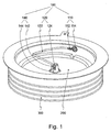
- Fig. 1 shows a view into the interior of a power semiconductor module according to the invention, here a disk cell. Shown is a ceramic housing (300), herein arranged a power semiconductor device (200) here specifically a power thyristor.
- the power thyristor (200) has a central location Auxiliary connection contact, here the control connection contact.
- the remaining area serves as a load, in this case as a cathode contact. Its load connection to the outside is not shown here, however, corresponds essentially to the prior art, thus has a recess for the arrangement of the auxiliary terminal (100).
- the auxiliary terminal (100) itself is formed from a contact device (140), an electrically conductive connecting element (120) and a contact element (110), which is formed partly as a clamping disk (114).
- the connecting element is designed as a contact pin (124) with a subsequent wire element (122).
- the contact pin is held and guided by means of the contact device (140).
- This contact device (140) consists of a plastic molded body (144) and a spring element (142).
- the contact pin (124) is designed in such a way that pressure is exerted on the contact device (120) after the disc cell has been mounted, pressing the contact pin (130) onto the auxiliary terminal contact of the power semiconductor component (200) and thus safely and permanently connecting the auxiliary terminal (100) electrically contacted.
- the second end of the auxiliary terminal (100) forms the contact element (110).
- This is formed as a metal molding with a crimp (112).
- the wire element (120) is electrically connected by means of a crimp connection.
- the contact element (110) further comprises a clamping disc (114) which is arranged on a pin-like metal molded part of an outer connection element.
- Fig. 2 shows a section through the middle of the disc cell Fig. 1 , Shown is also the cylindrical housing (300) whose outer surface is wavy for reasons of electrical safety.
- the housing (300) has an outer connection element (310).
- This connection element is formed in the interior of the housing (300) as a pin-like metal molding.
- the Hautpan gleichInstitutelement (190) of the anode is here designed as a metallic cylinder, on which a further metallic disc, preferably made of molybdenum, and thereon the power semiconductor component (200) is arranged.
- the auxiliary terminal (100) for connecting the auxiliary terminal contact of the power semiconductor component (200) to the outer terminal element (310) is in turn formed from the contact device (140), the electrically conductive connecting element (120) and the contact element (110).
- the arrangement of the contact element (110) on the pin-like metal mold part of the outer connection element (310) is also shown here.
- auxiliary connection (100) protrudes only very slightly into the interior space of the pane cell in the region of the outer connection element (310) and thus leaves sufficient space for the load connection element, not shown, of the cathode.
- the plastic molded body (142) of the contact device (140) is printed in the direction of the power semiconductor component (200).
- the spring element (144) pressure is exerted on the contact pin (124), which is thus electrically and permanently connected to the auxiliary terminal contact of the power semiconductor component (200).
- the auxiliary terminal (100) can also start from a substrate which is designed as an auxiliary board in the interior of the housing. This substrate then has at least one metallic surface, which is electrically conductively connected to the control terminal of the semiconductor component by means of a wire bond connection.
- Fig. 3 shows the contact element (110) according to the invention both in plan view and in three-dimensional representation.
- the contact element (110) is the connecting link of the auxiliary connection (100) with an outer connection element (310).
- the contact element (110) is formed as a metal molded part with a crimped connection (112) for crimping the connection element (120) designed as a wire element and with a clamping disk (112).
- the clamping disc consists of an outer ring (118) with preferably three, or not shown here, five isolated clamping lips (116).
- the diameter of the central recess of the clamping disk (114) is preferably smaller by 0.1 mm to 0.5 mm than the diameter of the pin-like metal molded part of the outer connecting element (310, cf. Fig. 1 ).
- the clamping lips (116) are pre-bent out of the plane formed by the outer ring (118) in the direction of the interior of the power semiconductor module.
- the tangent of the angle of the clamping lips to the plane is smaller than the sliding friction factor between the materials of the pin-like molded part of the outer connecting element (310) and the clamping disc (114).
- the angular range of the pre-bend is then between this critical angle and the half limit angle.
Landscapes
- Die Bonding (AREA)
- Connection Of Batteries Or Terminals (AREA)
- Connecting Device With Holders (AREA)
- Details Of Connecting Devices For Male And Female Coupling (AREA)
- Connector Housings Or Holding Contact Members (AREA)
Description
- Es wird ein Leistungshalbleitermodul vorgeschlagen mit einer sicheren internen Verbindung des Hilfsanschlusskontakts eines darin angeordneten Leistungshalbleiterbauelements mit einem äußeren Anschlusselement. Bekannt sind verschienen Ausgestaltungen von Leistungshalbleitermodulen, beispielhaft mit einem Substrat mit einer Mehrzahl hierauf angeordneter Leistungshalbleiterbauelemente und einem diese umhüllenden Kunststoffgehäuses. Zum Teil weisen derartige Leistungshalbleitermodule auch metallische Grundplatten auf. Ebenso bekannt sind Scheibenzellen mit einem hermetisch dichten Gehäuse und meist nur einem einzelnen Halbleiterbauelement in ihrem Inneren. Die vorgeschlagenen Ausgestaltungen sind für alle Arten von Leistungshalbleitermodulen geeignet, weisen aber speziell für Scheibenzellen besondere Vorteile auf.
- Die Erfindung wird daher auch am Beispiel einer Scheibenzelle beschreiben, wie sie seit langem bekannter Stand der Technik ist und vielfältig hergestellt wird. Derartige Scheibenzellen bestehen wie beispielhaft an der
DE 101 32 169 A1 ersichtlich aus einem zylinderförmigen lsolierstoffkörper als Gehäuse. Hierin angeordnet ist mindestens ein Leistungshalbleiterbauelement, beispielhaft eine Leistungsdiode, eine Leistungstransistor oder ein Leistungsthyristor. Die Erfindung betrifft hier hauptsächlich diejenigen Scheibenzellen mit gesteuerten Leistungshalbleiterbauelementen in ihrem Inneren. - Unter Hilfsanschluss wird daher hauptsächlich die Verbindung des Steueranschlusses des Leistungshalbleiterbauelements verstanden. Ebenso sind aber auch Hilfsemitteranschlüsse oder Anschlüsse für im Leistungshalbleitermodul integrierte Sensoren unter dem Begriff subsumiert.
- Die Hilfsanschlüsse einer Scheibenzelle sind nach dem Stand der Technik ausgestaltet als eine Kontakteinrichtung zur Verbindung des Hilfsanschlusses mit dem Hilfsanschlusskontakt des Leistungshalbleiterbauelements, einem Verbindungselement und einem Kontaktelement zur Verbindung mit einem äußeren Anschlusselement, in der Regel einer Durchkontaktierung des Gehäuses.
- Die Kontakteinrichtung zur Verbindung des Hilfsanschlusses mit dem Hilfsanschlusskontakt des Leistungshalbleiterbauelements ist entweder als stoffschlüssige Verbindung, meist als Lötverbindung, oder als stoffbündige Verbindung, meist als Druckkontaktierung, ausgestaltet. Lötverbindung sind in der Regel nachteilig, das sie im Vergleich mit anderen Verbindungstechniken die geringste Dauerhaltbarkeit aufweisen. Druckkontaktierte Verbindungen sind in eine Vielzahl von Varianten bekannt, wobei eine neuere Variante in der nicht vorveröffentlichten
DE 10 2004 050 588 offenbart wird. - Ausgehend von dieser Kontakteinrichtung besteht der Hilfsanschluss meist aus einem elektrisch isolierten Drahtelement, das an dem Anschlusselement angelötet oder angeschweißt ist. Hierbei hat die Schweißverbindung den Vorteil der größeren Dauerhaltbarkeit. Alle bekannten stoffbündigen Lösungen weisen den Nachteil auf, dass durch deren Herstellung das Innere der Scheibenzelle, speziell einer der eng benachbarten Lastanschlusskontakte verschmutz wird und somit die Dauerhaltbarkeit beeinträchtigt wird. Lötverbindung weisen zudem den Nachteil auf, dass durch die Herstellung einer Lötverbindung beim externen Anschluss die interne Lötverbindung gelöst wird.
- Für Leistungshalbeitermodule mit einem Substrat ist es ebenfalls notwendig, dass die Hilfsanschlüsse, ausgehend von den Leistungshalbleitbauelementen oder von Leiterbahnen des Substrats als sichere und dauerhaltbare elektrische Verbindungen ausgestaltet sind.
- Aus der
FR 2 079 196 - Aus der
EP 0421 344 A1 ist ein Halbleitermodul, das ein halbleitendes Substrat aufweist, bekannt. - Aus der
EP 1 225 634 A2 ist ein Halbleitermodul, das mehrere halbleitende Elemente aufweist, bekannt. - Aus der
GB 918 543 - Aus der
DE 44 43 611 A1 ist ein Gate-Anschlußsystem für einen unter Druck zusammengebauten Hochleistungs-Thyristor mit Gate-Mittelelektrode bekannt. - Der Erfindung liegt die Aufgabe zugrunde ein Leistungshalbleitermodul, vorzugsweise eine Scheibenzelle, vorzustellen, mit einem äußeren Anschlusselement für Hilfsanschlüsse eines Leistungshalbleiterbauelements und / oder eines Substrats welches eine sichere und dauerhaltbare elektrische Verbindung erlaubt und welches einer einfachen Montage zugänglich ist.
- Die Aufgabe wird erfindungsgemäß gelöst, durch die Maßnahmen der Merkmale des Anspruchs 1. Bevorzugte Ausführungsformen sind in den Unteransprüchen beschrieben.
- Das erfindungsgemäße Leistungshalbleitermodul weist ein Gehäuse, mindestens ein im Inneren des Gehäuses angeordnetes Leistungshalbleiterbauelement sowie mindestens zwei Last- und mindestens einen Hilfsanschluss auf. Besonders bevorzugt ist, bei einem als Scheibenzelle ausgebildet Leistungshalbleitermodul, dass dessen Gehäuse mit dem äußeren Anschlusselementen hermetisch dicht ausgebildet ist.
- Das Leistungshalbleitermodul weist weiterhin mindestens einen Hilfsanschluss von dem Leistungshalbleiterbauelement, vorzugsweise von dessen Steueranschlusskontakt, ausgehend auf. Alternativ kann dieser Hilfsanschluss auch von einem Substrat ausgehen. Der jeweilige Hilfsanschluss endet an einem zugeordneten äußeren Anschusselement, wobei das jeweilige äußere Anschlusselement das Gehäuse durchdringt. Im Inneren des Gehäuses ist dieses Anschlusselement hierbei als stiftartiges Metallformteil ausgebildet.
- Der Hilfsanschluss selbst wird gebildet durch eine Kontakteinrichtung am Hilfsanschlusskontakt des Leistungshalbleiterbauelements bzw. einem entsprechenden Anschlusskontakt des Substrats, weiterführend mittels eines elektrisch leitenden Verbindungselements und endend in ein zum Teil als Klemmscheibe ausgebildeten Kontaktelement. Hierbei ist die Klemmscheibe auf dem stiftartigen Metallformteil des äußeren Anschlusselements angeordnet.
- Das Kontaktelement ist ausgebildet als ein Metallformteil mit einem Crimpanschluss zur Quetschverbindung mit dem als elektrisch isoliertes Drahtelement ausgestalteten Verbindungselement. Die Klemmscheibe ist ausgebildet als ein äußerer Ring mit einer Mehrzahl, vorzugsweise drei oder fünf, freigestellter Klemmlippen.
- Bevorzugt ist die Kontakteinrichtung am Hilfsanschlusskontakt des Leistungshalbleiterbauelements ausgebildet als ein Kunststoffformteil zur Fixierung eines Kontaktzapfens und als ein Federelement zur druckkontaktierten Verbindung des Kontaktzapfens mit dem Hilfsanschlusskontakt des Leistungshalbleiterbauelements..
- Der erfinderische Gedanke wird anhand des Ausführungsbeispiels der
Fig. 1 bis 3 näher erläutert. -
Fig. 1 zeigt eine dreidimensionale Darstellung einer Scheibenzelle. -
Fig. 2 zeigt einen Schnitt durch die Mitte dieser Scheibenzelle. -
Fig. 3 zeigt das erfindungsgemäße Kontaktelement zur Verbindung des Hilfsanschlusses mit einem äußeren Anschlusselement. -
Fig. 1 zeigt einen Blick ins Innere eines erfindungsgemäßen Leistungshalbleitermoduls, hier einer Scheibenzelle. Dargestellt ist ein Keramikgehäuse (300), hierin angeordnet ein Leistungshalbleiterbauelement (200) hier speziell ein Leistungsthyristor. Der Leistungsthyristor (200) weist einen zentral gelegenen Hilfsanschlusskontakt, hier den Steueranschlusskontakt, auf. Die restliche Fläche dient als Last-, hier als Kathodenkontakt. Dessen Lastanschluss nach außen ist hier nicht gezeigt, entspricht allerdings im Wesentlichen dem Stand der Technik, weist also eine Ausnehmung zur Anordnung des Hilfsanschlusses (100) auf. - Der Hilfsanschluss (100) selbst wird gebildet aus einer Kontakteinrichtung (140), einem elektrisch leitenden Verbindungselement (120) und einem zum Teil als Klemmscheibe (114) ausgebildeten Kontaktelement (110). Hierbei ist das Verbindungselement ausgebildet als ein Kontaktzapfen (124) mit einem anschließenden Drahtelement (122). Der Kontaktzapfen ist mittels der Kontakteinrichtung (140) gehaltert und geführt. Diese Kontakteinrichtung (140) besteht aus einem Kunststoffformkörper (144) und einem Federelement (142). Der Kontaktzapfen (124) ist derart ausgebildet, dass nach der Montage der Scheibenzelle Druck auf die Kontakteinrichtung (120) ausgeübt wird, diese den Kontaktzapfen (130) auf den Hilfsanschlusskontakt des Leistungshalbleiterbauelements (200) drückt und somit den Hilfsanschluss (100) sicher und dauerhaft elektrisch kontaktiert.
- Das zweite Ende des Hilfsanschlusses (100) bildet das Kontaktelement (110). Dieses ist ausgebildet als ein Metallformteil mit einem Crimpanschluss (112). Hiermit ist das Drahtelement (120) mittels einer Quetschverbindung elektrisch verbunden. Das Kontaktelement (110) weist weiterhin eine Klemmscheibe (114) auf, die auf einem stiftartigen Metallformteil eines äußeren Anschlusselements angeordnet ist.
-
Fig. 2 zeigt einen Schnitt durch die Mitte der Scheibenzelle nachFig. 1 . Dargestellt ist ebenfalls das zylinderförmige Gehäuse (300), dessen äußere Oberfläche aus Gründen der elektrischen Sicherheit wellenförmig ausgebildet ist. Das Gehäuse (300) weist ein äußeres Anschlusselement (310) auf. Dieses Anschlusselement ist im Inneren des Gehäuses (300) als stiftartiges Metallformteil ausgebildet. Das Hautpanschlusselement (190) der Anode ist hier als metallischer Zylinder ausgebildet, auf dem eine weitere metallische Scheibe, vorzugsweise aus Molybdän, und hierauf das Leistungshalbleiterbauelement (200) angeordnet ist. - Der Hilfsanschluss (100) zur Verbindung des Hilfsanschlusskontakts des Leistungshalbleiterbauelements (200) mit dem äußeren Anschlusselement (310) wird wiederum gebildet aus der Kontakteinrichtung (140), dem elektrisch leitenden Verbindungselement (120) und dem Kontaktelement (110). Die Anordnung des Kontaktelements (110) auf dem stiftartigen Metallformteil des äußeren Anschlusselements (310) ist hier ebenfalls dargestellt.
- Durch diese erfindungsgemäße Ausgestaltung des Hilfsanschlusses (100) ragt dieser im Bereich des äußeren Anschlusselements (310) nur sehr gering in den Innerraum der Scheibenzelle hinein und lässt somit ausreichend Platz für das nicht dargestellte Lastanschlusselement der Kathode. Mittels dieses Lastanschlusselements wird der Kunststoffformkörper (142) der Kontakteinrichtung (140) in Richtung des Leistungshalbleiterbauelements (200) gedruckt. Hierdurch wird mittels des Federelements (144) Druck auf den Kontaktzapfen (124) ausgeübt, der somit elektrisch sicher und dauerhaft mit dem Hilfsanschlusskontakt des Leistungshalbleiterbauelements (200) verbunden ist.
- Der Hilfsanschluss (100) kann alternativ zur oben genannten Ausgestaltung auch ausgehen von einem Substrat, das als eine Hilfsplatine im Inneren des Gehäuses ausgestaltet ist. Dieses Substrat weist dann mindestens eine metallische Oberfläche auf, die mit dem Steueranschluss des Halbleiterbauelements mittels einer Drahtbondverbindung elektrisch leitend verbunden ist.
-
Fig. 3 zeigt das erfindungsgemäße Kontaktelement (110) sowohl in Draufsicht als auch in dreidimensionaler Darstellung. Das Kontaktelement (110) ist das Verbindungsglied des Hilfsanschlusses (100) mit einem äußeren Anschlusselement (310). Das Kontaktelement (110) ist ausgebildet als ein Metallformteil mit einem Crimpanschluss (112) zur Quetschverbindung mit dem als Drahtelement ausgestalteten Verbindungselement (120) und mit einer Klemmscheibe (112). Die Klemmscheibe besteht aus einem äußeren Ring (118) mit vorzugsweise drei, oder hier nicht dargestellten fünf, freigestellten Klemmlippen (116). Der Durchmesser der zentralen Ausnehmung der Klemmscheibe (114) ist vorzugsweise um 0,1mm bis 0,5mm geringer als der Durchmesser des stiftartigen Metallformteils des äußeren Anschlusselements (310, vgl.Fig. 1 ). - Es ist besonders bevorzugt, wenn die Klemmlippen (116) aus der durch den äußeren Ring (118) gebildeten Ebene heraus in Richtung des Inneren des Leistungshalbleitermoduls vorgebogen sind. Hierbei hat es sich wiederum als besonders vorteilhaft erwiesen, wenn der Tangens des Winkels der Klemmlippen zur Ebene kleiner ist als der Gleitreibungsfaktor zwischen den Werkstoffen des stiftartigen Formteils des äußeren Anschlusselements (310) und der Klemmscheibe (114). Der Winkelbereich der Vorbiegung liegt dann zwischen diesem Grenzwinkel und dem Halben Grenzwinkel. Dadurch ist die Montage auf dem stiftartigen Metallformteil des äußeren Anschlusselements (310) vereinfacht und ein Herabrutschen sicher verhindert.
Claims (4)
- Leistungshalbleitermodul mit einem Gehäuse (300), mindestens einem im Inneren des Gehäuses (300) angeordneten Leistungshalbleiterbauelement (200), mindestens zwei Last- (190) und mindestens einem Hilfsanschluss (100), wobei der mindestens eine Hilfsanschluss (100) von dem Leistungshalbleiterbauelement (200) und / oder einem Substrat ausgeht und an einem zugeordneten äußeren Anschusselement (310) endet, wobei das mindestens eine äußere Anschlusselement (310) des mindestens einen Hilfsanschlusses (100) das Gehäuse (300) durchdringt und im Inneren als stiftartiges Metallformteil ausgebildet ist und wobei der Hilfsanschluss (100) gebildet wird durch eine Kontakteinrichtung (140) am Hilfsanschlusskontakt des Leistungshalbleiterbauelements (200) oder des Substrats, ein elektrisch leitendes Verbindungselement (120) und ein zum Teil als Klemmscheibe (114) ausgebildetes Kontaktelement (110), wobei die Klemmscheibe (114) auf dem stiftartigen Metallformteil des äußeren Anschlusselements (310) angeordnet ist, gekennzeichnet dadurch dass das Kontaktelement (110) ausgebildet ist als ein Metallformteil mit einem Crimpanschluss (112) zur Quetschverbindung mit dem als Drahtelement (122) ausgestalteten Verbindungselement (120) und der Klemmscheibe (112), die ausgestaltet ist als ein äußerer Ring (118) mit einer Mehrzahl freigestellter Klemmlippen (116).
- Leistungshalbleitermodul nach Anspruch 1,
wobei die Klemmlippen (116) aus der durch den äußeren Ring (118) gebildeten Ebene heraus in Richtung des Inneren des Leistungshalbleitermoduls vorgebogen sind. - Leistungshalbleitermodul nach Anspruch 1,
wobei die Kontakteinrichtung (140) am Hilfsanschlusskontakt des Leistungshalbleiterbauelements (200) ein Kunststoffformteil zur Fixierung eines Kontaktzapfens (124) und ein Federelement zu druckkontaktierten Verbindung des Kontaktzapfens (124) mit dem Hilfsanschlusskontakt des Leistungshalbleiterbauelements (200) aufweist. - Leistungshalbleitermodul nach Anspruch 1,
wobei das Leistungshalbleitermodul als Scheibenzelle ausgebildet ist, deren Gehäuse (300) mit dem äußeren Anschlusselement (310) hermetisch dicht ausgebildet ist und wobei das Substrat als eine Hilfsplatine im Inneren des Gehäuse ausgestaltet ist.
Applications Claiming Priority (1)
| Application Number | Priority Date | Filing Date | Title |
|---|---|---|---|
| DE102004058946A DE102004058946B4 (de) | 2004-12-08 | 2004-12-08 | Leistungshalbleitermodul mit Hilfsanschluss |
Publications (3)
| Publication Number | Publication Date |
|---|---|
| EP1670056A2 EP1670056A2 (de) | 2006-06-14 |
| EP1670056A3 EP1670056A3 (de) | 2009-03-11 |
| EP1670056B1 true EP1670056B1 (de) | 2014-06-11 |
Family
ID=35888864
Family Applications (1)
| Application Number | Title | Priority Date | Filing Date |
|---|---|---|---|
| EP05025505.8A Expired - Lifetime EP1670056B1 (de) | 2004-12-08 | 2005-11-23 | Leistungshalbleitermodul mit Hilfsanschluss |
Country Status (6)
| Country | Link |
|---|---|
| US (1) | US7288842B2 (de) |
| EP (1) | EP1670056B1 (de) |
| JP (1) | JP4677328B2 (de) |
| KR (1) | KR101111038B1 (de) |
| CN (1) | CN100565858C (de) |
| DE (1) | DE102004058946B4 (de) |
Families Citing this family (2)
| Publication number | Priority date | Publication date | Assignee | Title |
|---|---|---|---|---|
| DE102006034964B3 (de) * | 2006-07-28 | 2007-09-06 | Semikron Elektronik Gmbh & Co. Kg | Anordnung mit einem Leistungshalbleiterbauelement und mit einer Kontakteinrichtung |
| DE102011076324B4 (de) * | 2011-05-24 | 2014-04-10 | Semikron Elektronik Gmbh & Co. Kg | Leistungselektronisches System mit Verbindungseinrichtung erster und zweiter Subsysteme |
Citations (1)
| Publication number | Priority date | Publication date | Assignee | Title |
|---|---|---|---|---|
| DE2104726A1 (de) * | 1970-02-02 | 1972-08-10 | Gen Electric | Halbleiterbauelement |
Family Cites Families (14)
| Publication number | Priority date | Publication date | Assignee | Title |
|---|---|---|---|---|
| DE6610823U (de) * | 1976-12-09 | Semikron Gesellschaft Fuer Gleichrichterbau Und Elektronik Mbh, 8500 Nuernberg | Halbleiteranordnung | |
| GB915676A (en) * | 1958-11-04 | 1963-01-16 | Ass Elect Ind | Improvements relating to electric rectifiers embodying semi-conductor material |
| US3448352A (en) * | 1966-07-26 | 1969-06-03 | Westinghouse Electric Corp | Multiple electrical contact assembly for compression bonded electrical devices |
| US3457988A (en) * | 1967-05-15 | 1969-07-29 | Westinghouse Electric Corp | Integral heat sink for semiconductor devices |
| US3513361A (en) * | 1968-05-09 | 1970-05-19 | Westinghouse Electric Corp | Flat package electrical device |
| CS214034B1 (en) * | 1980-06-10 | 1982-04-09 | Michal Pellant | Semiconductor modulus |
| DE3604313A1 (de) * | 1986-02-12 | 1987-08-13 | Bbc Brown Boveri & Cie | Leistungshalbleitermodul |
| JPH0680818B2 (ja) * | 1989-10-02 | 1994-10-12 | 株式会社東芝 | 電力用圧接型半導体装置 |
| US5436473A (en) * | 1993-12-30 | 1995-07-25 | International Rectifier Corporation | Gate lead for center gate pressure assembled thyristor |
| JP3588503B2 (ja) * | 1995-06-20 | 2004-11-10 | 株式会社東芝 | 圧接型半導体装置 |
| JP2001291536A (ja) * | 2000-04-10 | 2001-10-19 | Nec Corp | 導電布と電線との接続端子 |
| JP3954314B2 (ja) * | 2001-01-23 | 2007-08-08 | 株式会社東芝 | 圧接型半導体装置 |
| DE10132169B4 (de) * | 2001-07-03 | 2006-04-27 | eupec Europäische Gesellschaft für Leistungshalbleiter mbH & Co. KG | Halbleitermodul |
| DE102004050588B4 (de) * | 2004-10-16 | 2009-05-20 | Semikron Elektronik Gmbh & Co. Kg | Anordnung mit einem Leistungshalbleiterbauelement und mit einer Kontakteinrichtung |
-
2004
- 2004-12-08 DE DE102004058946A patent/DE102004058946B4/de not_active Expired - Lifetime
-
2005
- 2005-11-14 JP JP2005328643A patent/JP4677328B2/ja not_active Expired - Fee Related
- 2005-11-23 EP EP05025505.8A patent/EP1670056B1/de not_active Expired - Lifetime
- 2005-12-06 KR KR1020050117913A patent/KR101111038B1/ko not_active Expired - Fee Related
- 2005-12-07 CN CNB2005101310646A patent/CN100565858C/zh not_active Expired - Fee Related
- 2005-12-08 US US11/297,690 patent/US7288842B2/en not_active Expired - Lifetime
Patent Citations (1)
| Publication number | Priority date | Publication date | Assignee | Title |
|---|---|---|---|---|
| DE2104726A1 (de) * | 1970-02-02 | 1972-08-10 | Gen Electric | Halbleiterbauelement |
Also Published As
| Publication number | Publication date |
|---|---|
| EP1670056A3 (de) | 2009-03-11 |
| DE102004058946B4 (de) | 2009-06-18 |
| KR101111038B1 (ko) | 2012-02-17 |
| US7288842B2 (en) | 2007-10-30 |
| CN1787210A (zh) | 2006-06-14 |
| EP1670056A2 (de) | 2006-06-14 |
| JP2006165536A (ja) | 2006-06-22 |
| JP4677328B2 (ja) | 2011-04-27 |
| KR20060064532A (ko) | 2006-06-13 |
| DE102004058946A1 (de) | 2006-06-14 |
| US20060152952A1 (en) | 2006-07-13 |
| CN100565858C (zh) | 2009-12-02 |
Similar Documents
| Publication | Publication Date | Title |
|---|---|---|
| EP1145610B1 (de) | Elektronisches steuergerät | |
| EP2036410B1 (de) | Verfahren zur Fixierung einer Leiterplatte in einem Gehäuse und Anordnung mit einem Gehäuse, einer Leiterplatte und einem Fixierelement | |
| EP1004145B1 (de) | Optoelektronisches bauelement | |
| DE102009037257B4 (de) | Leistungshalbleitermodul mit Schaltungsträger und Lastanschlusselement sowie Herstellungsverfahren hierzu | |
| AT503687B1 (de) | Steuergerät mit einem stirnseitig kontaktierten schaltungsträger | |
| EP1830404A2 (de) | Leistungshalbleitermodul und zugehöriges Herstellungsverfahren | |
| WO2003034467A2 (de) | Leistungshalbleitermodul | |
| EP1843393A2 (de) | Leistungshalbleitermodul in Druckkontaktausführung | |
| EP2091080B1 (de) | Leistungshalbleitermodul mit einem Substrat und einer Druckeinrichtung | |
| EP0976165A1 (de) | Piezoaktor mit neuer kontaktierung und herstellverfahren | |
| EP1648029B1 (de) | Kontakteinrichtung für Leistungshalbleitermodule und Halbleiter-Scheibenzellen | |
| EP1933379A2 (de) | Leistungshalbleitermodul mit Kontaktfedern | |
| EP2194769B1 (de) | Leistungshalbleitermodul mit vorgespannter Hilfskontaktfeder | |
| EP1119823A1 (de) | Biometrischer sensor und verfahren zu dessen herstellung | |
| EP1883108B1 (de) | Anordnung mit einem Leistungshalbleiterbauelement und einer Kontakteinrichtung | |
| EP1933380A2 (de) | Leistungshalbleitermodul mit Kontaktfedern | |
| EP3979313B1 (de) | Leistungselektronische einrichtung und leistungshalbleitermodul damit | |
| DE19523977A1 (de) | Microchip-Sicherung | |
| EP2456970A1 (de) | Piezoaktor mit elektrischer kontaktierung | |
| EP1670056B1 (de) | Leistungshalbleitermodul mit Hilfsanschluss | |
| WO2008017556A2 (de) | Moldgehäuse in einpresstechnik | |
| EP1791178B1 (de) | Leistungshalbleitermodul in Druckkontaktausführung | |
| EP2447991A2 (de) | Kontaktelement und Verwendung eines Kontaktelements in einem elektronischen Bauteil | |
| WO2004068921A2 (de) | Elektronisches bauelement | |
| DE102012105995B4 (de) | Oberflächenmontierbare elektrische Einrichtung |
Legal Events
| Date | Code | Title | Description |
|---|---|---|---|
| PUAI | Public reference made under article 153(3) epc to a published international application that has entered the european phase |
Free format text: ORIGINAL CODE: 0009012 |
|
| AK | Designated contracting states |
Kind code of ref document: A2 Designated state(s): AT BE BG CH CY CZ DE DK EE ES FI FR GB GR HU IE IS IT LI LT LU LV MC NL PL PT RO SE SI SK TR |
|
| AX | Request for extension of the european patent |
Extension state: AL BA HR MK YU |
|
| PUAL | Search report despatched |
Free format text: ORIGINAL CODE: 0009013 |
|
| AK | Designated contracting states |
Kind code of ref document: A3 Designated state(s): AT BE BG CH CY CZ DE DK EE ES FI FR GB GR HU IE IS IT LI LT LU LV MC NL PL PT RO SE SI SK TR |
|
| AX | Request for extension of the european patent |
Extension state: AL BA HR MK YU |
|
| 17P | Request for examination filed |
Effective date: 20090309 |
|
| 17Q | First examination report despatched |
Effective date: 20090421 |
|
| AKX | Designation fees paid |
Designated state(s): AT BE BG CH CY CZ DE DK EE ES FI FR GB GR HU IE IS IT LI LT LU LV MC NL PL PT RO SE SI SK TR |
|
| GRAP | Despatch of communication of intention to grant a patent |
Free format text: ORIGINAL CODE: EPIDOSNIGR1 |
|
| INTG | Intention to grant announced |
Effective date: 20140310 |
|
| GRAS | Grant fee paid |
Free format text: ORIGINAL CODE: EPIDOSNIGR3 |
|
| GRAA | (expected) grant |
Free format text: ORIGINAL CODE: 0009210 |
|
| AK | Designated contracting states |
Kind code of ref document: B1 Designated state(s): AT BE BG CH CY CZ DE DK EE ES FI FR GB GR HU IE IS IT LI LT LU LV MC NL PL PT RO SE SI SK TR |
|
| REG | Reference to a national code |
Ref country code: GB Ref legal event code: FG4D Free format text: NOT ENGLISH |
|
| REG | Reference to a national code |
Ref country code: CH Ref legal event code: EP |
|
| REG | Reference to a national code |
Ref country code: IE Ref legal event code: FG4D Free format text: LANGUAGE OF EP DOCUMENT: GERMAN |
|
| REG | Reference to a national code |
Ref country code: AT Ref legal event code: REF Ref document number: 672610 Country of ref document: AT Kind code of ref document: T Effective date: 20140715 |
|
| REG | Reference to a national code |
Ref country code: DE Ref legal event code: R096 Ref document number: 502005014391 Country of ref document: DE Effective date: 20140717 |
|
| PG25 | Lapsed in a contracting state [announced via postgrant information from national office to epo] |
Ref country code: LT Free format text: LAPSE BECAUSE OF FAILURE TO SUBMIT A TRANSLATION OF THE DESCRIPTION OR TO PAY THE FEE WITHIN THE PRESCRIBED TIME-LIMIT Effective date: 20140611 Ref country code: GR Free format text: LAPSE BECAUSE OF FAILURE TO SUBMIT A TRANSLATION OF THE DESCRIPTION OR TO PAY THE FEE WITHIN THE PRESCRIBED TIME-LIMIT Effective date: 20140912 Ref country code: FI Free format text: LAPSE BECAUSE OF FAILURE TO SUBMIT A TRANSLATION OF THE DESCRIPTION OR TO PAY THE FEE WITHIN THE PRESCRIBED TIME-LIMIT Effective date: 20140611 |
|
| REG | Reference to a national code |
Ref country code: NL Ref legal event code: VDEP Effective date: 20140611 |
|
| REG | Reference to a national code |
Ref country code: LT Ref legal event code: MG4D |
|
| PG25 | Lapsed in a contracting state [announced via postgrant information from national office to epo] |
Ref country code: SE Free format text: LAPSE BECAUSE OF FAILURE TO SUBMIT A TRANSLATION OF THE DESCRIPTION OR TO PAY THE FEE WITHIN THE PRESCRIBED TIME-LIMIT Effective date: 20140611 Ref country code: LV Free format text: LAPSE BECAUSE OF FAILURE TO SUBMIT A TRANSLATION OF THE DESCRIPTION OR TO PAY THE FEE WITHIN THE PRESCRIBED TIME-LIMIT Effective date: 20140611 |
|
| PG25 | Lapsed in a contracting state [announced via postgrant information from national office to epo] |
Ref country code: EE Free format text: LAPSE BECAUSE OF FAILURE TO SUBMIT A TRANSLATION OF THE DESCRIPTION OR TO PAY THE FEE WITHIN THE PRESCRIBED TIME-LIMIT Effective date: 20140611 Ref country code: ES Free format text: LAPSE BECAUSE OF FAILURE TO SUBMIT A TRANSLATION OF THE DESCRIPTION OR TO PAY THE FEE WITHIN THE PRESCRIBED TIME-LIMIT Effective date: 20140611 Ref country code: SK Free format text: LAPSE BECAUSE OF FAILURE TO SUBMIT A TRANSLATION OF THE DESCRIPTION OR TO PAY THE FEE WITHIN THE PRESCRIBED TIME-LIMIT Effective date: 20140611 Ref country code: CZ Free format text: LAPSE BECAUSE OF FAILURE TO SUBMIT A TRANSLATION OF THE DESCRIPTION OR TO PAY THE FEE WITHIN THE PRESCRIBED TIME-LIMIT Effective date: 20140611 Ref country code: RO Free format text: LAPSE BECAUSE OF FAILURE TO SUBMIT A TRANSLATION OF THE DESCRIPTION OR TO PAY THE FEE WITHIN THE PRESCRIBED TIME-LIMIT Effective date: 20140611 |
|
| PG25 | Lapsed in a contracting state [announced via postgrant information from national office to epo] |
Ref country code: IS Free format text: LAPSE BECAUSE OF FAILURE TO SUBMIT A TRANSLATION OF THE DESCRIPTION OR TO PAY THE FEE WITHIN THE PRESCRIBED TIME-LIMIT Effective date: 20141011 Ref country code: NL Free format text: LAPSE BECAUSE OF FAILURE TO SUBMIT A TRANSLATION OF THE DESCRIPTION OR TO PAY THE FEE WITHIN THE PRESCRIBED TIME-LIMIT Effective date: 20140611 Ref country code: PL Free format text: LAPSE BECAUSE OF FAILURE TO SUBMIT A TRANSLATION OF THE DESCRIPTION OR TO PAY THE FEE WITHIN THE PRESCRIBED TIME-LIMIT Effective date: 20140611 |
|
| REG | Reference to a national code |
Ref country code: DE Ref legal event code: R097 Ref document number: 502005014391 Country of ref document: DE |
|
| PLBE | No opposition filed within time limit |
Free format text: ORIGINAL CODE: 0009261 |
|
| STAA | Information on the status of an ep patent application or granted ep patent |
Free format text: STATUS: NO OPPOSITION FILED WITHIN TIME LIMIT |
|
| PG25 | Lapsed in a contracting state [announced via postgrant information from national office to epo] |
Ref country code: DK Free format text: LAPSE BECAUSE OF FAILURE TO SUBMIT A TRANSLATION OF THE DESCRIPTION OR TO PAY THE FEE WITHIN THE PRESCRIBED TIME-LIMIT Effective date: 20140611 Ref country code: IT Free format text: LAPSE BECAUSE OF FAILURE TO SUBMIT A TRANSLATION OF THE DESCRIPTION OR TO PAY THE FEE WITHIN THE PRESCRIBED TIME-LIMIT Effective date: 20140611 |
|
| 26N | No opposition filed |
Effective date: 20150312 |
|
| REG | Reference to a national code |
Ref country code: DE Ref legal event code: R097 Ref document number: 502005014391 Country of ref document: DE Effective date: 20150312 |
|
| PG25 | Lapsed in a contracting state [announced via postgrant information from national office to epo] |
Ref country code: MC Free format text: LAPSE BECAUSE OF FAILURE TO SUBMIT A TRANSLATION OF THE DESCRIPTION OR TO PAY THE FEE WITHIN THE PRESCRIBED TIME-LIMIT Effective date: 20140611 Ref country code: LU Free format text: LAPSE BECAUSE OF FAILURE TO SUBMIT A TRANSLATION OF THE DESCRIPTION OR TO PAY THE FEE WITHIN THE PRESCRIBED TIME-LIMIT Effective date: 20141123 Ref country code: BE Free format text: LAPSE BECAUSE OF NON-PAYMENT OF DUE FEES Effective date: 20141130 |
|
| REG | Reference to a national code |
Ref country code: CH Ref legal event code: PL |
|
| GBPC | Gb: european patent ceased through non-payment of renewal fee |
Effective date: 20141123 |
|
| PG25 | Lapsed in a contracting state [announced via postgrant information from national office to epo] |
Ref country code: LI Free format text: LAPSE BECAUSE OF NON-PAYMENT OF DUE FEES Effective date: 20141130 Ref country code: CH Free format text: LAPSE BECAUSE OF NON-PAYMENT OF DUE FEES Effective date: 20141130 Ref country code: SI Free format text: LAPSE BECAUSE OF FAILURE TO SUBMIT A TRANSLATION OF THE DESCRIPTION OR TO PAY THE FEE WITHIN THE PRESCRIBED TIME-LIMIT Effective date: 20140611 |
|
| REG | Reference to a national code |
Ref country code: IE Ref legal event code: MM4A |
|
| REG | Reference to a national code |
Ref country code: FR Ref legal event code: ST Effective date: 20150731 |
|
| PG25 | Lapsed in a contracting state [announced via postgrant information from national office to epo] |
Ref country code: IE Free format text: LAPSE BECAUSE OF NON-PAYMENT OF DUE FEES Effective date: 20141123 Ref country code: GB Free format text: LAPSE BECAUSE OF NON-PAYMENT OF DUE FEES Effective date: 20141123 |
|
| PG25 | Lapsed in a contracting state [announced via postgrant information from national office to epo] |
Ref country code: FR Free format text: LAPSE BECAUSE OF NON-PAYMENT OF DUE FEES Effective date: 20141201 |
|
| REG | Reference to a national code |
Ref country code: AT Ref legal event code: MM01 Ref document number: 672610 Country of ref document: AT Kind code of ref document: T Effective date: 20141123 |
|
| PG25 | Lapsed in a contracting state [announced via postgrant information from national office to epo] |
Ref country code: AT Free format text: LAPSE BECAUSE OF NON-PAYMENT OF DUE FEES Effective date: 20141123 |
|
| PG25 | Lapsed in a contracting state [announced via postgrant information from national office to epo] |
Ref country code: BG Free format text: LAPSE BECAUSE OF FAILURE TO SUBMIT A TRANSLATION OF THE DESCRIPTION OR TO PAY THE FEE WITHIN THE PRESCRIBED TIME-LIMIT Effective date: 20140611 |
|
| PG25 | Lapsed in a contracting state [announced via postgrant information from national office to epo] |
Ref country code: PT Free format text: LAPSE BECAUSE OF FAILURE TO SUBMIT A TRANSLATION OF THE DESCRIPTION OR TO PAY THE FEE WITHIN THE PRESCRIBED TIME-LIMIT Effective date: 20140611 Ref country code: CY Free format text: LAPSE BECAUSE OF FAILURE TO SUBMIT A TRANSLATION OF THE DESCRIPTION OR TO PAY THE FEE WITHIN THE PRESCRIBED TIME-LIMIT Effective date: 20140611 |
|
| PG25 | Lapsed in a contracting state [announced via postgrant information from national office to epo] |
Ref country code: TR Free format text: LAPSE BECAUSE OF FAILURE TO SUBMIT A TRANSLATION OF THE DESCRIPTION OR TO PAY THE FEE WITHIN THE PRESCRIBED TIME-LIMIT Effective date: 20140611 Ref country code: HU Free format text: LAPSE BECAUSE OF FAILURE TO SUBMIT A TRANSLATION OF THE DESCRIPTION OR TO PAY THE FEE WITHIN THE PRESCRIBED TIME-LIMIT; INVALID AB INITIO Effective date: 20051123 |
|
| REG | Reference to a national code |
Ref country code: DE Ref legal event code: R084 Ref document number: 502005014391 Country of ref document: DE |
|
| PGFP | Annual fee paid to national office [announced via postgrant information from national office to epo] |
Ref country code: DE Payment date: 20241001 Year of fee payment: 20 |
|
| REG | Reference to a national code |
Ref country code: DE Ref legal event code: R081 Ref document number: 502005014391 Country of ref document: DE Owner name: SEMIKRON DANFOSS ELEKTRONIK GMBH & CO. KG, DE Free format text: FORMER OWNER: SEMIKRON ELEKTRONIK GMBH & CO. KG, 90431 NUERNBERG, DE |
|
| REG | Reference to a national code |
Ref country code: DE Ref legal event code: R071 Ref document number: 502005014391 Country of ref document: DE |