EP1670094B1 - Procédé de calibration d'un système d'antenne intelligente - Google Patents
Procédé de calibration d'un système d'antenne intelligente Download PDFInfo
- Publication number
- EP1670094B1 EP1670094B1 EP05026272.4A EP05026272A EP1670094B1 EP 1670094 B1 EP1670094 B1 EP 1670094B1 EP 05026272 A EP05026272 A EP 05026272A EP 1670094 B1 EP1670094 B1 EP 1670094B1
- Authority
- EP
- European Patent Office
- Prior art keywords
- calibration
- signal
- calibration signal
- data
- carriers
- Prior art date
- Legal status (The legal status is an assumption and is not a legal conclusion. Google has not performed a legal analysis and makes no representation as to the accuracy of the status listed.)
- Expired - Lifetime
Links
Images


Classifications
-
- H—ELECTRICITY
- H04—ELECTRIC COMMUNICATION TECHNIQUE
- H04B—TRANSMISSION
- H04B7/00—Radio transmission systems, i.e. using radiation field
- H04B7/02—Diversity systems; Multi-antenna system, i.e. transmission or reception using multiple antennas
-
- H—ELECTRICITY
- H01—ELECTRIC ELEMENTS
- H01Q—ANTENNAS, i.e. RADIO AERIALS
- H01Q3/00—Arrangements for changing or varying the orientation or the shape of the directional pattern of the waves radiated from an antenna or antenna system
- H01Q3/26—Arrangements for changing or varying the orientation or the shape of the directional pattern of the waves radiated from an antenna or antenna system varying the relative phase or relative amplitude of energisation between two or more active radiating elements; varying the distribution of energy across a radiating aperture
Definitions
- the present invention relates generally to a calibration apparatus and method for controlling the phase and amplitude of a signal in a smart antenna multicarrier communication system, and in particular, to an apparatus and method for transmitting a calibration signal on the remaining carriers after allocating data to carriers, thereby increasing the efficiency of frequency resource utilization for the data signal.
- a smart antenna system is a communication system that uses a plurality of antennas to automatically optimize a radiation pattern and/or a reception pattern according to a signal environment. From the perspective of data signal transmission, the smart antenna system transmits a signal with a desired strength in an intended direction at a minimum power level by beamforming.
- the use of the smart antenna enables a Base Station (BS) to direct a signal only to a desired Mobile Station (MS) through beamforming. Therefore, compared to omnidirectional signal transmission to all MSs, the smart antenna reduces power required for signal transmission and interference, as well. Since the smart antenna applies directionality to a transmission/received signal by actively locating an intended MS, interference to other MSs within the same cell can be minimized. Thus, the BS can allocate the remaining available power to other MSs and the reduced interference with other cells leads to the increase of BS channel capacity.
- a wireless internet service system based on Orthogonal Frequency Division Multiple Access uses a wide frequency bandwidth and transmits a signal from a BS to one MS at a higher power level than in a conventional system. Thus, a cell radius is small.
- Application of the smart antenna to the wireless internet system advantageously increases BS channel capacity.
- beamforming is performed by using a beamforming weight vector for each orthogonal frequency carrier of each antenna such that each antenna beam is steered in a chosen direction.
- the beams must reach the antennas without any change prior to transmission over the air, but they experience distortions in their phase and amplitude due to non-linear components in the BS.
- calibration is needed to control the phase and amplitude of the signals.
- the total performance of the smart antenna technology depends on the accuracy of the calibration, that is, the accuracy of beam directionality and minimization of phase mismatch.
- the calibration is commonly applied to a downlink directed from a BS to an MS and an uplink directed from an MS to a BS.
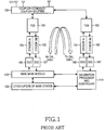
- FIG. 1 is a block diagram of a conventional calibration apparatus in a smart antenna system.
- a transmission (Tx) calibration signal is transferred in the following manner. First, a calibration signal generated from a calibration processor and controller 110 under the control of other layers of the BS 109 is provided to a baseband module 108. The calibration signal is then transmitted to antennas 101 through a Radio Frequency (RF) module.
- RF Radio Frequency
- the RF module oversamples the calibration signal in a Digital UpConverter (DUC) 106, modulates the oversampled signal to an RF signal in a Tx module 104, and transmits the modulated signal to the antennas 101 through a Transceiver Control Board (TCB) 103 and a coupler-splitter 102. Meanwhile, the calibration signal is coupled in the coupler-splitter 102 and transferred in a calibration path. Specifically, this calibration signal returns to the calibration processor and controller 110 through a TCB 103, a reception (Rx) module 105, and a Digital DownConverter (DDC) 107 in a Tx calibration path.
- DUC Digital UpConverter
- a calibration signal generated from the calibration processor and controller 110 passes through a DUC 106, a Tx module 104, and a TCB 103 in an Rx path and is coupled to signals received at the antennas 101 in a coupler-combiner 102.
- the coupled signal returns to the calibration processor and controller 110 through a TCB 103, an Rx module 105, a DDC 107, and the baseband module 109 in an Rx calibration path.
- calibration vectors are estimated for Tx calibration and Rx calibration by computing differences in phase and amplitude between calibration signals generated from the calibration processor and controller 110 and the calibration signals fed back from the Tx and Rx paths.
- FIG 2 illustrates the principle of calibration in the conventional smart antenna system.
- a Tx or Rx calibration signal C(t) experiences variations in its phase and amplitude as it travels in a path running to antennas and in a feedback path. Given N antennas, the calibration signal C(t) is received from N paths.
- C n (t) denotes a feedback calibration signal from an n th path
- ⁇ n denotes attenuation in the n th path.
- ⁇ N,cal is a phase factor for n th path
- ⁇ feedback is a phase factor for feedback path.
- a coupler characteristic R coupter from each path must be eliminated and for beamforming, the relative phases of the N antennas must be matched.
- Calibration vectors are computed by Equation 2.
- beamforming weight vectors for antennas are W b1 , W b2 , W bn
- beamforming weight vectors calculated taking antenna paths into account are W b1 W c1 , W b2 W c2 , W bn W cn .
- the calibration must be performed periodically for all carriers to use the smart antenna in a multicarrier communication system such as OFDMA.
- This calibration requires allocation of frequency resources to a calibration signal.
- the additional frequency resource allocation for the calibration signal leads to dissipation of frequency resources and thus there is a need for a technique of solving this problem.
- JP 2003 273634 A refers to an array antenna device in which a calibration is performed without stopping a receiving function in the array antenna device.
- a phase deviation arithmetic circuit carries out the calibration by introducing a calibration signal from a calibration signal generation circuit based upon selected synchronous switching operations to first and second switchers, when composing signals from respective antenna elements via phase shifters. Therefore, the other receiving system, except for a switched and selected receiving system, continues an ordinary receiving operation based upon a formed received beam pattern without being stagnated.
- US 6,208,287 B1 describes a phased array antenna calibration system and a respective method thereof.
- the described self-contained calibration and failure detection in a phase array antenna has a beam-forming network.
- the beam-forming network includes a plurality of array ports and a plurality of beam ports or a space fed system.
- a plurality of antenna elements and a plurality of transmit/receive modules are included. Each one of the modules is coupled between a corresponding one of the antenna elements and a corresponding one of the array ports.
- a calibration system is provided which has an RF input port, an RF detector port, an RF detector coupled to the RF detector port, and an antenna element port.
- a switch section is included for sequentially coupling each of the antenna elements through the beam-forming/space-fed network and the one of the transmit/receive modules coupled thereto selectively to either the detector port during a receive calibration mode or to the RF input port during a transmit calibration mode.
- the switch section includes a switch for selectively coupling a predetermined one of the antenna elements, i.e. a calibration antenna element, selectively to either the RF test input of the calibration system during the receive calibration mode through a path isolated from the beam-forming network or to the detector port during the transmit calibration mode through a path isolated from the beam-forming network.
- US 5,499,031 refers to a distributed receiver system for antenna array. It describes that in an antenna array of large dimensions, such as might be used for high frequency radar, the antennas will be connected by short feeders to receivers which will consequently be distributed over a considerable distance. Calibration of such an antenna array to compensate for variations in the transfer functions of the receivers will necessitate the same test signal being fed into each element in turn to measure the receiver output, and this could be time consuming and hence reduce the time available for use of the array.
- a loop is connected at various tappings to the feeders, the respective antennas are disconnected, and sinusoidal tones are injected into the left hand and right hand ends of the loop. The outputs of the receivers are measured, and provide a measure of the transfer functions of the receivers and hence enable discrepancies between them to be corrected.
- EP 1 416 655 refers to a calibration method in an OFDM system and injects calibration signals along the multiple subcarriers used in that OFDM system. Accordingly, an object of the present invention is to provide an improved calibration apparatus and method for controlling the phase and amplitude of a signal in a smart antenna multicarrier communication system.
- An aspect of the present invention is to provide a calibration apparatus and method for transmitting a calibration signal by which to control the phase and amplitude of a signal on the remaining carriers after allocating data to carriers, thereby increasing the efficiency of frequency resource utilization for the data signal in a smart antenna multicarrier communication system.
- the above aspect is achieved by providing a calibration apparatus and method for controlling the phase and amplitude of a signal in a smart antenna multicarrier communication system.
- a scheduler allocates a data signal to a plurality of carriers as data carriers, provides the data signal to a baseband processor, and controls a calibration processor and controller to generate a calibration signal to be allocated to non-data carriers to which the data signal is not allocated.
- the calibration processor and controller generates the calibration signal on the non-data carriers under the control of the scheduler and calculates a calibration vector using the calibration signal and a feedback calibration signal (the calibration signal passed through a transmission path).
- the baseband processor calibrates a beamforming weight vector for a data signal with the calibration vector and transmits the calibrated data signal in the transmission path.
- a data signal is allocated to a plurality of carriers as data carriers.
- a calibration signal is allocated to non-data carriers to which the data signal is not allocated and transmitted in a transmission path.
- a calibration vector is calculated using the calibration signal and a feedback calibration signal received from the transmission path.
- a beamforming weight vector is calibrated for the data signal using the calibration vector and the calibrated data signal is transmitted in the transmission path.
- a time threshold is predetermined so that, unless a specific carrier to which the calibration signal was allocated has the calibration signal applied again within that time threshold, the calibration signal is forcibly allocated to the carrier so that the calibration signal is allocated across the total frequency band periodically.
- Periodic calibration is needed for all carriers in application of a smart antenna to a multicarrier communication system like an Orthogonal Frequency Division Multiplexing (OFDM) or an Orthogonal Frequency Division Multiple Access (OFDMA) communication system.
- OFDM Orthogonal Frequency Division Multiplexing
- OFDMA Orthogonal Frequency Division Multiple Access
- FIG. 3 illustrates allocation of carriers to a data signal in a smart-antenna communication system according to the present invention.
- shaded squares denote areas with data signals and blank squares denote areas without data signals, somme of which are allocated to a calibration signal.
- An example of allocating carriers to data over time is shown herein. As different MSs are connected to a BS with passage of time, the allocation of frequency resources to data changes correspondingly, and carriers without data also change with passage of time, as well.
- FIG. 4 is a block diagram of a calibration apparatus in a smart antenna system according to the present invention.
- reference numerals 401 to 410 denote the same components 101 to 110 illustrated in FIG. 1 .
- Reference numerals 411 to 414 denote components further provided according to the present invention, for allocating a calibration signal to carriers and estimating calibration vectors.
- a scheduler 412 allocates a data signal to carriers taking into account calibration in each symbol and provides the data signal to a baseband processor 411.
- the scheduler 412 also controls a calibration signal generator 413 and a calibration vector processor 414.
- the scheduler 412 controls the calibration signal generator 413 to generate the calibration signal on non-data carriers and controls the calibration vector processor 414 to compute a calibration vector using a feedback calibration signal that has passed through a feedback path.
- This calibration signal is transmitted/received for Tx calibration and Rx calibration in the same manner as illustrated in FIG. 1 .
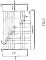
- FIG 5 illustrates the configuration of the baseband processor 411 in the smart antenna system according to the present invention.
- the baseband processor 411 in the baseband module 408 receives calibration vectors from the calibration vector processor 414 of the calibration processor and controller 410.
- a data mapper 504 maps non-data carriers to multipliers 502.
- a calibrator 503 provides the calibration vectors to multipliers 502.
- the multipliers 502 multiply the carrier signals with the calibration vectors and an inverse fast Fourier transform (IFFT)/FFT processor 501 modulates the products by IFFT.
- IFFT inverse fast Fourier transform
- the IFFT/FFT 501 demodulates a received data signal by FFT.
- the calibrator 503 applies the calibration vectors received from the calibration vector processor 414 to the FFT signals.
- FIG. 6 is a block diagram of the scheduler 412 in the smart antenna system according to the present invention.
- the scheduler 412 functions to allocate a calibration signal to carriers by controlling the calibration signal generator 413.
- a carrier-set finder 601 finds carriers whose timer values do not exceed a threshold (Time_threshold) as data carriers to which data can be allocated.
- a data allocater 603 allocates data to the carriers found by the carrier-set finder 601.
- a timer 602 updates its timer value for a corresponding data carrier to which the data allocater 603 has allocated data.
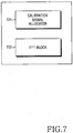
- FIG 7 is a block diagram of the calibration signal generator 413 in the smart antenna system according to the present invention.
- the calibration signal generator 413 includes a calibration signal allocater 701 and an IFFT processor 702.
- the calibration signal allocater 701 allocates a calibration signal to non-data carriers based on carrier-data allocation information received from the scheduler 412.
- the IFFT processor 702 modulates the calibration carrier signals by IFFT.
- FIG. 8 is a block diagram of the calibration vector processor 414 in the smart antenna system according to the present invention.
- the calibration vector processor 414 includes an FFT processor 801, a calibration signal acquirer 802, a calibration signal updater 803, an interpolator 804, and a calibration vector calculator 805.
- the FFT processor 801 separates a feedback calibration signal by carriers.
- the calibration signal acquirer 802 measures the phase and amplitude of the feedback calibration signals of calibration carriers according to calibration carrier position information received from the scheduler 412.
- the calibration signal updater 803 updates the phase and amplitude information each time and stores it in a memory.
- the interpolator 804 interpolates the stored phase and amplitude information, thereby estimating the phases and amplitudes of the calibration signal on carriers to which the calibration signal was not allocated. The interpolation is carried out in the case where a large number of MSs are connected to the BS.
- the calibration vector calculator 805 calculates calibration vectors after eliminating coupler characteristics from the feedback calibration signal.
- FIG. 9 is a flowchart illustrating an operation for allocating carriers to a calibration signal in the smart antenna system according to the present invention.
- a timer for each carrier is reset to 0 before the BS operates.
- a variable n indicating a carrier is set to 1 in step 901.
- the timer value of the n th carrier is compared with a timer threshold (Time_threshold). If timer value of the n th carrier is greater than the threshold, the n th carrier is excluded as unavailable as a data carrier in step 903. In this case n is updated to n+1 in step 904 and returned to step 902.
- the n th carrier may be data carriers in step 905. Because the data is not allocated to all data carriers, carriers for which the data is not allocated may exist. In step 906, it is confirmed whether data is allocated. If data is not allocated, then a calibration signal is allocated to such a non-data carrier in step 907. A symbol having the calibration signal and the data signal is then transmitted.
- FIG 10 is a flowchart illustrating an operation for estimating a calibration vector in the smart antenna system according to the present invention.
- a variable n indicating a carrier is set to 1 in step 1001. If n th is less than N(total number of carriers), it is confirmed in step 1005 whether a calibration signal was allocated to n th carrier. If a calibration signal was allocated to the n th carrier, then the calibration signal response on the calibration carriers is received and the phase and amplitudes of the calibration carriers are stored in a memory in step 1006.
- n th carrier For an n th carrier, if it carries the calibration signal, the memory, which has already stored the phases and amplitudes of previous calibration carriers, is updated with the phase and amplitude of the calibration signal on the n th carrier at an n th address. In step 1007, this operation is repeated for all carriers. Then the calibration signals are interpolated using the stored phases and amplitudes of the calibration carriers in step 1003. After eliminating coupler characteristics from the calibration signal, a calibration vector is computed for each carrier in step 1004.
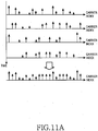
- FIGs. 11A and 11B illustrate the values of feedback calibration signals in the smart antenna system according to the present invention.
- a calibration signal is transmitted for a predetermined time of period and fed back.
- a signal can be calibrated across a total frequency band. Since the system knows the phase and amplitude of the transmitted calibration signal, it can compute calibration vectors by comparing the value of the transmitted calibration signal with that of the feedback calibration signal. Thus, the phase and amplitude of a signal can be calibrated using the calibration vectors. In the case where a small number of users are connected to a BS, this method is applicable.
- the calibration signal is not transmitted across the total frequency band and thus the values of feedback calibration signals are estimated by interpolation.
- This method is available when a large number of users are connected to the BS and more data carriers are needed.
- the system since the system knows the phase and amplitude of the transmitted calibration signal, it can compute calibration vectors by comparing the value of the transmitted calibration signal with that of the feedback calibration signal. Thus, the phase and amplitude of a signal can be calibrated using the calibration vectors.
- a calibration signal is allocated to the remaining carriers after allocating carriers to a data signal, prior to transmission in a smart antenna multicarrier communication system.
- the efficiency of frequency resources for data transmission is increased.
Landscapes
- Engineering & Computer Science (AREA)
- Computer Networks & Wireless Communication (AREA)
- Signal Processing (AREA)
- Radio Transmission System (AREA)
Claims (20)
- Système de communication à antenne intelligente comprenant :un ordonnanceur (412) pour attribuer un signal de données à une pluralité de porteuses comme porteuses de données, procurer le signal de données à un processeur de bande de base (411), et contrôler un processeur et contrôleur d'étalonnage (410) pour générer un signal d'étalonnage à attribuer à des porteuses de non-données auxquelles le signal de données n'est pas attribué ;le processeur et contrôleur d'étalonnage générant le signal d'étalonnage sur les porteuses de non-données sous contrôle de l'ordonnanceur, et calculant un vecteur d'étalonnage en utilisant le signal d'étalonnage et un signal d'étalonnage de rétroaction, qui est le signal d'étalonnage passé par un chemin de transmission ; etun processeur de bande de base (411) pour étalonner un vecteur de poids de formation de faisceau pour un signal de données avec le vecteur d'étalonnage et transmettre le signal de données étalonné dans le chemin de transmission ;caractérisé en ce queun seuil de temps est prédéterminé de telle sorte que, à moins qu'une porteuse spécifique à laquelle le signal d'étalonnage a été attribué ne comporte le signal d'étalonnage appliqué de nouveau sans dépasser ce seuil de temps, le signal d'étalonnage est attribué de force à la porteuse de telle sorte que le signal d'étalonnage est attribué périodiquement sur toute la bande de fréquence.
- Système de communication à antenne intelligente selon la revendication 1, dans lequel le processeur et contrôleur d'étalonnage comprend en outre :un générateur de signal d'étalonnage (413) pour générer le signal d'étalonnage sur les porteuses de non-données sous contrôle de l'ordonnanceur ; etun processeur de vecteur d'étalonnage (414) pour calculer le vecteur d'étalonnage en utilisant le signal d'étalonnage et le signal d'étalonnage de rétroaction.
- Système de communication à antenne intelligente selon la revendication 2, dans lequel le générateur de signal d'étalonnage comprend :un dispositif d'attribution de signal d'étalonnage (701) pour attribuer le signal d'étalonnage aux porteuses de non-données conformément à de l'information d'attribution de données de porteuse reçue de l'ordonnanceur ; etun premier processeur (702) à transformée de Fourier rapide inverse IFFT, soit Inverse Fast Fourier Transform, pour moduler le signal d'étalonnage reçu par l'IFFT en provenance du dispositif d'attribution de signal d'étalonnage.
- Système de communication à antenne intelligente selon la revendication 2 ou 3, dans lequel le processeur de vecteur d'étalonnage comprend :un processeur à transformée de Fourier rapide FFT, soit Fast Fourier Transform, pour séparer le signal d'étalonnage de rétroaction par porteuses ;un acquéreur de signal d'étalonnage (802) pour mesurer les phases et amplitudes du signal d'étalonnage sur les porteuses de non-données auxquelles le signal d'étalonnage est attribué, sur base d'information de position de porteuse d'étalonnage reçue de l'ordonnanceur ;un système d'actualisation de signal d'étalonnage (803) pour actualiser une mémoire avec les mesures de phase et d'amplitude ; etun calculateur de vecteur d'étalonnage (805) pour éliminer des caractéristiques de coupleur à partir des mesures de phase et d'amplitude stockées dans la mémoire et calculer un vecteur d'étalonnage en utilisant les caractéristiques de coupleur à partir de mesures de phase et d'amplitude.
- Système de communication à antenne intelligente selon la revendication 4, comprenant en outre un interpolateur (804) pour estimer les phases et amplitudes du signal d'étalonnage sur des porteuses auxquelles le signal d'étalonnage n'est pas attribué en interpolant les mesures de phase et d'amplitude stockées dans la mémoire, et stocker les phases et amplitudes évaluées du signal d'étalonnage dans la mémoire.
- Système de communication à antenne intelligente selon la revendication 1, dans lequel l'ordonnanceur comprend :un dispositif de découverte d'ensemble de porteuses (601) pour trouver des porteuses ayant des valeurs de temporisateur ne dépassant pas un seuil comme porteuses de données ;un dispositif d'attribution de données (603) pour attribuer le signal de données aux porteuses de données ; etun temporisateur (602) pour actualiser des valeurs de temporisateur pour les porteuses de données.
- Système de communication à antenne intelligente selon la revendication 1, dans lequel le processeur de bande de base comprend :un mappeur de données (504) pour recevoir le signal de données attribué aux porteuses de données par l'ordonnanceur ;un étalonneur (503) pour appliquer le vecteur d'étalonnage reçu du processeur de vecteur d'étalonnage au signal de données ; etun deuxième processeur IFFT (501) pour moduler le signal de données reçu par l'IFFT en provenance de l'étalonneur.
- Système de communication à antenne intelligente selon la revendication 1, dans lequel le système de communication à antenne intelligente est un système de communication à multiplexage par répartition orthogonale en fréquence OFDM, soit Orthogonal Frequency Division Multiplexing, ou à accès multiple par répartition orthogonale en fréquence OFDMA, soit Orthogonal Frequency Division Multiple Access.
- Système de communication à antenne intelligente comprenant :un ordonnanceur (412) pour contrôler un générateur de signal d'étalonnage pour générer un signal d'étalonnage à attribuer à des porteuses de non-données autres que des porteuses de données sur lesquelles un signal de données est reçu d'une station mobile ;un processeur et contrôleur d'étalonnage (410) pour étalonner le signal d'étalonnage sur les porteuses de non-données sous contrôle de l'ordonnanceur, et pour calculer un vecteur d'étalonnage en utilisant le signal d'étalonnage et un signal d'étalonnage de rétroaction, qui est le signal d'étalonnage passé par un chemin de réception ; etun processeur de bande de base (411) pour étalonner un vecteur de poids de formation de faisceau pour un signal de données avec le vecteur d'étalonnage et transmettre le signal de données étalonné dans le chemin de réception ;caractérisé en ce queun seuil de temps est prédéterminé de telle sorte que, à moins qu'une porteuse spécifique à laquelle le signal d'étalonnage a été attribué comporte le signal d'étalonnage appliqué de nouveau sans dépasser ce seuil de temps, le signal d'étalonnage est attribué de force à la porteuse de telle sorte que le signal d'étalonnage est attribué périodiquement sur toute la bande de fréquence.
- Système de communication à antenne intelligente selon la revendication 9, dans lequel le processeur et contrôleur d'étalonnage comprend :le générateur de signal d'étalonnage (413) pour générer le signal d'étalonnage sur les porteuses de non-données sous contrôle de l'ordonnanceur ; etun processeur de vecteur d'étalonnage (414) pour calculer le vecteur d'étalonnage en utilisant le signal d'étalonnage et le signal d'étalonnage de rétroaction.
- Système de communication à antenne intelligente selon la revendication 10, dans lequel le système de communication à antenne intelligente est un système de communication à multiplexage par répartition orthogonale en fréquence OFDM ou à accès multiple par répartition orthogonale en fréquence OFDMA.
- Procédé d'étalonnage de signal dans un système de communication à antenne intelligente, comprenant les étapes suivantes :attribution d'un signal de données à une pluralité de porteuses comme porteuses de données ;attribution d'un signal d'étalonnage pour des porteuses de non-données auxquelles le signal de données n'est pas attribué et transmission du signal d'étalonnage dans un chemin de transmission ;calcul d'un vecteur d'étalonnage en utilisant le signal d'étalonnage et d'un signal d'étalonnage de rétroaction reçu du chemin de transmission ; etétalonnage d'un vecteur de poids de formation de faisceau pour le signal de données en utilisant le vecteur d'étalonnage, et transmission du signal de données étalonné dans le chemin de transmission ;caractérisé en ce queun seuil de temps est prédéterminé de telle sorte que, à moins qu'une porteuse spécifique à laquelle le signal d'étalonnage a été attribué comporte le signal d'étalonnage appliqué de nouveau sans dépasser ce seuil de temps, le signal d'étalonnage est attribué de force à la porteuse de telle sorte que le signal d'étalonnage est attribué périodiquement sur toute la bande de fréquence.
- Procédé d'étalonnage de signal selon la revendication 12, dans lequel l'étape d'attribution et de transmission de signal d'étalonnage comprend :l'attribution du signal d'étalonnage aux porteuses de non-données ; etla modulation du signal d'étalonnage attribué.
- Procédé d'étalonnage de signal selon la revendication 12, dans lequel l'étape d'étalonnage et de transmission comprend :la réception du signal de données sur chacune des porteuses de données ;l'application du vecteur d'étalonnage au signal de données ; etla modulation du signal de données auquel le vecteur d'étalonnage est appliqué.
- Procédé d'étalonnage de signal selon la revendication 12 ou 13, dans lequel l'étape de calcul comprend les étapes suivantes :séparation du signal de rétroaction par des porteuses ;mesure des phases et amplitudes du signal d'étalonnage sur les porteuses de non-données auxquelles le signal d'étalonnage est attribué sur base d'information de position de porteuse d'étalonnage ;actualisation d'une mémoire avec les mesures de phase et d'amplitude ; etélimination de caractéristiques de coupleur des mesures de phase et d'amplitude stockées en mémoire et calcul d'un vecteur d'étalonnage en utilisant le caractéristiques de coupleur indépendamment des mesures de phase et d'amplitude.
- Procédé d'étalonnage de signal selon la revendication 15, dans lequel l'étape d'actualisation de mémoire comprend l'estimation des phases et amplitudes du signal d'étalonnage sur des porteuses auxquelles le signal d'étalonnage n'est pas attribué en interpolant les mesures de phase et d'amplitude stockées dans la mémoire, et le stockage des phases et amplitudes évaluées du signal d'étalonnage dans la mémoire.
- Procédé d'étalonnage de signal selon la revendication 12, dans lequel l'étape consistant à attribuer un signal d'étalonnage aux porteuses de non-données comprend en outre les étapes suivantes :comparaison d'une valeur de temporisateur de la nième porteuse à un seuil de temporisateur (Time_threshold) ;exclusion de la nième porteuse comme étant indisponible comme porteuse de données si la valeur de temporisateur de la nième porteuse est supérieure au seuil ;attribution de données sur la nième porteuse si la valeur de temporisateur de la nième porteuse n'est pas supérieure au seuil du temporisateur ;attribution d'un signal d'étalonnage sur la nième porteuse si des données ne sont pas attribuées à l'étape d'attribution de données.
- Procédé d'étalonnage de signal selon la revendication 12, dans lequel l'étape de calcul d'un vecteur d'étalonnage comprend en outre les étapes suivantes :réception d'un signal d'étalonnage de rétroaction sur une porteuse à laquelle est attribué un signal d'étalonnage ;actualisation d'une mémoire ayant les valeurs du signal d'étalonnage de rétroaction reçu sur des porteuses précédentes avec la valeur du signal d'étalonnage de rétroaction ;répétition de l'étape de réception et de l'étape d'actualisation pour toutes les porteuses d'un symbole ; etcalcul d'un vecteur d'étalonnage pour chacune des porteuses en utilisant les valeurs du signal d'étalonnage de rétroaction stocké dans la mémoire.
- Procédé d'étalonnage de signal selon la revendication 18, comprenant en outre l'élimination d'une caractéristique de coupleur parmi les valeurs du signal d'étalonnage de rétroaction stocké dans la mémoire et le calcul du vecteur d'étalonnage pour chaque porteuse.
- Procédé d'étalonnage de signal selon la revendication 18, comprenant en outre le calcul du vecteur d'étalonnage pour chaque porteuse en estimant les valeurs du signal d'étalonnage de rétroaction sur des porteuses auxquelles le signal de calibration n'est pas attribué.
Applications Claiming Priority (1)
| Application Number | Priority Date | Filing Date | Title |
|---|---|---|---|
| KR1020040100181A KR100633047B1 (ko) | 2004-12-02 | 2004-12-02 | 신호 보정 장치 및 방법을 구현하는 스마트 안테나 통신 시스템 |
Publications (2)
| Publication Number | Publication Date |
|---|---|
| EP1670094A1 EP1670094A1 (fr) | 2006-06-14 |
| EP1670094B1 true EP1670094B1 (fr) | 2017-05-31 |
Family
ID=35841700
Family Applications (1)
| Application Number | Title | Priority Date | Filing Date |
|---|---|---|---|
| EP05026272.4A Expired - Lifetime EP1670094B1 (fr) | 2004-12-02 | 2005-12-01 | Procédé de calibration d'un système d'antenne intelligente |
Country Status (5)
| Country | Link |
|---|---|
| US (1) | US7801564B2 (fr) |
| EP (1) | EP1670094B1 (fr) |
| JP (1) | JP4455483B2 (fr) |
| KR (1) | KR100633047B1 (fr) |
| CN (1) | CN1783748B (fr) |
Families Citing this family (27)
| Publication number | Priority date | Publication date | Assignee | Title |
|---|---|---|---|---|
| US7652577B1 (en) | 2006-02-04 | 2010-01-26 | Checkpoint Systems, Inc. | Systems and methods of beamforming in radio frequency identification applications |
| US7873326B2 (en) | 2006-07-11 | 2011-01-18 | Mojix, Inc. | RFID beam forming system |
| KR101009781B1 (ko) * | 2006-07-11 | 2011-01-19 | 삼성전자주식회사 | 통신 시스템에서 캘리브레이션 장치 및 방법 |
| EP2067278B1 (fr) * | 2006-08-22 | 2016-06-15 | Koninklijke Philips N.V. | Procede pour transmettre des donnees dans un systeme mobile et stations radio pour ceux-ci |
| US20080207258A1 (en) * | 2007-02-26 | 2008-08-28 | Broadcom Corporation, A California Corporation | Multimode transmitter with digital up conversion and methods for use therewith |
| US20090093222A1 (en) | 2007-10-03 | 2009-04-09 | Qualcomm Incorporated | Calibration and beamforming in a wireless communication system |
| CN101414875B (zh) * | 2007-10-15 | 2013-06-26 | 中国移动通信集团上海有限公司 | 时分双工系统中对隧道进行覆盖的方法、设备和系统 |
| WO2009093233A2 (fr) * | 2008-01-22 | 2009-07-30 | Provigent Ltd. | Mise en forme de faisceaux dans des systèmes de communication mimo |
| KR101452999B1 (ko) * | 2008-01-25 | 2014-10-21 | 삼성전자주식회사 | 다중 안테나 시스템에서 캘리브레이션 장치 및 방법 |
| US8217760B2 (en) * | 2008-03-20 | 2012-07-10 | Checkpoint Systems, Inc. | Applique nodes for performance and functionality enhancement in radio frequency identification systems |
| WO2009151778A2 (fr) | 2008-04-14 | 2009-12-17 | Mojix, Inc. | Système et procédé d’estimation et de suivi d’emplacement d’étiquettes d’identification par radiofréquence |
| CN101304276B (zh) * | 2008-06-30 | 2012-07-04 | 华为技术有限公司 | 一种发射通道校正的方法及系统 |
| JP2010021784A (ja) * | 2008-07-10 | 2010-01-28 | Sony Corp | 通信装置及び通信校正方法 |
| US8786440B2 (en) * | 2009-10-02 | 2014-07-22 | Checkpoint Systems, Inc. | Calibration of beamforming nodes in a configurable monitoring device system |
| CN101951618A (zh) * | 2010-08-31 | 2011-01-19 | 芯通科技(成都)有限公司 | Rru自动定标与测试系统 |
| EP2602867B1 (fr) | 2010-09-08 | 2014-11-12 | Huawei Technologies Co., Ltd. | Procédé, dispositif et système d'étalonnage de voie |
| JP5599353B2 (ja) * | 2011-03-30 | 2014-10-01 | パナソニック株式会社 | 送受信装置 |
| US9178737B2 (en) * | 2012-11-20 | 2015-11-03 | Intel Deutschland Gmbh | Method for generating an OFDM data signal |
| WO2014117341A1 (fr) * | 2013-01-30 | 2014-08-07 | Telefonaktiebolaget L M Ericsson (Publ) | Procédé et appareil pour étalonner de multiples antennes |
| US9596676B2 (en) * | 2013-02-13 | 2017-03-14 | Qualcomm Incorporated | Calibration of a downlink transmit path of a base station |
| US20140329472A1 (en) * | 2013-05-03 | 2014-11-06 | CommSense LLC | Antenna Environment Sensing Device |
| US9883337B2 (en) | 2015-04-24 | 2018-01-30 | Mijix, Inc. | Location based services for RFID and sensor networks |
| JP2018019374A (ja) | 2016-07-29 | 2018-02-01 | 富士通株式会社 | 基地局およびアンテナキャリブレーション方法 |
| US10326538B2 (en) * | 2017-04-05 | 2019-06-18 | Cisco Technology, Inc. | Remote radio head reciprocity calibration |
| JP2019114961A (ja) * | 2017-12-25 | 2019-07-11 | 富士通株式会社 | 無線通信装置、及びアンテナキャリブレーション方法 |
| EP3809605A4 (fr) * | 2018-07-24 | 2021-06-30 | Mitsubishi Electric Corporation | Dispositif d'étalonnage et procédé d'étalonnage d'antenne réseau, antenne réseau et programme |
| KR102195541B1 (ko) * | 2018-08-10 | 2020-12-28 | 주식회사 다빈시스템스 | 다중 rf 채널 시스템의 캘리브레이션 방법 및 장치 |
Family Cites Families (19)
| Publication number | Priority date | Publication date | Assignee | Title |
|---|---|---|---|---|
| GB2285537B (en) * | 1989-09-28 | 1995-11-08 | Marconi Co Ltd | Calibration of distributed receiver system for antenna array |
| GB2313523B (en) | 1996-05-23 | 2000-06-07 | Motorola Ltd | Self-calibration apparatus and method for communication device |
| JP3369466B2 (ja) | 1997-03-18 | 2003-01-20 | 松下電器産業株式会社 | アレーアンテナ無線受信装置のキャリブレーション装置 |
| US6208287B1 (en) * | 1998-03-16 | 2001-03-27 | Raytheoncompany | Phased array antenna calibration system and method |
| ID27970A (id) * | 1998-08-05 | 2001-05-03 | Sanyo Electric Co | Radas radio dan metode kalibrasi untuk itu |
| US6184829B1 (en) * | 1999-01-08 | 2001-02-06 | Trueposition, Inc. | Calibration for wireless location system |
| HK1047001B (zh) | 1999-03-30 | 2005-06-03 | 三洋电机株式会社 | 无线装置及其天线方向性的校准方法 |
| JP2003218621A (ja) | 2002-01-21 | 2003-07-31 | Nec Corp | アレーアンテナの校正装置及び校正方法 |
| JP3769513B2 (ja) * | 2002-03-19 | 2006-04-26 | 株式会社東芝 | アレイアンテナ装置 |
| JP4010225B2 (ja) | 2002-10-30 | 2007-11-21 | 日本電気株式会社 | アレーアンテナ送受信装置 |
| KR100608736B1 (ko) * | 2003-04-29 | 2006-08-04 | 엘지전자 주식회사 | 스마트 안테나 시스템의 기준신호 발생장치 |
| JP4388303B2 (ja) | 2003-05-16 | 2009-12-24 | 日本無線株式会社 | アレイアンテナ通信装置 |
| DE602004029906D1 (de) * | 2003-08-27 | 2010-12-16 | Wavion Ltd | Wlan-kapazitäts-erweiterung durch verwendung von sdm |
| KR100675489B1 (ko) * | 2004-11-23 | 2007-01-29 | 삼성전자주식회사 | 신호 보정 장치 및 방법을 구현하는 멀티 안테나 통신 시스템 |
| US7362266B2 (en) * | 2004-12-07 | 2008-04-22 | Lockheed Martin Corporation | Mutual coupling method for calibrating a phased array |
| US7408507B1 (en) * | 2005-03-15 | 2008-08-05 | The United States Of America As Represented By The Secretary Of The Navy | Antenna calibration method and system |
| US8498669B2 (en) * | 2005-06-16 | 2013-07-30 | Qualcomm Incorporated | Antenna array calibration for wireless communication systems |
| US9118111B2 (en) * | 2005-11-02 | 2015-08-25 | Qualcomm Incorporated | Antenna array calibration for wireless communication systems |
| US8280430B2 (en) * | 2005-11-02 | 2012-10-02 | Qualcomm Incorporated | Antenna array calibration for multi-input multi-output wireless communication systems |
-
2004
- 2004-12-02 KR KR1020040100181A patent/KR100633047B1/ko not_active Expired - Fee Related
-
2005
- 2005-12-01 EP EP05026272.4A patent/EP1670094B1/fr not_active Expired - Lifetime
- 2005-12-02 JP JP2005349969A patent/JP4455483B2/ja not_active Expired - Fee Related
- 2005-12-02 US US11/293,564 patent/US7801564B2/en not_active Expired - Fee Related
- 2005-12-02 CN CN2005101310133A patent/CN1783748B/zh not_active Expired - Fee Related
Also Published As
| Publication number | Publication date |
|---|---|
| US20060135211A1 (en) | 2006-06-22 |
| JP2006166452A (ja) | 2006-06-22 |
| EP1670094A1 (fr) | 2006-06-14 |
| CN1783748B (zh) | 2010-05-12 |
| CN1783748A (zh) | 2006-06-07 |
| JP4455483B2 (ja) | 2010-04-21 |
| KR100633047B1 (ko) | 2006-10-11 |
| US7801564B2 (en) | 2010-09-21 |
| KR20060061443A (ko) | 2006-06-08 |
Similar Documents
| Publication | Publication Date | Title |
|---|---|---|
| EP1670094B1 (fr) | Procédé de calibration d'un système d'antenne intelligente | |
| EP1438768B1 (fr) | Etalonnage en fonction de la frequence d'un systeme radio large bande utilisant des canaux a bande etroite | |
| EP1433271B1 (fr) | Calibrage d'un systeme de radiocommunication | |
| KR100656979B1 (ko) | 스마트 안테나 어레이 시스템의 실시간 교정 방법 | |
| US10734722B2 (en) | Beamforming method, apparatus for polarized antenna array and radio communication device and system thereof | |
| US8208963B2 (en) | Communication method and system | |
| US6400318B1 (en) | Adaptive array antenna | |
| CN102835039B (zh) | 通信方法和通信系统 | |
| US6496140B1 (en) | Method for calibrating a smart-antenna array radio transceiver unit and calibrating system | |
| EP1708385A2 (fr) | Appareil d'étalonnage d'un réseau d'antennes | |
| US8886254B2 (en) | Radio base station and antenna weight setting method | |
| EP2533360B1 (fr) | Procédé et dispositif pour l'étalonnage d'une antenne | |
| KR20030089215A (ko) | 이동통신시스템에서 스마트 안테나의 순방향 송신빔 형성장치 및 방법 | |
| US20100118745A1 (en) | Wireless communication apparatus | |
| EP3427398B1 (fr) | Procédé et appareil de sondage de canal destinés à un réseau de communication sans fil mu-mimo | |
| US8219035B2 (en) | Enhanced calibration for multiple signal processing paths in a wireless network | |
| US7389193B2 (en) | Apparatus and method for calibrating transmission paths in a multicarrier communication system using multiple antennas | |
| EP1143559B1 (fr) | Dispositif adaptatif de correction de phase pour produire une configuration directionnelle et procede de correction | |
| EP1093186B1 (fr) | Radioemetteur et procede de reglage de la directivite d'emission | |
| WO2017153732A1 (fr) | Procédé et appareil de sondage de canal destinés à un réseau de communication sans fil mu-mimo | |
| KR20070066430A (ko) | 스마트 안테나 시스템의 송수신 경로 보정 장치 | |
| AU2002362566A1 (en) | Frequency dependent calibration of a wideband radio system using narrowband channels | |
| AU2002362567A1 (en) | Calibration of a radio communications system |
Legal Events
| Date | Code | Title | Description |
|---|---|---|---|
| PUAI | Public reference made under article 153(3) epc to a published international application that has entered the european phase |
Free format text: ORIGINAL CODE: 0009012 |
|
| AK | Designated contracting states |
Kind code of ref document: A1 Designated state(s): AT BE BG CH CY CZ DE DK EE ES FI FR GB GR HU IE IS IT LI LT LU LV MC NL PL PT RO SE SI SK TR |
|
| AX | Request for extension of the european patent |
Extension state: AL BA HR MK YU |
|
| 17P | Request for examination filed |
Effective date: 20060523 |
|
| 17Q | First examination report despatched |
Effective date: 20060721 |
|
| AKX | Designation fees paid |
Designated state(s): DE FR GB IT SE |
|
| RAP1 | Party data changed (applicant data changed or rights of an application transferred) |
Owner name: SAMSUNG ELECTRONICS CO., LTD. |
|
| GRAP | Despatch of communication of intention to grant a patent |
Free format text: ORIGINAL CODE: EPIDOSNIGR1 |
|
| INTG | Intention to grant announced |
Effective date: 20161209 |
|
| RIN1 | Information on inventor provided before grant (corrected) |
Inventor name: YANG, JANG-HOON Inventor name: CHAE, HEON-KI Inventor name: KWON, YOUNG-HOON |
|
| GRAS | Grant fee paid |
Free format text: ORIGINAL CODE: EPIDOSNIGR3 |
|
| GRAA | (expected) grant |
Free format text: ORIGINAL CODE: 0009210 |
|
| AK | Designated contracting states |
Kind code of ref document: B1 Designated state(s): DE FR GB IT SE |
|
| REG | Reference to a national code |
Ref country code: GB Ref legal event code: FG4D |
|
| REG | Reference to a national code |
Ref country code: DE Ref legal event code: R096 Ref document number: 602005052026 Country of ref document: DE |
|
| REG | Reference to a national code |
Ref country code: FR Ref legal event code: PLFP Year of fee payment: 13 |
|
| PG25 | Lapsed in a contracting state [announced via postgrant information from national office to epo] |
Ref country code: SE Free format text: LAPSE BECAUSE OF FAILURE TO SUBMIT A TRANSLATION OF THE DESCRIPTION OR TO PAY THE FEE WITHIN THE PRESCRIBED TIME-LIMIT Effective date: 20170531 |
|
| PG25 | Lapsed in a contracting state [announced via postgrant information from national office to epo] |
Ref country code: IT Free format text: LAPSE BECAUSE OF FAILURE TO SUBMIT A TRANSLATION OF THE DESCRIPTION OR TO PAY THE FEE WITHIN THE PRESCRIBED TIME-LIMIT Effective date: 20170531 |
|
| REG | Reference to a national code |
Ref country code: DE Ref legal event code: R097 Ref document number: 602005052026 Country of ref document: DE |
|
| PLBE | No opposition filed within time limit |
Free format text: ORIGINAL CODE: 0009261 |
|
| STAA | Information on the status of an ep patent application or granted ep patent |
Free format text: STATUS: NO OPPOSITION FILED WITHIN TIME LIMIT |
|
| 26N | No opposition filed |
Effective date: 20180301 |
|
| GBPC | Gb: european patent ceased through non-payment of renewal fee |
Effective date: 20171201 |
|
| PG25 | Lapsed in a contracting state [announced via postgrant information from national office to epo] |
Ref country code: GB Free format text: LAPSE BECAUSE OF NON-PAYMENT OF DUE FEES Effective date: 20171201 |
|
| PGFP | Annual fee paid to national office [announced via postgrant information from national office to epo] |
Ref country code: DE Payment date: 20181205 Year of fee payment: 14 |
|
| PGFP | Annual fee paid to national office [announced via postgrant information from national office to epo] |
Ref country code: FR Payment date: 20181122 Year of fee payment: 14 |
|
| REG | Reference to a national code |
Ref country code: DE Ref legal event code: R119 Ref document number: 602005052026 Country of ref document: DE |
|
| PG25 | Lapsed in a contracting state [announced via postgrant information from national office to epo] |
Ref country code: DE Free format text: LAPSE BECAUSE OF NON-PAYMENT OF DUE FEES Effective date: 20200701 Ref country code: FR Free format text: LAPSE BECAUSE OF NON-PAYMENT OF DUE FEES Effective date: 20191231 |