EP1672506A2 - Système informatique à tolérance de pannes et son procédé de synchronisation - Google Patents
Système informatique à tolérance de pannes et son procédé de synchronisation Download PDFInfo
- Publication number
- EP1672506A2 EP1672506A2 EP05112092A EP05112092A EP1672506A2 EP 1672506 A2 EP1672506 A2 EP 1672506A2 EP 05112092 A EP05112092 A EP 05112092A EP 05112092 A EP05112092 A EP 05112092A EP 1672506 A2 EP1672506 A2 EP 1672506A2
- Authority
- EP
- European Patent Office
- Prior art keywords
- computer system
- data
- address
- write
- main memory
- Prior art date
- Legal status (The legal status is an assumption and is not a legal conclusion. Google has not performed a legal analysis and makes no representation as to the accuracy of the status listed.)
- Withdrawn
Links
Images



Classifications
-
- G—PHYSICS
- G06—COMPUTING OR CALCULATING; COUNTING
- G06F—ELECTRIC DIGITAL DATA PROCESSING
- G06F11/00—Error detection; Error correction; Monitoring
- G06F11/07—Responding to the occurrence of a fault, e.g. fault tolerance
- G06F11/16—Error detection or correction of the data by redundancy in hardware
- G06F11/1658—Data re-synchronization of a redundant component, or initial sync of replacement, additional or spare unit
Definitions
- the present invention relates to a fault tolerant computer system of lockstep type and a synchronization method for the same in which a plurality of computer systems simultaneously execute the same instruction string at timing synchronized with a clock signal, and in particular, to a fault tolerant computer system of lockstep type and a synchronization method for the same in which operation activated, when the operational synchronism (a lockstep state) between the computer systems is disturbed in a first computer system, to restore the operational synchronism (to rebuild the lockstep state) can be conducted without stopping the ordinary operation of computer systems other than the first computer system separated from the fault tolerant computer system.
- the lockstep fault tolerant computer system of the related art in a plurality of computer systems synchronously executing the same instruction string, when it is detected that one of the computer systems conducts an output operation different from that of the other computer systems due to failure or external or internal factors, the computer system in which the fault takes place is once separated from the other computer systems to be set to a non-operating state.
- the computer system is replaced with another system if necessary depending on the factor of the fault. If the replacement of the computer system is not required, the system is, for example, re-initialized according to necessity and is set again to an operative state.
- the contents of the memory of the failed computer thus replaced or the memory of a computer on the standby side in the initial setup phase is required to be set to match those of an associated computer on the active side. Therefore, it is required to copy the entire data of the main memory of the computer system in an operative state onto the main memory of the computer system to be restored to an operative state.
- a first object of the present invention which has been devised to solve the above problem, to accomplish the processing to restore the computer system on the standby side without stopping operation of the computer systems on the active side.
- a second object of the present invention is to remove the requirement of the particular processing for the software.
- a third object of the present invention is to suppress the deterioration in the performance of the computer systems on the active side during the restoration of the computer on the standby side.
- a fourth object of the present invention is to complete the data transfer through a possibly small number of processing steps to thereby implement the synchronization of the computer systems in a short period of time.
- a fault tolerant computer system including a plurality of computer systems each of which includes one processor or a plurality of processors, a main memory, a routine controller, a synchronization (sync) controller, and a bridge circuit connecting the processors, the main memory, the routine controller, and the sync controller to each other to control the constituent components.
- the respective computer systems are synchronized and process the same instruction string.
- the routing controller includes a memory access monitor unit including a counter module which determines, when the data is read via the sync controller from the main memory, a state of a process of the read operation and an address comparator to compare, when the processor issues a write instruction, a counter value of the counter module with an address (a write address) for which a writing operation is conducted by the write instruction.
- a memory access monitor unit including a counter module which determines, when the data is read via the sync controller from the main memory, a state of a process of the read operation and an address comparator to compare, when the processor issues a write instruction, a counter value of the counter module with an address (a write address) for which a writing operation is conducted by the write instruction.
- the processor issues a write instruction for the main memory during an operation in which to synchronize a computer system in a non-operating state (a standby computer system) with a computer system in an operating state (an active computer system), data of the main memory of the active computer system is sequentially transferred to the standby computer system; the memory access monitor unit transfers, according to a result of a comparison conducted by the address comparator, to the sync controller of the active computer system only write data of an address for which a data read operation has already been completed and write data of an address for which a data read operation is being currently conducted.
- a fault tolerant computer system to achieve the object.
- the system includes a plurality of computer systems each of which includes one processor or a plurality of processors, a main memory, a routine controller, a sync controller, and a bridge circuit connecting the processors, the main memory, the routine controller, and the sync controller to each other to control the constituent components.
- the respective computer systems are synchronized and process the same instruction string.
- the routing controller includes a memory access monitor unit including a counter module which determines, when the data is read via the sync controller from the main memory, a state of a process of the read operation and an address comparator to compare, when the processor issues a write instruction, a counter value of the counter module with an a write address for which a writing operation is conducted by the write instruction.
- the processor issues a write instruction for the main memory during an operation in which to synchronize a standby computer system with an active computer system, data of the main memory of the active computer system is sequentially transferred to the standby computer system; the memory access monitor unit executes, if the write instruction is issued for an address for which a data read operation is completed or for which a data read operation is currently in process according to a result of a comparison conducted by the address comparator, the write instruction and notifies an interrupt, and the sync controller obtains the write data in an operation of executing interrupt processing of the interrupt thus notified.
- a synchronization method of synchronizing a standby computer system with an active computer system for use with a fault tolerant computer system including a plurality of computer systems each of which includes one processor or a plurality of processors, a main memory, a routine controller, a sync controller, and a bridge circuit connecting the processors, the main memory, the routine controller, and the sync controller to each other to control the constituent components.
- the respective computer systems are synchronized and process the same instruction string.
- the standby-side computer system can be synchronized without stopping operation of the active-side computers, namely, by retaining the ordinary operation state.
- a second advantage is that on the active side, the write access of any computer system to the main memory is not limited for the software. Therefore, the memory access is not particularly taken into consideration for the software.
- the computer In the synchronizing operation, the computer can be used in almost the same way as in the ordinary operation. This makes it possible to retain simplicity of software control.
- a third advantage is that since the memory access is not limited for software and firmware, the performance reduction of the computer systems is limited to the memory access for the synchronization processing. Therefore, the synchronization can be completely accomplished in a remarkably shorter period of time as compared with the case in which the memory accesses are inhibited in the computer systems.
- a fourth advantage is that even if a write instruction is issued for a main memory during the synchronization processing, duplicated transfers of write data of the write instruction to an associated computer system on the standby side can be reduced to the maximum extent. This consequently suppresses deterioration in the system performance as much as possible.
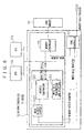
- Fig. 1 is a block diagram showing a general configuration of a first embodiment in accordance with the present invention.
- a line connecting constituent components to each other is a bus or wiring, and an arrow indicates a direction of propagation of a signal.
- FIGS. 2 and 6 This also applies to FIGS. 2 and 6.
- the system 100 includes a computer system 101 and a computer system 102 which are substantially equal in structure to each other.
- the embodiment includes two computer systems
- the fault tolerant computer system may include three or more computer systems.
- the computer systems 101 and 102 respectively include central processing units (CPUs) 10 1 and 10 2 , and CPUs 20 1 and 20 2 .
- CPUs central processing units
- each computer system includes two CPUs, the computer system may also includes one CPU or more than three CPUs.
- the CPUs 10 1 and 10 2 (20 1 , 20 2 ) are connected via a bridge circuit 11 (21) to a routing controller 12 (22).
- the bridge circuit 11 (21) includes a routing controller 12 (22), a sync controller 13 (23), and an input-output (IO) controller 14 (24).
- the routing controller 12 (22) is linked with a main memory 15 (25).
- the IO controller 14 (24) is coupled with IO units 16 and 17 (26, 27).
- the computer systems 101 and 102 are synchronized with each other to conduct substantially the same operation. That is, the computer systems 101 and 102 operate according to the same clock signal.
- the CPUs 10 1 and 10 2 and the CPUs 20 1 and 20 2 simultaneously issue the same instructions, respectively.
- the instructions are delivered respectively to the bridge circuits 11 and 21.
- the CPUs access to the main memories 15 and 25 respectively, via the bridge circuits 11 and 21. Also, this leads to control operations for the IO units 16 and 17 and the IO units 26 and 27.
- Part of the instructions issued from the CPUs 10 1 and 10 2 of the computer system 101 are fed via the routing control module 12 to the sync controller 23 of the computer system 102.
- the same instructions are also issued from the CPUs 20 1 and 20 2 , which are transmitted via the routing controller 22 to the sync controller 13.
- the sync controller 23 acknowledges difference in timing between the instructions issued from the CPUs.
- the sync controller 13 acknowledges difference in timing between the instructions issued from the CPUs.
- FIG. 2 shows the configuration of the bridge circuit 11 of FIG. 1 in more detail.
- the routine controller 12 includes a memory controller 121 to control access to the main memory 15, and a memory access monitor module 122.
- the routing controller 12 includes other controllers such as a bus controller, such constituent components are not shown.
- the memory access monitor module 122 includes a read request counter 1223 of which a count value is increased each time the sync controller 13 issues a read request to the memory controller 121, a read end counter 1224 of which a count value is incremented each time the read operation is completed, a a address comparator 1221 to compare the count value of the request counter 1223 with that of the end counter 1224, and a write data transmission and reception unit 1222 to transfer write data to the sync controller 13.
- data can be transferred in an ascending order or in a descending order, data is transferred in an ascending order in the present specification for convenience of description.
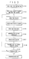
- the flowchart of FIG. 3 shows a flow of a procedure to transfer data of the main memory 15 to the computer system 102 to restore the computer system 102 in the fault tolerant computer system 100.
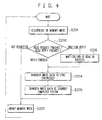
- the flowchart shown in Fig. 4 is a procedure of processing when a memory write instruction is issued during the memory copy process.
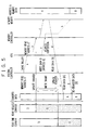
- the flowchart of Fig. 5 shows a flow of instructions and data in the operation to transfer data from the main memory 15 to the computer system 102.
- the read request and end counters 1223 and 1224 have a counter value of "five". This indicates that data of address 6 is being transferred.
- FIGS. 3 to 5 description will be given of the procedure of synchronization of computer systems in a second embodiment of the fault tolerant computer system 100.
- the computer system 101 is assumed to be an active side and the computer system 102 a standby side, the roles of the computer systems 101 and 102 may be exchanged.
- the routing controller 12 inquires of the CPU whether or not the CPU has data of address 6 in a cache thereof (a in FIG. 5).
- the routing controller 12 issues a read request to the memory controller 121 (b in FIG. 5).
- the read request counter 1223 is updated at step S104 and the main memory read operation is initiated (c in FIG. 5).
- a read reply is sent out at step S105 (d in FIG. 5)
- the read data is transferred to the sync controller 13 at step S106.
- the read end counter 1224 is then updated at step S107, and thereafter the read data is delivered to the sync controller 23 of the computer system 102 at step S108 (e in FIG. 5).
- a check is made at step S109 to determine whether or not the data of the entire area of the main memory 15 has been completely transferred.
- step S109 If there still remains data to be transferred, control returns to step S103 to repeatedly execute the above processing. If it is determined at step S109 that the overall data has been transferred, it is assumed that the synchronization has been finished and hence the memory copy is terminated.
- the fault tolerant computer system 100 starts its ordinary operation using the computer systems 101 and 102.
- steps S106 and S107 of the flowchart shown in FIG. 3 may be exchanged or may be simultaneously executed.
- the memory write instruction from the CPU takes precedence in execution over the memory read instruction from the sync controller 13. Consequently, it is not required to consider the problem that the data at an address where a memory read operation has been conducted is changed by a memory write instruction.
- a memory write instruction is issued for the address of the read request, there possibly occurs a case that the data of the address for which a read reply has been made is changed by a writing operation.
- the memory write instruction is temporarily stopped for an address for which a read request has been issued during the period of time.
- a write address thereof is passed to the address comparator 1221.
- a check is made at step S202 to determine whether or not the write address is the address of the read request from the sync controller 13.
- the address comparator 1221 compares the write address with the counter value of the read request counter 1223 and that of the read end counter 1224. If the write address is more than the counter value of the request counter 1223, it is assumed that the address of the write instruction has not been used by any read request.
- a memory write grant is given to the memory controller 121 at step S203 and then the process returns to the wait state.
- the address comparator 1221 determines at step S202 that the write address is equal to or less than the count value of the read end counter 1224, it is assumed that the write instruction is issued for an address for which the memory copy has been finished.
- the write data is delivered via the write data transmission and reception module 1222 to the sync controller 13 at step S204.
- the sync controller 13 sends the write data to the sync controller 23 of the computer system 102 at step S205.
- the sync controller 13 then gives a memory write grant to the memory controller 122 at step S203 and returns to the wait state.
- step S202 When the address comparator 1221 detects at step S202 that the write address is equal to the counter value of the read request counter 1223 and is more than that of the read end counter 1224, it is assumed that the write instruction is issued for an address for which a memory read operation is currently in process. Therefore, control waits at step S206 for an event in which the count value of the end counter 1224 is updated and then goes to step S204. Assume that the read request counter 1223 has a count value of five and the read end counter 1224 has a count value of six. When a write instruction (with data B) is issued as indicated by f in FIG. 5, the process waits for an event in which the read end counter 1224 is updated.
- the data is fed via the transmission and reception unit 1222 and the sync controller 13 to the sync controller 23 of the computer system 102 as indicated by g in FIG. 5 (steps S204 and S205). Accordingly, the system gives a memory write grant to the memory controller 121 at step S203 (a memory writing operation is performed as denoted by h in FIG. 5) and then returns to the wait state.
- Fig. 6 shows in a block diagram a configuration of a second embodiment of the bridge circuit 11 in accordance with the present invention.
- the overall configuration of the second embodiment is substantially equal to that of the first embodiment.
- the constituent components equivalent to those of the first embodiment of FIG. 2 are assigned with the same reference numerals, and hence duplicated description of the bridge circuit 11 will be avoided.
- the read end counter is not used and only the read request counter 1223 is employed.
- Fig. 7 shows a procedure to deliver data from the main memory 15 to the computer system 102 acting as the standby side in the second embodiment.
- step S301 When the CPU of the computer system 101 issues at step S301 a synchronization start instruction to the sync controller 13, the read request counter 1223 is reset at step S302. The sync controller 13 then issues a read request to the memory controller 121 at step S303. The read request counter 1223 is updated at step S304 and the memory read operation is started. When a read data reply is made at step S305, the read data is fed to the sync controller 13 at step S306. The read data is then transferred at step S307 to the sync controller 23 of the computer system 102. A check is made at step S308 to determine whether or not an interrupt has been notified. If the interrupt has not been notified, a check is made at step S310 to determine whether or not the data of the entire area of the main memory 15 has been transferred. If there remains data to be transferred, control returns to step S303 to execute again the processing described above.
- step S308 If it is determined at step S308 that the interrupt has been notified, control goes to step S309 to execute interrupt processing.
- write data is delivered at step S3091 via the write data transmission and reception module 1222 to the sync controller 13.
- the write data is transferred at step 3092 to the sync controller 23 of the computer system 102 to thereby terminate the interrupt processing. If it is detected at step S310 that the data of the main memory 15 has been completely transferred, the system assumes that the synchronization is finished and terminates the copy processing.
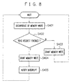
- Fig. 8 shows in a flowchart a procedure of processing in the bridge circuit 11 when a memory write instruction is issued during a memory copy process.
- the wait state when the CPU issues at step S401 a memory write instruction to the memory controller 121, a write address of the instruction is fed to the address comparator 1221.
- the comparator 1221 makes a check at step S402 to determine whether or not the address has already been requested by the sync controller 13 for a read request.
- the comparator 1221 compares the write address with the counter value of the read request counter 1223.
- the comparator 1221 assumes that the address of the write request has not been designated by a read request and permits at step S403 a memory write to the memory controller 121 to thereafter return to the wait state. If the comparator 1221 determines at step S402 that the write address is equal to or less than the counter value of the counter 1223, the comparator 1221 assumes that the write request has been issued for an address which has already been designated by a read request. Therefore, the address comparator 1221 gives at step S403 a memory write grant to the memory controller 121 and notifies an interrupt at step S405 to return to the wait state.
- the steps S404 and S405 may be exchanged in the execution order or may be simultaneously executed.
- the second embodiment includes only the read request counter
- the embodiment includes only the read end counter by removing the read request counter.
- the method described above is carried out by adding one to the counter value of the read end counter.
- An embodiment of the present invention may be summarised as follows. Each time a sync controller sequentially issues a read request to a memory controller, a count value of a first counter is incremented. When a read operation is conducted for the read request, a count value of a second counter is incremented and the data is transferred to a standby computer. If a memory write instruction is issued during a memory copy operation, an address comparator compares a write address of the memory write instruction with the count values of the first and second counters. If the write address is more than the count values, the memory write operation is permitted. If the write address is equal to the count value of the first counter, the process waits for termination of the data read operation. Otherwise, the write operation is immediately permitted and the write data is transferred to the sync controller. Data of a memory on the active side can be hence copied onto the standby computer without stopping the system operation.
Landscapes
- Engineering & Computer Science (AREA)
- Theoretical Computer Science (AREA)
- Quality & Reliability (AREA)
- Physics & Mathematics (AREA)
- General Engineering & Computer Science (AREA)
- General Physics & Mathematics (AREA)
- Hardware Redundancy (AREA)
- Memory System (AREA)
Applications Claiming Priority (1)
| Application Number | Priority Date | Filing Date | Title |
|---|---|---|---|
| JP2004365345A JP4161276B2 (ja) | 2004-12-17 | 2004-12-17 | フォルトトレラントコンピュータ装置およびその同期化方法 |
Publications (2)
| Publication Number | Publication Date |
|---|---|
| EP1672506A2 true EP1672506A2 (fr) | 2006-06-21 |
| EP1672506A3 EP1672506A3 (fr) | 2006-07-05 |
Family
ID=36018673
Family Applications (1)
| Application Number | Title | Priority Date | Filing Date |
|---|---|---|---|
| EP05112092A Withdrawn EP1672506A3 (fr) | 2004-12-17 | 2005-12-14 | Système informatique à tolérance de pannes et son procédé de synchronisation |
Country Status (6)
| Country | Link |
|---|---|
| US (1) | US7493517B2 (fr) |
| EP (1) | EP1672506A3 (fr) |
| JP (1) | JP4161276B2 (fr) |
| CN (1) | CN1790285A (fr) |
| AU (1) | AU2005244590A1 (fr) |
| CA (1) | CA2530013A1 (fr) |
Cited By (1)
| Publication number | Priority date | Publication date | Assignee | Title |
|---|---|---|---|---|
| EP2849005A4 (fr) * | 2012-05-10 | 2016-07-06 | Mitsubishi Electric Corp | Système redondant double de veille |
Families Citing this family (12)
| Publication number | Priority date | Publication date | Assignee | Title |
|---|---|---|---|---|
| EP1629614A1 (fr) * | 2003-05-20 | 2006-03-01 | Philips Intellectual Property & Standards GmbH | Systeme de communication a declenchement temporel et procede de synchronisation d'un reseau bicanal |
| DE102006056879A1 (de) * | 2006-12-01 | 2008-06-05 | Dürr Systems GmbH | Fehlerprotokollierungsverfahren für eine Beschichtungsanlage |
| JP5153310B2 (ja) * | 2007-12-10 | 2013-02-27 | 株式会社日立製作所 | フォールトトレラントコンピュータシステム、並びに再同期稼働化処理方法、及びプログラム |
| JP5206009B2 (ja) * | 2008-02-18 | 2013-06-12 | 日本電気株式会社 | フォルトトレラントコンピュータ、同期制御方法、及びプログラム |
| JP5481889B2 (ja) * | 2009-03-11 | 2014-04-23 | 日本電気株式会社 | フォールトトレラントコンピュータ、その同期制御方法及びコンピュータプログラム |
| CN104699550B (zh) * | 2014-12-05 | 2017-09-12 | 中国航空工业集团公司第六三一研究所 | 一种基于lockstep架构的错误恢复方法 |
| JP6083480B1 (ja) * | 2016-02-18 | 2017-02-22 | 日本電気株式会社 | 監視装置、フォールトトレラントシステムおよび方法 |
| JP6090492B1 (ja) | 2016-03-18 | 2017-03-08 | 日本電気株式会社 | メモリアクセス制御装置、情報処理システム、メモリアクセス制御方法、及び、プログラム |
| US10515671B2 (en) | 2016-09-22 | 2019-12-24 | Advanced Micro Devices, Inc. | Method and apparatus for reducing memory access latency |
| CN109358812A (zh) * | 2018-10-09 | 2019-02-19 | 郑州云海信息技术有限公司 | 一种集群系统中io请求的处理方法、装置及相关设备 |
| US11119695B2 (en) * | 2019-03-28 | 2021-09-14 | Infineon Technologies Ag | Memory dispatcher |
| JP2021086359A (ja) * | 2019-11-27 | 2021-06-03 | 株式会社デンソーウェーブ | 産業機器の制御装置 |
Family Cites Families (13)
| Publication number | Priority date | Publication date | Assignee | Title |
|---|---|---|---|---|
| EP0411805B1 (fr) * | 1989-08-01 | 1996-10-09 | Digital Equipment Corporation | Transfert de mémoire de masse pendant la resynchronisation |
| GB2268817B (en) * | 1992-07-17 | 1996-05-01 | Integrated Micro Products Ltd | A fault-tolerant computer system |
| US5675579A (en) * | 1992-12-17 | 1997-10-07 | Tandem Computers Incorporated | Method for verifying responses to messages using a barrier message |
| US5841963A (en) * | 1994-06-08 | 1998-11-24 | Hitachi, Ltd. | Dual information processing system having a plurality of data transfer channels |
| JP3123413B2 (ja) | 1995-11-07 | 2001-01-09 | 株式会社日立製作所 | コンピュータシステム |
| JP3696689B2 (ja) | 1996-04-15 | 2005-09-21 | 富士通株式会社 | 情報処理システムのメモリコピー装置 |
| DE19832060C2 (de) * | 1998-07-16 | 2000-07-06 | Siemens Ag | Doppelbare Prozessoreinrichtung |
| JP3481485B2 (ja) | 1999-01-28 | 2003-12-22 | エヌイーシーコンピュータテクノ株式会社 | マルチプロセッサシステム |
| JP2001265750A (ja) | 2000-03-17 | 2001-09-28 | Omron Corp | メモリ制御装置 |
| JP3822431B2 (ja) | 2000-10-31 | 2006-09-20 | 株式会社東芝 | データコピーシステム、データコピー方法及び記憶媒体 |
| US7003692B1 (en) * | 2002-05-24 | 2006-02-21 | Cisco Technology, Inc. | Dynamic configuration synchronization in support of a “hot” standby stateful switchover |
| JP2004046455A (ja) | 2002-07-10 | 2004-02-12 | Nec Corp | 情報処理装置 |
| US7178058B2 (en) * | 2002-08-30 | 2007-02-13 | Nec Corporation | Fault tolerant computer and transaction synchronization control method |
-
2004
- 2004-12-17 JP JP2004365345A patent/JP4161276B2/ja not_active Expired - Fee Related
-
2005
- 2005-12-13 CA CA002530013A patent/CA2530013A1/fr not_active Abandoned
- 2005-12-14 EP EP05112092A patent/EP1672506A3/fr not_active Withdrawn
- 2005-12-15 US US11/304,180 patent/US7493517B2/en not_active Expired - Fee Related
- 2005-12-16 AU AU2005244590A patent/AU2005244590A1/en not_active Abandoned
- 2005-12-19 CN CN200510133924.XA patent/CN1790285A/zh active Pending
Cited By (1)
| Publication number | Priority date | Publication date | Assignee | Title |
|---|---|---|---|---|
| EP2849005A4 (fr) * | 2012-05-10 | 2016-07-06 | Mitsubishi Electric Corp | Système redondant double de veille |
Also Published As
| Publication number | Publication date |
|---|---|
| JP2006172243A (ja) | 2006-06-29 |
| EP1672506A3 (fr) | 2006-07-05 |
| AU2005244590A1 (en) | 2006-07-06 |
| US20060149903A1 (en) | 2006-07-06 |
| JP4161276B2 (ja) | 2008-10-08 |
| US7493517B2 (en) | 2009-02-17 |
| CA2530013A1 (fr) | 2006-06-17 |
| CN1790285A (zh) | 2006-06-21 |
Similar Documents
| Publication | Publication Date | Title |
|---|---|---|
| US7519856B2 (en) | Fault tolerant system and controller, operation method, and operation program used in the fault tolerant system | |
| US7225355B2 (en) | Fault-tolerant computer system, re-synchronization method thereof and re-synchronization program thereof | |
| US7493517B2 (en) | Fault tolerant computer system and a synchronization method for the same | |
| JP4182948B2 (ja) | フォールト・トレラント・コンピュータシステムと、そのための割り込み制御方法 | |
| JP2006178636A (ja) | フォールトトレラントコンピュータ、およびその制御方法 | |
| US20110320683A1 (en) | Information processing system, resynchronization method and storage medium storing firmware program | |
| KR100258079B1 (ko) | 밀결합 결함 허용 시스템에서 메모리 버스 확장에 의한 동시 쓰기 이중화 장치 | |
| JP2005293315A (ja) | データミラー型クラスタシステム及びデータミラー型クラスタシステムの同期制御方法 | |
| JP3774826B2 (ja) | 情報処理装置 | |
| JPH06242979A (ja) | 二重化コンピュータ装置 | |
| JP3615219B2 (ja) | システムコントローラ、コントロールシステムおよびシステムコントロール方法 | |
| JPH08202627A (ja) | 二重化された共用メモリの等価性回復処理方法および装置 | |
| JP2002108640A (ja) | デュープレックスシステム、シングルプロセッサシステム、及びサブボード | |
| JP2001175545A (ja) | サーバシステムおよび障害診断方法ならびに記録媒体 | |
| JP2924962B1 (ja) | ディスクアレイ装置 | |
| JP2922342B2 (ja) | 割込み制御装置 | |
| JP2002063047A (ja) | 二重化系切替装置及びその切替方法 | |
| JP3340284B2 (ja) | 冗長システム | |
| JPH05265984A (ja) | 高信頼化コンピュータシステムの割込み制御方法 | |
| JP2006243852A (ja) | 通信装置及びメモリ装置 | |
| JPS5938872A (ja) | 多重系電子計算機装置 | |
| JPH06124242A (ja) | 二重化共有メモリ等価性保証方式 | |
| JPH04211841A (ja) | 二重化処理装置 | |
| JPH01126752A (ja) | 二重化システムの制御方式 | |
| JPS5814267A (ja) | 多重系電子計算機システム |
Legal Events
| Date | Code | Title | Description |
|---|---|---|---|
| PUAI | Public reference made under article 153(3) epc to a published international application that has entered the european phase |
Free format text: ORIGINAL CODE: 0009012 |
|
| PUAL | Search report despatched |
Free format text: ORIGINAL CODE: 0009013 |
|
| AK | Designated contracting states |
Kind code of ref document: A2 Designated state(s): AT BE BG CH CY CZ DE DK EE ES FI FR GB GR HU IE IS IT LI LT LU LV MC NL PL PT RO SE SI SK TR |
|
| AX | Request for extension of the european patent |
Extension state: AL BA HR MK YU |
|
| AK | Designated contracting states |
Kind code of ref document: A3 Designated state(s): AT BE BG CH CY CZ DE DK EE ES FI FR GB GR HU IE IS IT LI LT LU LV MC NL PL PT RO SE SI SK TR |
|
| AX | Request for extension of the european patent |
Extension state: AL BA HR MK YU |
|
| AKX | Designation fees paid | ||
| STAA | Information on the status of an ep patent application or granted ep patent |
Free format text: STATUS: THE APPLICATION IS DEEMED TO BE WITHDRAWN |
|
| 18D | Application deemed to be withdrawn |
Effective date: 20070106 |
|
| REG | Reference to a national code |
Ref country code: DE Ref legal event code: 8566 |