EP1672802B1 - Hochgeschwindigkeitsabtastgerät - Google Patents
Hochgeschwindigkeitsabtastgerät Download PDFInfo
- Publication number
- EP1672802B1 EP1672802B1 EP20050112069 EP05112069A EP1672802B1 EP 1672802 B1 EP1672802 B1 EP 1672802B1 EP 20050112069 EP20050112069 EP 20050112069 EP 05112069 A EP05112069 A EP 05112069A EP 1672802 B1 EP1672802 B1 EP 1672802B1
- Authority
- EP
- European Patent Office
- Prior art keywords
- photodiode
- optical
- signal
- output
- voltage
- Prior art date
- Legal status (The legal status is an assumption and is not a legal conclusion. Google has not performed a legal analysis and makes no representation as to the accuracy of the status listed.)
- Expired - Lifetime
Links
Images


Classifications
-
- H—ELECTRICITY
- H03—ELECTRONIC CIRCUITRY
- H03M—CODING; DECODING; CODE CONVERSION IN GENERAL
- H03M1/00—Analogue/digital conversion; Digital/analogue conversion
- H03M1/12—Analogue/digital converters
- H03M1/124—Sampling or signal conditioning arrangements specially adapted for A/D converters
- H03M1/1245—Details of sampling arrangements or methods
Definitions
- the present invention relates to a high frequency sampling device. It applies in particular for the analog-digital conversion of signals whose frequencies are very high.
- An object of the invention is notably to allow the creation of ultra short pulses.
- the subject of the invention is a sampling device as defined by claim 1.
- the optical-electrical converter outputs a signal proportional to the modulation signal of the optical carrier when the voltage is for example non-zero.
- the optical-electrical converter may be a photodiode whose polarization is controlled by the voltage pulses.
- the voltage pulses are for example generated from a switched supply voltage, the voltage being switched by a photoconductive switch, the photoconductive switch being activated by optical pulses.
- the device comprises for example a second photodiode illuminated by the optical carrier, the second photodiode is not polarized and its output signal is subtracted from the output signal of the first photodiode to form the sampled output signal.
- the output of the second photodetector is for example connected to a phase shifter of 180 °, the output of the first photodetector and the output of the phase shifter being connected to the inputs of an adder whose output provides the sampled output signal.
- the device comprises for example a second photodiode which is not illuminated by the optical carrier, the cathode of the second photodiode being connected to the anode of the first photodiode, the two photodiodes being controlled by voltage simultaneously, the sampled output signal being located at the mid-point of the two photodiodes.
- the bias voltage is for example applied to the photodiode via a resistor, the bias voltage being canceled by a pulse-controlled switch, a low-pass filter filtering the signal at the output of the photodiode, the output of the filter providing the sampled output signal.
- the impulse control switch is for example an optically controlled switch carrying resistance to a reference potential when it receives an optical pulse.
- the anode of the photodiode is for example connected to the resistance and the switch to optical control, the resistance being furthermore connected to a supply voltage, the switch being activated by optical pulses.
- the device comprises for example a second photodiode illuminated by the optical carrier, the cathode of the second photodiode being connected to the anode of the first photodiode, the two photodiodes being voltage controlled simultaneously, the first photodiode having its pulse voltage biased pulse control, a low-pass filter being connected to the mid-point of the two photodiodes, the output of the low-pass filter outputting the sampled output signal.
- the first photodiode is for example connected to a supply voltage + V by a resistor
- the second photodiode is connected to a supply voltage -V by a resistor
- the cathode of the first photodiode being canceled by a pulse-controlled switch .
- the optical carrier is for example sampled in the optical domain.
- the electro-optical converter comprises for example a pulsed laser source coupled to an electro-optical modulator.
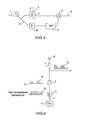
- the figure 2 shows an exemplary embodiment in the case where the control of the bias voltage 5 is performed by a photoconductive switch 6.
- the photoconductive switch 6 is, for example, made on a standard standard material AsGa or InP or the same type of material on which a AsGa deposition has been done at low temperature for example, or any other photoconductive material.
- the photoconductive switch 6 is optically activated by a pulsed laser source. From this pulsed laser source it receives optical pulse trains 21, each pulse having, for example, an average width of the order of some picoseconds.
- the photoconductive switch 6 activated by the optical pulses generates, from the power supply 7, a voltage for biasing the photodiode 4 charged or not on a load resistor 9, itself connected to a reference potential 22, for example , an electrical mass.
- the photodiode 4 detects or does not detect the microwave signal 1 present at its input and carried optically, for example, by the optical fiber 3.
- the signal present at the input is the carrier Optical modulated by the microwave signal 1.
- the signal 8 at the output of this photodiode 4 is, in this case, a series of pulses whose amplitude depends on the value of the microwave signal. These pulses of the output signal 8 have substantially the same width as the optical pulses which activate the polarization voltage generating device 6, they are modulated by the microwave signal 1.
- the input signal 1 is sampled at the frequency of the optical signal 21 which controls the bias voltage of the photodiode 4, with ultra-short sampling pulse widths.
- the photodiode 4 being an imperfect element, when it is not polarized, it lets pass a small part of signal whose level is nevertheless very weak. It is indeed at least 40 dB lower than when the photodiode is polarized.
- the figure 3 shows, by another embodiment, that it is possible by a technique identical to the neutrodynage to further reduce the minimum level at the output of the photodiode 4 when it is not polarized.
- a second photodiode 10 is used. This second photodiode is not polarized. This second photodiode 10 is also illuminated by the optical carrier of the microwave signal.
- another branch 31 of the optical fiber 3 is, for example, connected to this second photodiode 10.
- the optical fiber 3 on which the signal 1 to be converted is optically illuminated optically illuminates the two photodiodes 4, 10.
- the first photodiode 4 has its bias voltage controlled by the polarization generating device 6, whereas the second photodiode 10 does not have its bias voltage controlled.
- the signal at the output of the first photodiode 4 depends on its bias voltage and is therefore either representative of the microwave signal to be converted, or very low.
- the signal is very weak and identical to the output signal of the first photodiode 4 when it is not polarized.
- An adder 12 carries out the sum of the signal coming from the first photodiode 4 and the signal coming from the second photodiode 10 phase-shifted by 180 ° by a phase-shifter 11. In this embodiment, the output of the summator delivers the output signal 8 of the device according to the invention.
- the output signal of the adder 12 When the bias voltage of the first photodiode is zero, the output signal of the adder 12 is zero. Indeed, the low residual values of the outputs of the two photodiodes present at the input of the phase shifter vanish. The residual value present at the output of the first phase-shifter 4 thus disappears as well.
- the output signal 8 When the bias voltage of the photodiode 4 is not zero, the output signal 8 is representative of the signal to be converted. The small residual value of the second photodiode which is subtracted from this output signal 8 is then negligible.
- the figure 4 presents an exemplary embodiment, applied to the embodiment of the figure 2 , where the optical electrical converter 2 is made to using a pulsed laser source and an electro-optical modulator. There is actually a first sampling, in the optical domain, at the level of the converter 2 by means of the pulse source.
- the signal 41 present at the input of the photodiode is no longer the microwave signal 1 as in the case of the figure 2 , but a succession of pulses 42 whose amplitude is modulated by the microwave signal 1 that one seeks to convert.
- the pulses 21 which activate the device 6 for generating the bias voltage must be synchronized with the pulses 42 present at the input of the photodiode 4.
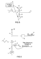
- the figure 5 shows another embodiment based on the use of a dual control and two photodiodes 4, 10 said balanced, the anode of the first photodiode 4 being connected to the cathode of the second photodiode 10.
- This embodiment allows to reduce the effects of the impulse control of the bias voltage of the photodiodes.
- the device of the figure 5 is based on the simultaneous control, by a laser source 14, of the two photodiodes 4, 10 biased by inverse voltages + V and -V by means of two devices 6, 13 of generations of bias voltages. In this system only a first photodiode 4 is illuminated by the optical carrier of the microwave signal 1 to be converted.
- the output 8 is connected to the middle point A of the two photodiodes 4, 10, located between the anode of the first photodiode 4 and the cathode of the second photodiode 10.
- the present signal is proportional to the signal to be converted but the effects due to the impulse control of the bias voltage are eliminated because they are subtracted at this point A because of the simultaneous control of the two photodiodes 4, 10 polarized by two opposite voltages.
- the output 8 has a substantially perfect zero.
- This embodiment presented by the figure 5 is another example allowing, as the embodiment of the figure 3 , to get a substantially perfect zero output.
- the figure 7 illustrates an example of the bandwidth of the filter 15. More precisely, it illustrates by a curve 71 the transfer function of this low-pass filter. The latter allows in particular to pass the sampling frequency f 0 which is included in its bandwidth. It filters in particular the frequency band 72 between two frequencies f 1 and f 2 , this band comprising the frequency of the signals 1 to be sampled present at the input of the device.
- the figure 8 illustrates the impulse response of the low-pass filter 15. This response is illustrated by a curve 81 representing a pulse as a function of time t.
- the time Th corresponds to the time for which the signal remains constant at the best of 1 ⁇ 2 LSB. This time is greater than or equal to the time required to perform an analog-to-digital conversion.
- An embodiment of the type of the figure 6 applies, for example, to convert a frequency signal between the frequencies f 1 and f 2 by means of a device made by interleaving several analog-to-digital converters operating at a sampling frequency f 0 , f 0 being less than f 1 .
- the figure 9 presents another example of embodiment.
- a device based on balanced photodiodes it is possible to use a device based on balanced photodiodes to increase the contrast and to overcome the effects of controlling the pulse bias voltage.
- the two photodiodes 4, 10 are illuminated by the optical fiber 3 carrying the signal 1 to be sampled, as in the embodiment of FIG. figure 3 .
- the polarization of the two photodiodes is always present via two resistors 9, 18, but only the first photodiode 4 is pulse-controlled.
- a resistor 9 connects the cathode of the first photodiode 4 to the potential + V.
- a resistor 18 connects the anode of the second photodiode 10 to the potential -V.
- the low-pass filter 15 is connected to the point A medium of two photodiodes 4, 10.
- the low-pass filter has the same characteristics as the previous one, illustrated in particular by the Figures 7 and 8 .
- a polarization control device 6 of the first photodiode connects its cathode to the reference potential 22. This control device 6 is always activated by the optical pulse train 21. The polarization of the two photodiodes is therefore always present, so that the signal 8 at the output of the filter 15 is always zero.
- the polarization control device 6 of the first photodiode 4 cancels the polarization of the first photodiode 4, a pulse is present at the output of the low-pass filter 15.
- the signal 8 at the output of the filter 15 comprises pulses whose amplitude depends on the value of the signal to be converted.
Landscapes
- Engineering & Computer Science (AREA)
- Theoretical Computer Science (AREA)
- Optical Communication System (AREA)
- Optical Modulation, Optical Deflection, Nonlinear Optics, Optical Demodulation, Optical Logic Elements (AREA)
Claims (14)
- Vorrichtung zur Abtastung eines Signals, die mindestens aufweist:- einen elektrisch-optischen Wandler (2), der eine vom Signal (1) modulierte optische Trägerwelle liefert;- einen optisch-elektrischen Wandler (4), der von der optischen Trägerwelle beleuchtet und von Spannungsimpulsen (5) gesteuert wird, wobei der optisch-elektrische Wandler (4) am Ausgang ein Signal (8) proportional zum Modulationssignal der optischen Trägerwelle liefert, wenn er spannungsgesteuert wird, wobei das Ausgangssignal (8) das abgetastete Signal ist;dadurch gekennzeichnet, dass der optisch-elektrische Wandler eine Photodiode (4) ist, deren Polarisation von den Spannungsimpulsen (5) gesteuert wird.
- Vorrichtung nach Anspruch 1, dadurch gekennzeichnet, dass der optisch-elektrische Wandler (4) am Ausgang ein Signal (8) proportional zum Modulationssignal der optischen Trägerwelle liefert, wenn die Spannung (5) ungleich Null ist.
- Vorrichtung nach einem der vorhergehenden Ansprüche, dadurch gekennzeichnet, dass die Spannungsimpulse (5) ausgehend von einer geschalteten Speisespannung (7) erzeugt werden, wobei die Spannung (7) von einem photoleitenden Schalter (6) geschaltet wird, wobei der photoleitende Schalter (6) von optischen Impulsen (21) aktiviert wird.
- Vorrichtung nach einem der vorhergehenden Ansprüche, dadurch gekennzeichnet, dass sie eine zweite Photodiode (10) aufweist, die von der optischen Trägerwelle beleuchtet wird, wobei die zweite Photodiode (10) nicht polarisiert ist und ihr Ausgangssignal vom Ausgangssignal der ersten Photodiode (4) subtrahiert wird, um das abgetastete Ausgangssignal (8) zu bilden.
- Vorrichtung nach Anspruch 4, dadurch gekennzeichnet, dass der Ausgang des zweiten Photodetektors (10) mit einem 180°-Phasenschieber (11) verbunden ist, wobei der Ausgang des ersten Photodetektors (4) und der Ausgang des Phasenschiebers (11) mit den Eingängen eines Summierglieds (12) verbunden sind, dessen Ausgang das abgetastete Ausgangssignal (8) liefert.
- Vorrichtung nach einem der vorhergehenden Ansprüche, dadurch gekennzeichnet, dass sie eine zweite Photodiode (10) aufweist, die nicht von der optischen Trägerwelle beleuchtet wird, wobei die Kathode der zweiten Photodiode (10) mit der Anode der ersten Photodiode (4) verbunden ist, wobei die zwei Photodioden gleichzeitig spannungsgesteuert werden, wobei das abgetastete Ausgangssignal (8) sich im Mittelpunkt (A) der zwei Photodioden befindet.
- Vorrichtung nach einem der vorhergehenden Ansprüche, dadurch gekennzeichnet, dass die Polarisationsspannung an die Photodiode (4) über einen Widerstand (16) angelegt wird, wobei die Polarisationsspannung von einem impulsgesteuerten Schalter (6) auf Null gesetzt wird, wobei ein Tiefpassfilter (15) das Signal am Ausgang der Photodiode (4) filtert, wobei der Ausgang des Filters das abgetastete Ausgangssignal (8) liefert.
- Vorrichtung nach Anspruch 7, dadurch gekennzeichnet, dass der impulsgesteuerte Schalter ein optisch gesteuerter Schalter (6) ist, der den Widerstand auf ein Bezugspotential (22) bringt, wenn er einen optischen Impuls (21) empfängt.
- Vorrichtung nach Anspruch 8, dadurch gekennzeichnet, dass die Anode der Photodiode (4) mit dem Widerstand (16) und mit dem optisch gesteuerten Schalter (6) verbunden ist, wobei der Widerstand (16) außerdem mit einer Speisespannung (7) verbunden ist, wobei der Schalter (6) von optischen Impulsen (21) aktiviert wird.
- Vorrichtung nach einem der vorhergehenden Ansprüche, dadurch gekennzeichnet, dass sie eine zweite Photodiode (10) aufweist, die von der optischen Trägerwelle beleuchtet wird, wobei die Kathode der zweiten Photodiode mit der Anode der ersten Photodiode (4) verbunden ist, wobei die zwei Photodioden gleichzeitig spannungsgesteuert werden, wobei die Polarisationsspannung der ersten Photodiode (4) impulsgesteuert wird, wobei ein Tiefpassfilter (15) mit dem Mittelpunkt (A) der zwei Photodioden verbunden ist, wobei der Ausgang des Tiefpassfilters (15) das abgetastete Ausgangssignal liefert.
- Vorrichtung nach Anspruch 10, dadurch gekennzeichnet, dass die erste Photodiode (4) mit einer Speisespannung +V über einen Widerstand (9) verbunden ist, die zweite Photodiode (10) mit einer Speisespannung -V über einen Widerstand (18) verbunden ist, wobei die Kathode der ersten Photodiode (4) von einem impulsgesteuerten Schalter (6) auf Null gesetzt wird.
- Vorrichtung nach einem der vorhergehenden Ansprüche, dadurch gekennzeichnet, dass die optische Trägerwelle im optischen Bereich abgetastet wird.
- Vorrichtung nach Anspruch 12, dadurch gekennzeichnet, dass der elektro-optische Wandler (2) eine Impulslaserquelle aufweist, die mit einem elektro-optischen Modulator gekoppelt ist.
- Vorrichtung nach einem der vorhergehenden Ansprüche, dadurch gekennzeichnet, dass die optische Trägerwelle von einer Lichtleitfaser (3, 31) transportiert wird.
Applications Claiming Priority (1)
| Application Number | Priority Date | Filing Date | Title |
|---|---|---|---|
| FR0413342A FR2879372B1 (fr) | 2004-12-15 | 2004-12-15 | Dispositif d'echantillonnage hautes frequences |
Publications (2)
| Publication Number | Publication Date |
|---|---|
| EP1672802A1 EP1672802A1 (de) | 2006-06-21 |
| EP1672802B1 true EP1672802B1 (de) | 2008-04-30 |
Family
ID=34954458
Family Applications (1)
| Application Number | Title | Priority Date | Filing Date |
|---|---|---|---|
| EP20050112069 Expired - Lifetime EP1672802B1 (de) | 2004-12-15 | 2005-12-13 | Hochgeschwindigkeitsabtastgerät |
Country Status (3)
| Country | Link |
|---|---|
| EP (1) | EP1672802B1 (de) |
| DE (1) | DE602005006369T2 (de) |
| FR (1) | FR2879372B1 (de) |
Families Citing this family (1)
| Publication number | Priority date | Publication date | Assignee | Title |
|---|---|---|---|---|
| CN108039540B (zh) * | 2017-12-04 | 2020-02-18 | 苏州六幺四信息科技有限责任公司 | 基于光电探测器的微波信号通断控制方法及光控微波开关 |
Family Cites Families (2)
| Publication number | Priority date | Publication date | Assignee | Title |
|---|---|---|---|---|
| JP2000147021A (ja) * | 1998-11-11 | 2000-05-26 | Ando Electric Co Ltd | 電気光学サンプリングオシロスコープ用受光回路 |
| FR2833780B1 (fr) * | 2001-12-18 | 2005-09-09 | Thales Sa | Dispositif de generation d'impulsions a fort taux d'extinction et systeme d'echantillonnage notamment de signaux hyperfrequence |
-
2004
- 2004-12-15 FR FR0413342A patent/FR2879372B1/fr not_active Expired - Fee Related
-
2005
- 2005-12-13 DE DE200560006369 patent/DE602005006369T2/de not_active Expired - Lifetime
- 2005-12-13 EP EP20050112069 patent/EP1672802B1/de not_active Expired - Lifetime
Also Published As
| Publication number | Publication date |
|---|---|
| FR2879372A1 (fr) | 2006-06-16 |
| DE602005006369D1 (de) | 2008-06-12 |
| EP1672802A1 (de) | 2006-06-21 |
| DE602005006369T2 (de) | 2009-06-18 |
| FR2879372B1 (fr) | 2007-06-01 |
Similar Documents
| Publication | Publication Date | Title |
|---|---|---|
| EP0975107B1 (de) | Sendevorrichtung für optische Daten | |
| FR2521369A1 (fr) | Circuit amplificateur comportant une annulation de la tension de decalage | |
| CA2220603C (fr) | Dispositif d'emission de donnees optiques | |
| FR2750552A1 (fr) | Recepteur pour systeme de transmission de signaux numeriques par voie optique | |
| EP0004815B1 (de) | Verfahren zum Übertragen elektrischer Signale mittels optischer Verbindung und Vorrichtung zur automatischen Verstärkungsregelung eines an der optischen Verbindung gekuppelten Empfangsweges | |
| EP0632310A1 (de) | Vorrichtung zur Vorspannungssteuerung einer optischen Quelle | |
| EP0859268A1 (de) | Wellenlängenwandler für binären optischen signalen | |
| FR2523782A1 (fr) | Circuit amplificateur a transistor a effet de champ | |
| FR2651389A1 (fr) | Amplificateur differentiel a couplage capacitif. | |
| FR2922388A1 (fr) | Quantificateur, convertisseur analogique-numerique comprenant un tel quantificateur, et recepteur ultra-large bande integrant un tel convertisseur | |
| WO1992010780A1 (fr) | Dispositif de modulation electrooptique integre | |
| EP0667677A1 (de) | Anordnung zur Multiplizierung einer Kapazität mit einem variierbarem Koeffizienten zur Grenzfrequenzregulung eines Filters und Filter mit einer derartigen Anordnung | |
| EP3053274B1 (de) | Zeitkontinuierliche quantisierungsvorrichtung, funkfrequenzsignalempfänger mit einer derartigen vorrichtung und zeitkontinuierliches quantisierungsverfahren | |
| EP1672802B1 (de) | Hochgeschwindigkeitsabtastgerät | |
| EP0915540B1 (de) | Integrierte lichtemittierende Vorrichtung, die mindestens einen Laserabschnitt und einen Modulatorabschnitt enthält | |
| FR2588433A1 (fr) | Filtre a fonction de transfert commutable et boucle a verrouillage de phase incluant ledit filtre | |
| WO2007057394A1 (fr) | Dispositif de mesure de profil d'impulsions monocoup de tres courte duree | |
| EP1499042B1 (de) | Differentieller Kodierer für elektrische Signale | |
| WO2008113675A1 (fr) | Echantillonneur-bloqueur protege contre des parasites de commutation | |
| FR2472880A1 (fr) | Dispositif de controle automatique de gain a action optique dans un systeme de transmission de signaux electriques par liaison optique | |
| EP1296446A1 (de) | Gegentakt-Mischer unter Verwendung von bipolaren Transistoren | |
| FR3061783B1 (fr) | Modulateur optique dote de diodes mach-zender de longueur reduite | |
| CA2338873A1 (fr) | Dispositif d'amplification optique | |
| EP1324056B1 (de) | Optischer Impulsgeber mit hoher Extinktionsrate und Abtastsystem insbesondere für Mikrowellensignale | |
| FR2702053A1 (fr) | Dispositif à grande linéarité de limitation d'une caractéristique d'un signal, et utilisation du dispositif dans une chaîne de réception radar. |
Legal Events
| Date | Code | Title | Description |
|---|---|---|---|
| PUAI | Public reference made under article 153(3) epc to a published international application that has entered the european phase |
Free format text: ORIGINAL CODE: 0009012 |
|
| AK | Designated contracting states |
Kind code of ref document: A1 Designated state(s): AT BE BG CH CY CZ DE DK EE ES FI FR GB GR HU IE IS IT LI LT LU LV MC NL PL PT RO SE SI SK TR |
|
| AX | Request for extension of the european patent |
Extension state: AL BA HR MK YU |
|
| 17P | Request for examination filed |
Effective date: 20061215 |
|
| 17Q | First examination report despatched |
Effective date: 20070116 |
|
| AKX | Designation fees paid |
Designated state(s): DE GB IT SE |
|
| GRAP | Despatch of communication of intention to grant a patent |
Free format text: ORIGINAL CODE: EPIDOSNIGR1 |
|
| GRAS | Grant fee paid |
Free format text: ORIGINAL CODE: EPIDOSNIGR3 |
|
| GRAA | (expected) grant |
Free format text: ORIGINAL CODE: 0009210 |
|
| AK | Designated contracting states |
Kind code of ref document: B1 Designated state(s): DE GB IT SE |
|
| REG | Reference to a national code |
Ref country code: GB Ref legal event code: FG4D Free format text: NOT ENGLISH |
|
| REF | Corresponds to: |
Ref document number: 602005006369 Country of ref document: DE Date of ref document: 20080612 Kind code of ref document: P |
|
| REG | Reference to a national code |
Ref country code: SE Ref legal event code: TRGR |
|
| PLBE | No opposition filed within time limit |
Free format text: ORIGINAL CODE: 0009261 |
|
| STAA | Information on the status of an ep patent application or granted ep patent |
Free format text: STATUS: NO OPPOSITION FILED WITHIN TIME LIMIT |
|
| 26N | No opposition filed |
Effective date: 20090202 |
|
| PGFP | Annual fee paid to national office [announced via postgrant information from national office to epo] |
Ref country code: DE Payment date: 20101208 Year of fee payment: 6 |
|
| PGFP | Annual fee paid to national office [announced via postgrant information from national office to epo] |
Ref country code: SE Payment date: 20111213 Year of fee payment: 7 |
|
| PG25 | Lapsed in a contracting state [announced via postgrant information from national office to epo] |
Ref country code: SE Free format text: LAPSE BECAUSE OF NON-PAYMENT OF DUE FEES Effective date: 20121214 |
|
| REG | Reference to a national code |
Ref country code: DE Ref legal event code: R119 Ref document number: 602005006369 Country of ref document: DE Effective date: 20130702 |
|
| PG25 | Lapsed in a contracting state [announced via postgrant information from national office to epo] |
Ref country code: DE Free format text: LAPSE BECAUSE OF NON-PAYMENT OF DUE FEES Effective date: 20130702 |
|
| PGFP | Annual fee paid to national office [announced via postgrant information from national office to epo] |
Ref country code: GB Payment date: 20131211 Year of fee payment: 9 |
|
| PGFP | Annual fee paid to national office [announced via postgrant information from national office to epo] |
Ref country code: IT Payment date: 20131213 Year of fee payment: 9 |
|
| GBPC | Gb: european patent ceased through non-payment of renewal fee |
Effective date: 20141213 |
|
| PG25 | Lapsed in a contracting state [announced via postgrant information from national office to epo] |
Ref country code: GB Free format text: LAPSE BECAUSE OF NON-PAYMENT OF DUE FEES Effective date: 20141213 |
|
| PG25 | Lapsed in a contracting state [announced via postgrant information from national office to epo] |
Ref country code: IT Free format text: LAPSE BECAUSE OF NON-PAYMENT OF DUE FEES Effective date: 20141213 |