EP1499042B1 - Differentieller Kodierer für elektrische Signale - Google Patents
Differentieller Kodierer für elektrische Signale Download PDFInfo
- Publication number
- EP1499042B1 EP1499042B1 EP04291590A EP04291590A EP1499042B1 EP 1499042 B1 EP1499042 B1 EP 1499042B1 EP 04291590 A EP04291590 A EP 04291590A EP 04291590 A EP04291590 A EP 04291590A EP 1499042 B1 EP1499042 B1 EP 1499042B1
- Authority
- EP
- European Patent Office
- Prior art keywords
- signal
- master
- control signal
- bistable
- coder
- Prior art date
- Legal status (The legal status is an assumption and is not a legal conclusion. Google has not performed a legal analysis and makes no representation as to the accuracy of the status listed.)
- Expired - Lifetime
Links
- 230000000295 complement effect Effects 0.000 claims description 18
- 230000003321 amplification Effects 0.000 claims description 7
- 230000005540 biological transmission Effects 0.000 claims description 7
- 238000003199 nucleic acid amplification method Methods 0.000 claims description 7
- 230000001360 synchronised effect Effects 0.000 claims description 4
- 230000001960 triggered effect Effects 0.000 claims description 4
- 230000010363 phase shift Effects 0.000 claims description 2
- 235000021183 entrée Nutrition 0.000 description 12
- 230000006978 adaptation Effects 0.000 description 4
- 230000003287 optical effect Effects 0.000 description 4
- 238000005516 engineering process Methods 0.000 description 2
- 230000010354 integration Effects 0.000 description 2
- 238000007493 shaping process Methods 0.000 description 2
- 239000006185 dispersion Substances 0.000 description 1
- 230000010287 polarization Effects 0.000 description 1
- 230000003595 spectral effect Effects 0.000 description 1
- 230000007704 transition Effects 0.000 description 1
Images

Classifications
-
- H—ELECTRICITY
- H04—ELECTRIC COMMUNICATION TECHNIQUE
- H04L—TRANSMISSION OF DIGITAL INFORMATION, e.g. TELEGRAPHIC COMMUNICATION
- H04L25/00—Baseband systems
- H04L25/38—Synchronous or start-stop systems, e.g. for Baudot code
- H04L25/40—Transmitting circuits; Receiving circuits
- H04L25/49—Transmitting circuits; Receiving circuits using code conversion at the transmitter; using predistortion; using insertion of idle bits for obtaining a desired frequency spectrum; using three or more amplitude levels ; Baseband coding techniques specific to data transmission systems
-
- H—ELECTRICITY
- H04—ELECTRIC COMMUNICATION TECHNIQUE
- H04L—TRANSMISSION OF DIGITAL INFORMATION, e.g. TELEGRAPHIC COMMUNICATION
- H04L25/00—Baseband systems
- H04L25/38—Synchronous or start-stop systems, e.g. for Baudot code
- H04L25/40—Transmitting circuits; Receiving circuits
- H04L25/49—Transmitting circuits; Receiving circuits using code conversion at the transmitter; using predistortion; using insertion of idle bits for obtaining a desired frequency spectrum; using three or more amplitude levels ; Baseband coding techniques specific to data transmission systems
- H04L25/497—Transmitting circuits; Receiving circuits using code conversion at the transmitter; using predistortion; using insertion of idle bits for obtaining a desired frequency spectrum; using three or more amplitude levels ; Baseband coding techniques specific to data transmission systems by correlative coding, e.g. partial response coding or echo modulation coding transmitters and receivers for partial response systems
Definitions
- the present invention relates to the field of electronics applied in particular to optical telecommunications and more specifically relates to a differential encoder of electrical signals.
- a precoded electrical data signal is constructed beforehand.
- pp884-886 proposes a precoder operating at a rate of 10 Gbit / s.
- This precoder mainly comprises two discrete modules: a conventional AND logic gate and a Toggle Flip Flop (T-FF).
- the AND logic gate receives a 10 GHz sinusoidal clock signal and an input data signal at the same bit rate and in the form of a data sequence corresponding to the binary value '0' or the value binary '1', in non-return to zero (NRZ) format.
- This logic AND gate outputs a signal for controlling the flip-flop T and similar to the clock signal when the input bit data corresponds to '1' and remains constant when the binary data corresponds to '0'.
- the flip-flop T changes state when the control signal corresponds to a clock signal, that is to say when the input data corresponds to the binary data '1'.
- the flip-flop T does not change state when the control signal is constant, that is to say when the input data corresponds to the binary data '0'.
- the AND logic gate has a bandwidth limited by its technology. At high frequency, ie above 10 GHz, this gate may produce a distorted control signal that is to say amplitude too small to be detected by the flip-flop T and / or with rise times and descent insufficiently steep. Also, data may be lost and the precoded signal may be of poor quality.
- the logic gate assumes accurate alignment of the clock and the input data signal.
- the invention aims to provide a differential encoder of electrical signals capable of providing a binary signal of good quality data, even at high speed while being simple design.
- the differential encoder according to the invention is integrated in the sense that the control means and the latch T are brought together in one and the same circuit and are optimized relative to each other.
- this integration makes it possible to differentiate the control of the master flip-flop and the control of the slave flip-flop.
- the slave latch receives a clean and regular slave control signal, that is to say, freed from the noise of commutations, and of sufficient amplitude. This ensures an output data signal without time jitter and having sharp transitions.
- the master control signal is substantially in phase with the clock signal and is substantially in phase opposition with the slave control signal.
- Such a circuit is simple architecture and more robust, can thus operate at high speed.
- the control means according to the invention tolerate a wider phase margin between the input data signal and the clock signal.
- integration has the advantage of reducing power consumption.
- the duration of the level change can be equal to or advantageously less than the bit time, whereas with an AND gate it is strictly equal to a bit time.
- this level change time is chosen substantially equal to half a bit time.
- the first circuit may be capable of supplying a so-called subsidiary master control signal which is selected complementary to said master or constant control signal and injected into a subsidiary control input of the master flip-flop.
- the second circuit may be able to provide a so-called subsidiary slave control signal which is selected complementary to said slave or constant control signal and injected into a subsidiary control input of the slave latch.
- the first circuit comprises an analog comparator of the input data signal and the clock signal which is capable of supplying at least said master control signal.
- the analog comparator may comprise a differential pair provided with two transistors respectively voltage-controlled by the clock signal and the input data signal and is capable of supplying a complementary subsidiary master control signal complementary to said signal.
- master and is fed into a subsidiary control input of the master flip-flop.
- said second value is selected within the range of values of the clock signal.
- the first circuit may comprise a signal amplification stage, downstream of the analog comparator, and of structure similar to the structure of the analog comparator.
- the differential encoder according to the invention can be made based on heterojunction bipolar transistors, especially fast transistors.
- the invention also applies to an encoder chosen from the duobinary coders, the phase-phase binary transmission coders controlled, and the differential phase modulation encoders and including a precoder corresponding to the differential encoder as defined above.
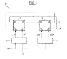
- FIG. 1 shows an integrated electrical signal differential encoder 10 comprising a flip-flop T formed of a master flip-flop 11 and a slave flip-flop 12 and a control circuit formed by a first circuit 21 and a second circuit. circuit 22.
- the main local input D1 of the master flip-flop 11 is connected with the subsidiary output S2 'of the slave flip-flop 12 while the subsidiary local input D1' of the master flip-flop 11 is connected with the main output S2 of the slave flip-flop 12
- the main and subsidiary outputs of the master flip-flop 11 are respectively connected to the main and subsidiary inputs of the slave flip-flop 12.
- the crossing is done between the outputs S1, S'1 of the master flip-flop 11 and the inputs D2, D2 'of the slave flip-flop 12.
- the main and subsidiary outputs S2, S2 'of the slave latch 12 respectively deliver an output data signal S and its complement S *, precoded signals that can be used to form a duobinary signal, a PSBT signal or a DPSK signal.
- the first circuit 21 dedicated to the master flip-flop 11 receives a clock signal CK and a data input signal DATA substantially synchronized with the clock signal.
- This first circuit 21 outputs a control signal called master A which is injected into the main control input E1 and a control signal said subsidiary master A * complementary to said first master control signal A and which is injected into the subsidiary command entry E1 '.
- the circuit 21 is such that it delivers a subsidiary master signal A * constant.
- the second circuit 22, dedicated to the slave latch 12, receives the clock signal CK and supplies a so-called slave control signal CK2 which is injected into the main control input E2 and which is representative of the complement of the clock signal and a so-called subsidiary slave control signal CK2 * which is representative, for example, similar to the clock signal and is fed into the subsidiary control input E2 '.
- the circuit 22 is such that it delivers a subsidiary slave control signal CK2 * constant.
- the slave control signal CK2 for example a sinusoid and is substantially in phase opposition with the master control signal A when the latter changes level.
- the subsidiary slave control signal CK2 * is substantially in phase with the subsidiary master control signal A * when the latter changes level.
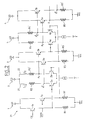
- FIG. 2 details a preferred example of structure of the first circuit 21 and with FIGS. 3a to 3c which are chronograms of the characteristic signals CK, DATA, A, A *, S, S *.
- Each matching stage 1, 3, 5 respectively is produced from transistors, for example bipolar heterojunction identical 1 to 1b, 3a to 3b, 5a to 5b respectively coupled to identical resistors R1 to R1 ', R3 to R3' , R5 to R5 'respectively to form tracking emitters.
- each of the resistors R1 to R5 ' is approximately 100 ohms.
- the collectors of transistors 1a to 1b, 3a to 3b, 5a to 5b are connected to a stable potential GND and the resistors R1 to R5 'to another stable potential Vcc.
- the analog comparator 2 comprises a first and a second bipolar transistors 2a, 2b mounted as a common emitter thus forming a differential pair, and connected to a current source 1, for example 35 mA.
- the collectors are connected to first and second identical load resistors R2, R2 'respectively, for example equal to 25 Ohms about. These load resistors R2, R2 'are also connected to a stable voltage GND serves to bias this differential pair.
- the signal amplification and shaping stage 4 comprises two bipolar transistors 4a, 4b mounted as a common emitter and connected to a current source, for example 25 mA, forming a second differential pair.
- the collectors are connected to identical load resistors R4, R4 'respectively, for example equal to approximately 25 Ohms. These load resistors R4, R4 'are also connected to a stable voltage GND serves to bias this second differential pair.
- the clock signal CK is a voltage, for example in sinusoidal form, for example between -800 mV and -200 mV, of average level MOY for example equal to about -500 mV, of period T 0 , for example 25 ps corresponding to a frequency of 40 GHz.
- a data input signal DATA is chosen which is a voltage, for example impulse and in the form of slots, of bit time T bit equal to the clock period T 0 and preferably relatively synchronized with the signal of CK clock.
- This data signal DATA has a first level N1 greater than the values taken by the clock signal and for example equal to approximately 0 mV and a second level N2 between the minimum and maximum value taken by the clock signal CK and preferably equal to the average level MOY for an optimal setting.
- the clock signal CK after passing through one of the transistors of the first matching circuit 1a drives the base of the first transistor 2a of the comparator 2.
- the input data signal DATA after passing through the other one of the transistors of the first matching circuit 1b drives the base of the second transistor 2b of the comparator 2.
- these signals CK, DATA control in voltage the first differential pair.
- the input data signal DATA defines a data sequence in a non-return format to zero: the first level N1 corresponding for example to a data or logical state '0' and the second level N2 corresponding for example to a data or logical state '1'.
- the sequence illustrated in FIG. 3a is then the following: 0100101110100101100100010.
- I 2 the current flowing in a first branch 21 including the first load resistor R2 and the first transistor 2a and I2 'of the comparator 2 and I' 2 the current flowing in a second branch 22 including the second resistor. charge R2 'and the second transistor 2b of comparator 2.
- intermediate output voltage A 1 the output voltage of the comparator 2 located at the collector of the second transistor 2b of the comparator 2.
- complementary intermediate output voltage A * 1 the complementary output voltage to A 1 and located at the collector of the first transistor 2a of the comparator 2.
- the current I 2 is then substantially equal to I while the current I 2 is very low: the intermediate output voltage A 1 (respectively A * 1 ) is forced (stabilized) to its minimum level (respectively maximum).
- the intermediate output voltage A 1 will go from a very low minimum value to a maximum value and then return to the minimum value thus forming a peak width at half height substantially equal to half a bit time.
- the complementary intermediate output voltage A * 1 will go from a maximum value to a minimum value and then return to the maximum value thus forming a valley.
- the intermediate output voltage A 1 after passing through one of the transistors 3b of the second matching circuit 3 drives the base of the first transistor 4a of the amplification stage 4.
- the complementary intermediate output voltage A * 1 after passing through the other of the transistors 3a of the second matching circuit 3 drives the base of the second transistor 4b of the amplifier stage 4.
- the second differential pair supplies, at the output, so-called final output voltages A 2 , A * 2, amplified and shaped and reproducing the profile of the peaks and valleys of the intermediate output voltages A 1 , A * 1 .
- the first circuit 21 does not include a second amplification stage nor adaptation stages 3 and 5: the signals A 1 and A * 1 then being the control signals of the master flip-flop.
- the master control signal A is thus defined by a stable minimum level ST for example at -500 mV, and by a level or peak change P 1 to P 11 of width at half height t 1 substantially equal to half a bit time and for example a maximum value equal to 0 mV.
- the complementary control signal A is defined by a stable maximum level ST 'and by a level change or valley VAL of width at half height substantially equal to half a bit time.
- each peak P 1 to P 11 triggers (see arrow F) a change of state associated with a switching of levels C 1 to C 10 of the data binary output signal S.
- Each switching C 1 to C 10 is less than or equal to a bit time and lasts for example one third of bit time.
- the level change can be made closer to the least noisy level.
- the binary output signal S is in a stabilized binary state, for example two successive '0' over two bit time slots.
- the binary output signal S changes state, for example from '0' to '1'.
- the output data signal S has a low level Na for example at about -500 mV and a high level Nb for example at about 0 mV.
- each VAL valley triggers a change of state associated with a switching of the complementary binary data output signal S *.
Landscapes
- Physics & Mathematics (AREA)
- Spectroscopy & Molecular Physics (AREA)
- Engineering & Computer Science (AREA)
- Computer Networks & Wireless Communication (AREA)
- Signal Processing (AREA)
- Manipulation Of Pulses (AREA)
- Analogue/Digital Conversion (AREA)
- Transmission And Conversion Of Sensor Element Output (AREA)
- Logic Circuits (AREA)
Claims (8)
- Differentieller Kodierer (10) für elektrische Signale, beinhaltend- Steuerungsmittel (21, 22),- die geeignet sind, ein Clocksignal (CK), das eine Bitdauer definiert, und ein mit dem Clocksignal synchronisiertes binäres Eingangsdatensignal (DATA) zu empfangen, wobei das Eingangsdatensignal eine Sequenz von ersten und zweiten Werten (N1, N2) in einem Non-Return-to-Zero-Format definiert,- und die geeignet sind, ein Steuersignal (A) zu liefern, das durch einen als stabil bezeichneten Pegel (ST) und eine Pegeländerung (von P1 auf P11) definiert ist, die ausgelöst wird, wenn das Eingangsdatensignal dem zweiten Wert entspricht,- ein T-Flipflop, das von den Steuerungsmitteln angesteuert wird und geeignet ist, ein binäres Ausgangsdatensignal (S, S*) mit einem Low-Pegel (Na) und einem High-Pegel (Nb) zu liefern, das definiert ist durchdadurch gekennzeichnet, daß das T-Flipflop ein Master-Flipflop (11), gefolgt von einem Slave-Flipflop (12), beinhaltet, die jeweils einen Hauptsteuereingang (E1, E2) beinhalten,- einen über zwei aufeinanderfolgende Bitdauerintervalle identischen Binärzustand ('0', '1'), und, wenn das Steuersignal auf dem stabilen Pegel verbleibt,- eine Pegeländerung, die einer Umschaltung (von C1 auf C10) eines der Low- und High-Pegel auf den jeweils anderen High- und Low-Pegel zugeordnet ist und durch besagte Pegeländerung ausgelöst wird,
sowie dadurch, daß der differentielle Kodierer integriert ist und besagte Steuerungsmittel- eine erste Schaltung (21), die dem Master-Flipflop zugewiesen und dafür ausgelegt ist, besagtes als Master-Signal bezeichnetes Steuersignal (A) zu liefern, das dem Hauptsteuereingang des Master-Flipflops zugeführt wird, sowie- eine zweite Schaltung (22), die dem Slave-Flipflop zugewiesen ist, von besagtem Clocksignal (CK) gesteuert wird und dafür ausgelegt ist, ein als Slave-Signal (CK2) bezeichnetes Steuersignal zu liefern, das ein zum Clocksignal komplementäres Signal bildet und dem Hauptsteuereingang des Slave-Flipflops zugeführt wird, beinhalten. - Differentieller Kodierer (10) für elektrische Signale gemäß Anspruch 1, dadurch gekennzeichnet, daß die Zeitspanne der Pegeländerung kleiner als oder ebenso groß wie die Bitdauer und vorzugsweise gleich der halben Bitdauer ist.
- Differentieller Kodierer (10) für elektrische Signale gemäß einem der Ansprüche 1 oder 2, dadurch gekennzeichnet, daß die erste Schaltung (21) geeignet ist, ein als Master-Zusatzsignal (A*) bezeichnetes Steuersignal zu liefern, das komplementär zu besagtem Master-Steuersignal oder konstant gewählt, und einem Zusatz-Steuereingang (E1') des Master-Flipflops zugeführt wird, sowie dadurch, daß die zweite Schaltung (22) geeignet ist, ein als Slave-Zusatzsignal bezeichnetes Steuersignal zu liefern, das komplementär zu besagtem Slave-Steuersignal (CK2*) oder konstant gewählt und einem Zusatz-Steuereingang (E2') des Slave-Flipflops zugeführt wird.
- Differentieller Kodierer (10) für elektrische Signale gemäß einem der Ansprüche 1 bis 3, dadurch gekennzeichnet, daß die erste Schaltung (21) einen analogen Komparator (2) für das Eingangsdatensignal (DATA) und das Clocksignal (CK) beinhaltet, der geeignet ist, zumindest besagtes Master-Steuersignal (A) zu liefern.
- Differentieller Kodierer (10) für elektrische Signale gemäß Anspruch 4, dadurch gekennzeichnete daß der analoge Komparator (2) ein differentielles Paar beinhaltet, das aus zwei Transistoren (2a, 2b) besteht, die vom Clocksignal (CK) beziehungsweise vom Eingangsdatensignal (DATA) spannungsgesteuert werden, und das geeignet ist, ein Steuersignal zu liefern, das als zum besagten Master-Steuersignal komplementäres Master-Zusatzsignal (A*) bezeichnet und einem Zusatz-Steuereingang (E1') des Master-Flipflops zugeführt wird, sowie dadurch, daß der besagte zweite Wert (N2) so gewählt wird, daß er im Wertebereich des Clocksignals (CK) liegt.
- Differentieller Kodierer (10) für elektrische Signale gemäß einem der Ansprüche 4 oder 5, dadurch gekennzeichnet, daß die erste Schaltung (21) eine Signalverstärkungsstufe (3) beinhaltet, die im Signalweg hinter dem analogen Komparator (2) liegt und in seiner Struktur der Struktur des analogen Komparators ähnelt.
- Differentieller Kodierer (10) für elektrische Signale gemäß einem der Ansprüche 1 bis 6, dadurch gekennzeichnet, daß dieser auf der Basis von Heteroübergangs-Bipolartransistoren (2a bis 4b) realisiert ist.
- Differentieller Kodierer (10) für elektrische Signale, ausgewählt aus Duobinär-Kodierern, binären Sendekodierern mit phasengeregeltem Profil und Phasendifferenz-Modulationskodierern und beinhaltend einen Vorkodierer entsprechend dem gemäß einem der Ansprüche 1 bis 7 definierten differentiellen Kodierer.
Applications Claiming Priority (2)
| Application Number | Priority Date | Filing Date | Title |
|---|---|---|---|
| FR0308769 | 2003-07-18 | ||
| FR0308769A FR2857800B1 (fr) | 2003-07-18 | 2003-07-18 | Codeur differentiel de signaux electriques |
Publications (2)
| Publication Number | Publication Date |
|---|---|
| EP1499042A1 EP1499042A1 (de) | 2005-01-19 |
| EP1499042B1 true EP1499042B1 (de) | 2006-08-16 |
Family
ID=33462557
Family Applications (1)
| Application Number | Title | Priority Date | Filing Date |
|---|---|---|---|
| EP04291590A Expired - Lifetime EP1499042B1 (de) | 2003-07-18 | 2004-06-23 | Differentieller Kodierer für elektrische Signale |
Country Status (5)
| Country | Link |
|---|---|
| US (1) | US7023256B2 (de) |
| EP (1) | EP1499042B1 (de) |
| AT (1) | ATE336834T1 (de) |
| DE (1) | DE602004001939T2 (de) |
| FR (1) | FR2857800B1 (de) |
Families Citing this family (3)
| Publication number | Priority date | Publication date | Assignee | Title |
|---|---|---|---|---|
| JP4675721B2 (ja) * | 2005-08-31 | 2011-04-27 | 三菱電機株式会社 | パラレルプリコーダ回路 |
| JP4597820B2 (ja) * | 2005-09-05 | 2010-12-15 | 三菱電機株式会社 | パラレルプリコーダ回路 |
| US8275257B2 (en) * | 2007-04-17 | 2012-09-25 | Cisco Technology, Inc. | Differential quadrature phase-shift keying transmission system with variable transmission rate |
Family Cites Families (6)
| Publication number | Priority date | Publication date | Assignee | Title |
|---|---|---|---|---|
| US5267269A (en) * | 1991-09-04 | 1993-11-30 | Level One Communications, Inc. | System and method employing predetermined waveforms for transmit equalization |
| SE522272C2 (sv) * | 1997-08-20 | 2004-01-27 | Ericsson Telefon Ab L M | Optiskt duobinärt sändarsystem och förfarande som använder optisk intensitetsmodulering |
| US6452433B1 (en) * | 2000-05-31 | 2002-09-17 | Conexant Systems, Inc. | High phase margin low power flip-flop |
| US6496297B1 (en) * | 2000-12-22 | 2002-12-17 | Ciena Corporation | Device and method for modulating an optical signal |
| US7068948B2 (en) * | 2001-06-13 | 2006-06-27 | Gazillion Bits, Inc. | Generation of optical signals with return-to-zero format |
| US6850104B2 (en) * | 2003-03-10 | 2005-02-01 | Texas Instruments Incorporated | Master-slave latch with transparent mode |
-
2003
- 2003-07-18 FR FR0308769A patent/FR2857800B1/fr not_active Expired - Fee Related
-
2004
- 2004-06-23 EP EP04291590A patent/EP1499042B1/de not_active Expired - Lifetime
- 2004-06-23 DE DE602004001939T patent/DE602004001939T2/de not_active Expired - Lifetime
- 2004-06-23 AT AT04291590T patent/ATE336834T1/de not_active IP Right Cessation
- 2004-07-16 US US10/892,281 patent/US7023256B2/en not_active Expired - Fee Related
Also Published As
| Publication number | Publication date |
|---|---|
| EP1499042A1 (de) | 2005-01-19 |
| US20050012534A1 (en) | 2005-01-20 |
| FR2857800B1 (fr) | 2005-09-23 |
| DE602004001939T2 (de) | 2007-10-04 |
| DE602004001939D1 (de) | 2006-09-28 |
| US7023256B2 (en) | 2006-04-04 |
| FR2857800A1 (fr) | 2005-01-21 |
| ATE336834T1 (de) | 2006-09-15 |
Similar Documents
| Publication | Publication Date | Title |
|---|---|---|
| EP0181664B1 (de) | Synchronisierter Komparator | |
| EP1085659B1 (de) | Digital-Analog-Wandler des Stromtyps | |
| EP1677422A1 (de) | Vorrichtung zur Umwandlung eines übertragenen Signals in ein digitales Signal | |
| FR2618621A1 (fr) | Circuits pour un convertisseur numerique-analogique cmos | |
| EP0029767A1 (de) | Steuerungsverfahren einer Darlingtonschaltung und Darlingtonschaltung mit geringen Verlusten | |
| FR2473810A1 (fr) | Procede de compensation de la tension de decalage d'un amplificateur differentiel et macro-fonctionnelle en resultant | |
| CH661394A5 (fr) | Circuit et procede pour detecter un mot de correlation numerique donne. | |
| EP1499042B1 (de) | Differentieller Kodierer für elektrische Signale | |
| EP1039643A1 (de) | Analog-Digital-Wandleranordnung mit konstanter differentieller nicht-linearität | |
| FR2495409A1 (fr) | Commutateur a valeur de seuil | |
| EP0932094B1 (de) | Vorrichtung zur Erzeugung rauscharmer Stromstösse | |
| EP0022015A1 (de) | Audioverstärker und Verfahren zur Audiofrequenzverstärkung | |
| FR2744304A1 (fr) | Convertisseur numerique-analogique differentiel a fonction de filtrage et compensation de decalage | |
| EP0203645B1 (de) | Integrierte Digital/Analog-Wandlerschaltung mit Gerät zur Glitchreduzierung | |
| EP1455451B1 (de) | Vorrichtung zur optischen Signalverarbeitung | |
| FR2477802A1 (fr) | Circuit d'amplification | |
| EP0556927B1 (de) | Differenzschaltung mit hoher Linearität | |
| FR2873245A1 (fr) | Procede de traitement en mode differentiel d'une tension incidente relativement a une tension de reference et dispositif correspondant | |
| WO2008113675A1 (fr) | Echantillonneur-bloqueur protege contre des parasites de commutation | |
| EP0130646B1 (de) | Synchronisierter Komparator | |
| EP0838901B1 (de) | Analog-Digital-Wandlungsgerät mit geregelter Eingangsdynamik | |
| EP0349028A2 (de) | Integrierte Halbleiterschaltung mit einem differentiellen Paar von FETs | |
| FR2800531A1 (fr) | Amplificateur de frequences radioelectriques ayant un modulateur de phase a double rampe | |
| EP1672802B1 (de) | Hochgeschwindigkeitsabtastgerät | |
| EP0404630B1 (de) | Vorrichtung zum Empfang von über zwei kapazitiv gekoppelte Leitungen durchgehenden Informationen, insbesondere für Kraftfahrzeuge |
Legal Events
| Date | Code | Title | Description |
|---|---|---|---|
| PUAI | Public reference made under article 153(3) epc to a published international application that has entered the european phase |
Free format text: ORIGINAL CODE: 0009012 |
|
| AK | Designated contracting states |
Kind code of ref document: A1 Designated state(s): AT BE BG CH CY CZ DE DK EE ES FI FR GB GR HU IE IT LI LU MC NL PL PT RO SE SI SK TR |
|
| AX | Request for extension of the european patent |
Extension state: AL HR LT LV MK |
|
| 17P | Request for examination filed |
Effective date: 20050719 |
|
| AKX | Designation fees paid |
Designated state(s): AT BE BG CH CY CZ DE DK EE ES FI FR GB GR HU IE IT LI LU MC NL PL PT RO SE SI SK TR |
|
| GRAP | Despatch of communication of intention to grant a patent |
Free format text: ORIGINAL CODE: EPIDOSNIGR1 |
|
| GRAC | Information related to communication of intention to grant a patent modified |
Free format text: ORIGINAL CODE: EPIDOSCIGR1 |
|
| GRAS | Grant fee paid |
Free format text: ORIGINAL CODE: EPIDOSNIGR3 |
|
| GRAA | (expected) grant |
Free format text: ORIGINAL CODE: 0009210 |
|
| AK | Designated contracting states |
Kind code of ref document: B1 Designated state(s): AT BE BG CH CY CZ DE DK EE ES FI FR GB GR HU IE IT LI LU MC NL PL PT RO SE SI SK TR |
|
| PG25 | Lapsed in a contracting state [announced via postgrant information from national office to epo] |
Ref country code: AT Free format text: LAPSE BECAUSE OF FAILURE TO SUBMIT A TRANSLATION OF THE DESCRIPTION OR TO PAY THE FEE WITHIN THE PRESCRIBED TIME-LIMIT Effective date: 20060816 Ref country code: SK Free format text: LAPSE BECAUSE OF FAILURE TO SUBMIT A TRANSLATION OF THE DESCRIPTION OR TO PAY THE FEE WITHIN THE PRESCRIBED TIME-LIMIT Effective date: 20060816 Ref country code: IT Free format text: LAPSE BECAUSE OF FAILURE TO SUBMIT A TRANSLATION OF THE DESCRIPTION OR TO PAY THE FEE WITHIN THE PRESCRIBED TIME-LIMIT;WARNING: LAPSES OF ITALIAN PATENTS WITH EFFECTIVE DATE BEFORE 2007 MAY HAVE OCCURRED AT ANY TIME BEFORE 2007. THE CORRECT EFFECTIVE DATE MAY BE DIFFERENT FROM THE ONE RECORDED. Effective date: 20060816 Ref country code: NL Free format text: LAPSE BECAUSE OF FAILURE TO SUBMIT A TRANSLATION OF THE DESCRIPTION OR TO PAY THE FEE WITHIN THE PRESCRIBED TIME-LIMIT Effective date: 20060816 Ref country code: PL Free format text: LAPSE BECAUSE OF FAILURE TO SUBMIT A TRANSLATION OF THE DESCRIPTION OR TO PAY THE FEE WITHIN THE PRESCRIBED TIME-LIMIT Effective date: 20060816 Ref country code: RO Free format text: LAPSE BECAUSE OF FAILURE TO SUBMIT A TRANSLATION OF THE DESCRIPTION OR TO PAY THE FEE WITHIN THE PRESCRIBED TIME-LIMIT Effective date: 20060816 Ref country code: CZ Free format text: LAPSE BECAUSE OF FAILURE TO SUBMIT A TRANSLATION OF THE DESCRIPTION OR TO PAY THE FEE WITHIN THE PRESCRIBED TIME-LIMIT Effective date: 20060816 Ref country code: SI Free format text: LAPSE BECAUSE OF FAILURE TO SUBMIT A TRANSLATION OF THE DESCRIPTION OR TO PAY THE FEE WITHIN THE PRESCRIBED TIME-LIMIT Effective date: 20060816 Ref country code: IE Free format text: LAPSE BECAUSE OF FAILURE TO SUBMIT A TRANSLATION OF THE DESCRIPTION OR TO PAY THE FEE WITHIN THE PRESCRIBED TIME-LIMIT Effective date: 20060816 Ref country code: FI Free format text: LAPSE BECAUSE OF FAILURE TO SUBMIT A TRANSLATION OF THE DESCRIPTION OR TO PAY THE FEE WITHIN THE PRESCRIBED TIME-LIMIT Effective date: 20060816 |
|
| REG | Reference to a national code |
Ref country code: GB Ref legal event code: FG4D Free format text: NOT ENGLISH |
|
| REG | Reference to a national code |
Ref country code: CH Ref legal event code: EP |
|
| REG | Reference to a national code |
Ref country code: IE Ref legal event code: FG4D Free format text: LANGUAGE OF EP DOCUMENT: FRENCH |
|
| REF | Corresponds to: |
Ref document number: 602004001939 Country of ref document: DE Date of ref document: 20060928 Kind code of ref document: P |
|
| PG25 | Lapsed in a contracting state [announced via postgrant information from national office to epo] |
Ref country code: DK Free format text: LAPSE BECAUSE OF FAILURE TO SUBMIT A TRANSLATION OF THE DESCRIPTION OR TO PAY THE FEE WITHIN THE PRESCRIBED TIME-LIMIT Effective date: 20061116 Ref country code: SE Free format text: LAPSE BECAUSE OF FAILURE TO SUBMIT A TRANSLATION OF THE DESCRIPTION OR TO PAY THE FEE WITHIN THE PRESCRIBED TIME-LIMIT Effective date: 20061116 Ref country code: BG Free format text: LAPSE BECAUSE OF FAILURE TO SUBMIT A TRANSLATION OF THE DESCRIPTION OR TO PAY THE FEE WITHIN THE PRESCRIBED TIME-LIMIT Effective date: 20061116 |
|
| PG25 | Lapsed in a contracting state [announced via postgrant information from national office to epo] |
Ref country code: ES Free format text: LAPSE BECAUSE OF FAILURE TO SUBMIT A TRANSLATION OF THE DESCRIPTION OR TO PAY THE FEE WITHIN THE PRESCRIBED TIME-LIMIT Effective date: 20061127 |
|
| GBT | Gb: translation of ep patent filed (gb section 77(6)(a)/1977) |
Effective date: 20061122 |
|
| PG25 | Lapsed in a contracting state [announced via postgrant information from national office to epo] |
Ref country code: PT Free format text: LAPSE BECAUSE OF FAILURE TO SUBMIT A TRANSLATION OF THE DESCRIPTION OR TO PAY THE FEE WITHIN THE PRESCRIBED TIME-LIMIT Effective date: 20070116 |
|
| NLV1 | Nl: lapsed or annulled due to failure to fulfill the requirements of art. 29p and 29m of the patents act | ||
| REG | Reference to a national code |
Ref country code: IE Ref legal event code: FD4D |
|
| RAP2 | Party data changed (patent owner data changed or rights of a patent transferred) |
Owner name: ALCATEL LUCENT |
|
| PLBE | No opposition filed within time limit |
Free format text: ORIGINAL CODE: 0009261 |
|
| STAA | Information on the status of an ep patent application or granted ep patent |
Free format text: STATUS: NO OPPOSITION FILED WITHIN TIME LIMIT |
|
| 26N | No opposition filed |
Effective date: 20070518 |
|
| REG | Reference to a national code |
Ref country code: FR Ref legal event code: CD |
|
| BERE | Be: lapsed |
Owner name: ALCATEL Effective date: 20070630 |
|
| PG25 | Lapsed in a contracting state [announced via postgrant information from national office to epo] |
Ref country code: MC Free format text: LAPSE BECAUSE OF NON-PAYMENT OF DUE FEES Effective date: 20070630 |
|
| PG25 | Lapsed in a contracting state [announced via postgrant information from national office to epo] |
Ref country code: BE Free format text: LAPSE BECAUSE OF NON-PAYMENT OF DUE FEES Effective date: 20070630 |
|
| PG25 | Lapsed in a contracting state [announced via postgrant information from national office to epo] |
Ref country code: GR Free format text: LAPSE BECAUSE OF FAILURE TO SUBMIT A TRANSLATION OF THE DESCRIPTION OR TO PAY THE FEE WITHIN THE PRESCRIBED TIME-LIMIT Effective date: 20061117 |
|
| PG25 | Lapsed in a contracting state [announced via postgrant information from national office to epo] |
Ref country code: EE Free format text: LAPSE BECAUSE OF FAILURE TO SUBMIT A TRANSLATION OF THE DESCRIPTION OR TO PAY THE FEE WITHIN THE PRESCRIBED TIME-LIMIT Effective date: 20060816 |
|
| PGRI | Patent reinstated in contracting state [announced from national office to epo] |
Ref country code: IT Effective date: 20080801 |
|
| REG | Reference to a national code |
Ref country code: CH Ref legal event code: PL |
|
| PG25 | Lapsed in a contracting state [announced via postgrant information from national office to epo] |
Ref country code: CH Free format text: LAPSE BECAUSE OF NON-PAYMENT OF DUE FEES Effective date: 20080630 Ref country code: LI Free format text: LAPSE BECAUSE OF NON-PAYMENT OF DUE FEES Effective date: 20080630 |
|
| PG25 | Lapsed in a contracting state [announced via postgrant information from national office to epo] |
Ref country code: LU Free format text: LAPSE BECAUSE OF NON-PAYMENT OF DUE FEES Effective date: 20070623 Ref country code: CY Free format text: LAPSE BECAUSE OF FAILURE TO SUBMIT A TRANSLATION OF THE DESCRIPTION OR TO PAY THE FEE WITHIN THE PRESCRIBED TIME-LIMIT Effective date: 20060816 |
|
| PG25 | Lapsed in a contracting state [announced via postgrant information from national office to epo] |
Ref country code: HU Free format text: LAPSE BECAUSE OF FAILURE TO SUBMIT A TRANSLATION OF THE DESCRIPTION OR TO PAY THE FEE WITHIN THE PRESCRIBED TIME-LIMIT Effective date: 20070217 Ref country code: TR Free format text: LAPSE BECAUSE OF FAILURE TO SUBMIT A TRANSLATION OF THE DESCRIPTION OR TO PAY THE FEE WITHIN THE PRESCRIBED TIME-LIMIT Effective date: 20060816 |
|
| PGFP | Annual fee paid to national office [announced via postgrant information from national office to epo] |
Ref country code: IT Payment date: 20100622 Year of fee payment: 7 |
|
| PGFP | Annual fee paid to national office [announced via postgrant information from national office to epo] |
Ref country code: FR Payment date: 20110630 Year of fee payment: 8 |
|
| PGFP | Annual fee paid to national office [announced via postgrant information from national office to epo] |
Ref country code: GB Payment date: 20110620 Year of fee payment: 8 |
|
| PGFP | Annual fee paid to national office [announced via postgrant information from national office to epo] |
Ref country code: DE Payment date: 20110622 Year of fee payment: 8 |
|
| PG25 | Lapsed in a contracting state [announced via postgrant information from national office to epo] |
Ref country code: IT Free format text: LAPSE BECAUSE OF NON-PAYMENT OF DUE FEES Effective date: 20110623 |
|
| GBPC | Gb: european patent ceased through non-payment of renewal fee |
Effective date: 20120623 |
|
| REG | Reference to a national code |
Ref country code: FR Ref legal event code: ST Effective date: 20130228 |
|
| REG | Reference to a national code |
Ref country code: DE Ref legal event code: R119 Ref document number: 602004001939 Country of ref document: DE Effective date: 20130101 |
|
| PG25 | Lapsed in a contracting state [announced via postgrant information from national office to epo] |
Ref country code: FR Free format text: LAPSE BECAUSE OF NON-PAYMENT OF DUE FEES Effective date: 20120702 Ref country code: DE Free format text: LAPSE BECAUSE OF NON-PAYMENT OF DUE FEES Effective date: 20130101 Ref country code: GB Free format text: LAPSE BECAUSE OF NON-PAYMENT OF DUE FEES Effective date: 20120623 |
|
| REG | Reference to a national code |
Ref country code: FR Ref legal event code: CA Effective date: 20150521 |
|
| REG | Reference to a national code |
Ref country code: FR Ref legal event code: CA Effective date: 20150521 |