EP1674923A2 - Dispositif d'affichage avec capabilité en niveaux de gris - Google Patents
Dispositif d'affichage avec capabilité en niveaux de gris Download PDFInfo
- Publication number
- EP1674923A2 EP1674923A2 EP05104572A EP05104572A EP1674923A2 EP 1674923 A2 EP1674923 A2 EP 1674923A2 EP 05104572 A EP05104572 A EP 05104572A EP 05104572 A EP05104572 A EP 05104572A EP 1674923 A2 EP1674923 A2 EP 1674923A2
- Authority
- EP
- European Patent Office
- Prior art keywords
- electrode
- dielectric
- cell wall
- electro
- electrode structure
- Prior art date
- Legal status (The legal status is an assumption and is not a legal conclusion. Google has not performed a legal analysis and makes no representation as to the accuracy of the status listed.)
- Granted
Links
Images





Classifications
-
- G—PHYSICS
- G02—OPTICS
- G02F—OPTICAL DEVICES OR ARRANGEMENTS FOR THE CONTROL OF LIGHT BY MODIFICATION OF THE OPTICAL PROPERTIES OF THE MEDIA OF THE ELEMENTS INVOLVED THEREIN; NON-LINEAR OPTICS; FREQUENCY-CHANGING OF LIGHT; OPTICAL LOGIC ELEMENTS; OPTICAL ANALOGUE/DIGITAL CONVERTERS
- G02F1/00—Devices or arrangements for the control of the intensity, colour, phase, polarisation or direction of light arriving from an independent light source, e.g. switching, gating or modulating; Non-linear optics
- G02F1/01—Devices or arrangements for the control of the intensity, colour, phase, polarisation or direction of light arriving from an independent light source, e.g. switching, gating or modulating; Non-linear optics for the control of the intensity, phase, polarisation or colour
- G02F1/13—Devices or arrangements for the control of the intensity, colour, phase, polarisation or direction of light arriving from an independent light source, e.g. switching, gating or modulating; Non-linear optics for the control of the intensity, phase, polarisation or colour based on liquid crystals, e.g. single liquid crystal display cells
- G02F1/133—Constructional arrangements; Operation of liquid crystal cells; Circuit arrangements
- G02F1/1333—Constructional arrangements; Manufacturing methods
- G02F1/1337—Surface-induced orientation of the liquid crystal molecules, e.g. by alignment layers
- G02F1/133707—Structures for producing distorted electric fields, e.g. bumps, protrusions, recesses, slits in pixel electrodes
-
- G—PHYSICS
- G02—OPTICS
- G02F—OPTICAL DEVICES OR ARRANGEMENTS FOR THE CONTROL OF LIGHT BY MODIFICATION OF THE OPTICAL PROPERTIES OF THE MEDIA OF THE ELEMENTS INVOLVED THEREIN; NON-LINEAR OPTICS; FREQUENCY-CHANGING OF LIGHT; OPTICAL LOGIC ELEMENTS; OPTICAL ANALOGUE/DIGITAL CONVERTERS
- G02F1/00—Devices or arrangements for the control of the intensity, colour, phase, polarisation or direction of light arriving from an independent light source, e.g. switching, gating or modulating; Non-linear optics
- G02F1/01—Devices or arrangements for the control of the intensity, colour, phase, polarisation or direction of light arriving from an independent light source, e.g. switching, gating or modulating; Non-linear optics for the control of the intensity, phase, polarisation or colour
- G02F1/13—Devices or arrangements for the control of the intensity, colour, phase, polarisation or direction of light arriving from an independent light source, e.g. switching, gating or modulating; Non-linear optics for the control of the intensity, phase, polarisation or colour based on liquid crystals, e.g. single liquid crystal display cells
- G02F1/133—Constructional arrangements; Operation of liquid crystal cells; Circuit arrangements
- G02F1/1333—Constructional arrangements; Manufacturing methods
- G02F1/1343—Electrodes
- G02F1/13439—Electrodes characterised by their electrical, optical, physical properties; materials therefor; method of making
-
- G—PHYSICS
- G02—OPTICS
- G02F—OPTICAL DEVICES OR ARRANGEMENTS FOR THE CONTROL OF LIGHT BY MODIFICATION OF THE OPTICAL PROPERTIES OF THE MEDIA OF THE ELEMENTS INVOLVED THEREIN; NON-LINEAR OPTICS; FREQUENCY-CHANGING OF LIGHT; OPTICAL LOGIC ELEMENTS; OPTICAL ANALOGUE/DIGITAL CONVERTERS
- G02F1/00—Devices or arrangements for the control of the intensity, colour, phase, polarisation or direction of light arriving from an independent light source, e.g. switching, gating or modulating; Non-linear optics
- G02F1/01—Devices or arrangements for the control of the intensity, colour, phase, polarisation or direction of light arriving from an independent light source, e.g. switching, gating or modulating; Non-linear optics for the control of the intensity, phase, polarisation or colour
- G02F1/13—Devices or arrangements for the control of the intensity, colour, phase, polarisation or direction of light arriving from an independent light source, e.g. switching, gating or modulating; Non-linear optics for the control of the intensity, phase, polarisation or colour based on liquid crystals, e.g. single liquid crystal display cells
- G02F1/133—Constructional arrangements; Operation of liquid crystal cells; Circuit arrangements
- G02F1/1333—Constructional arrangements; Manufacturing methods
- G02F1/1343—Electrodes
- G02F1/134309—Electrodes characterised by their geometrical arrangement
- G02F1/134345—Subdivided pixels, e.g. for grey scale or redundancy
-
- G—PHYSICS
- G02—OPTICS
- G02F—OPTICAL DEVICES OR ARRANGEMENTS FOR THE CONTROL OF LIGHT BY MODIFICATION OF THE OPTICAL PROPERTIES OF THE MEDIA OF THE ELEMENTS INVOLVED THEREIN; NON-LINEAR OPTICS; FREQUENCY-CHANGING OF LIGHT; OPTICAL LOGIC ELEMENTS; OPTICAL ANALOGUE/DIGITAL CONVERTERS
- G02F1/00—Devices or arrangements for the control of the intensity, colour, phase, polarisation or direction of light arriving from an independent light source, e.g. switching, gating or modulating; Non-linear optics
- G02F1/01—Devices or arrangements for the control of the intensity, colour, phase, polarisation or direction of light arriving from an independent light source, e.g. switching, gating or modulating; Non-linear optics for the control of the intensity, phase, polarisation or colour
- G02F1/13—Devices or arrangements for the control of the intensity, colour, phase, polarisation or direction of light arriving from an independent light source, e.g. switching, gating or modulating; Non-linear optics for the control of the intensity, phase, polarisation or colour based on liquid crystals, e.g. single liquid crystal display cells
- G02F1/133—Constructional arrangements; Operation of liquid crystal cells; Circuit arrangements
- G02F1/136—Liquid crystal cells structurally associated with a semi-conducting layer or substrate, e.g. cells forming part of an integrated circuit
- G02F1/13613—Liquid crystal cells structurally associated with a semi-conducting layer or substrate, e.g. cells forming part of an integrated circuit the semiconductor element being formed on a first substrate and thereafter transferred to the final cell substrate
-
- G—PHYSICS
- G02—OPTICS
- G02F—OPTICAL DEVICES OR ARRANGEMENTS FOR THE CONTROL OF LIGHT BY MODIFICATION OF THE OPTICAL PROPERTIES OF THE MEDIA OF THE ELEMENTS INVOLVED THEREIN; NON-LINEAR OPTICS; FREQUENCY-CHANGING OF LIGHT; OPTICAL LOGIC ELEMENTS; OPTICAL ANALOGUE/DIGITAL CONVERTERS
- G02F2203/00—Function characteristic
- G02F2203/30—Gray scale
Definitions
- the present invention relates to display devices which have greyscale capability, and to methods and components for manufacturing the devices.
- LCD S Liquid crystal displays
- LCD S typically comprise opposed planar substrates (cell walls) with electrodes on the inner surface of each wall. The substrates are spaced apart and enclose a layer of a liquid crystal (LC) material.
- An alignment layer or structure may be provided on the inner surface of each substrate, over the electrodes, to induce a desired uniform alignment of molecules of the LC material.
- electrodes on one surface may comprise rows of parallel conductive strips and electrodes on the other surface may comprise columns of parallel conductive strips at right angles to the rows.
- Picture elements are defined by the overlap of row and column electrodes.
- the LC material in the pixel is switched from its surface-aligned state to a different alignment state.
- the display includes means for distinguishing between the different states, for example one or more polarisers.
- the LC material reverts to the surface-aligned state when the electric field is removed from a pixel.
- Row and column electrodes are easy to manufacture, but conventional nematic liquid crystal displays require quite complex matrix addressing (multiplexing), and the number of pixels that can be addressed is limited.
- TFT thin film transistor
- Bistable displays offer a route towards high-complexity, high-quality, low-cost electronic displays. Each pixel can be switched either dark or light and will remain switched even after the applied voltage is removed. Complex displays with good contrast and viewing angle can be constructed without active matrix addressing.
- Known bistable displays use ferroelectric smectic LC materials. More recently, bistable displays have been developed which use nematic LC materials and microstructures to support two different LC alignments, for example as disclosed in EP 1 139 151 and EP 1 271 226. However, in order to be able to show full colour it is desirable that an LCD can display shades of grey.
- the electric field strength experienced by the ferroelectric LC material for a given electrode voltage differs within the pixel so that at a lower applied voltage some areas of a pixel will experience an electric field above the threshold and be in an ⁇ on' state and some areas will experience an electric field below the threshold and be in an ⁇ off' state. At a higher applied voltage more or all of the pixel will be switched to the 'on' state.
- a problem with this approach is that the thickness of the LC layer varies, which compromises the optical performance of the display and ultimately limits the number of accessible grey levels.
- Another problem lies with the difficulty of forming ITO electrode structures on a film of varying thickness on a cell wall. Further problems are inherent in the use of ferroelectric materials, relating to the difficulty of obtaining uniform alignment in a robust display, and of obtaining a ferroelectric LC material with a sufficiently wide operating temperature range.
- US 5,257,122 describes an alternative ferroelectric LCD with greyscale capability.
- one of the cell walls is not uniformly planar and parallel with the other.
- One cell wall either has steps or a slope on which are formed electrode structures, while the other cell wall is planar and has planar electrodes.
- An alignment (orientation) layer is provided on the stepped or sloping electrode structures, in such amounts as to fill in the steps or gradient so as to present a substantially planar alignment surface to the layer of ferroelectric LC material, the alignment surface being parallel with the other cell wall.
- This device has a uniformly thick layer of LC material but suffers from the same problems inherent with all ferroelectric devices, and with the difficulty of manufacturing stepped glass and infilling with an alignment layer to provide a sufficiently smooth surface.
- the demonstration cell described in US 5,257,122 is not a guide to practical device fabrication.
- a method of manufacturing a cell wall assembly for an electro-optic display device with greyscale capability comprising:
- the transfer carrier preferably has a substantially planar transfer surface, and this planarity defines surface quality of the cell wall assembly.
- the invention may provide a final, highly planar surface to the cell wall assembly without the need for a separate planarising operation.
- An advantage of the method is that the surface quality of the display substrate does not need to be very good. If a polariser is laminated on the inner surface of the substrate, then birefringence of the substrate becomes unimportant and a substrate with uncontrolled birefringence can be used for manufacturing display devices which use electro-optic materials whose birefringence changes when switched.
- the surface of the transfer carrier is preferably electrically conductive, so that busbars may be formed within the dielectric structures by electro-depositing of a metal, using the transfer surface as an electrode.
- the major surface of the substrate is substantially planar.
- the thickness of the adhesive layer is varied such that the two sides of the cell wall assembly are substantially parallel.
- the method may further comprise forming at least one busbar by electro-depositing a metal in the dielectric structure and forming at least one of the electrode structures in contact with the busbar.
- Electro-deposited metal has a characteristic grain structure and materials composition which can be measured. Electro-deposited metal can therefore be differentiated from metal deposited by other techniques. See, for example, "Modern Electroplating” - 4th Ed Schlesinger & Paunovic pub. Wiley. Chapter 1 sections 7.3 and 7.4
- a plurality of busbars is formed in the dielectric structure and each electrode structure is in contact with a busbar.
- the busbars will typically be linear structures that will extend along the length of the cell wall. Any desired spacing may be used, for example they may be 50 to 200 ⁇ m apart, notably about 100 ⁇ m apart, and they may be many metres in length. It will be understood that the term 'cell wall' is used herein, where the context permits, to refer to a display substrate which may be used as manufactured or which may be formed into a plurality of separate pieces, each of which may be used to construct a display.
- optical film is used herein to denote a film which modifies at least one property of light incident thereon. If a polariser is laminated on the inner surface of the cell wall then birefringence of the cell wall becomes unimportant and a cell wall with uncontrolled birefringence can be used.
- the dielectric structures may be formed on the carrier by any suitable means, for example embossing, micromoulding, laser ablation or photolithography.
- the dielectric material is optically transparent and is formed by UV micromoulding, as taught in WO 96/34971, the content of which is incorporated herein by reference.
- a transparent conducting material eg, PEDOT:PSS [HC Starck Baytron P] or ITO
- PEDOT may be applied by any suitable coating techniques, notably by inkjet printing.
- the busbars and electrode structures are transferred by adhesive onto the cell wall.
- the alignment of the busbars and electrode structures relative to each other on the transfer carrier is preserved on the cell wall
- Another aspect of the invention provides a cell wall assembly comprising:
- the electrode structures will have a length which is much greater than their width and the distance of a surface of each first electrode structure from the planar surface of the first substrate varies substantially within the width of the electrode structure. Overlap of the first electrode structure with a second electrode structure in a display device will produce a display in which the distance from the LC layer varies substantially within the area of each pixel.
- the cell wall assembly may optionally be provided with an alignment layer or structure for inducing one or more desired alignments in adjacent molecules of LC material when incorporated into a display, in a manner known per se.
- Another aspect of the invention provides a display device with greyscale capability, comprising:
- each pixel has greyscale capability.
- the greyscale capability is achieved by subpixel halftoning rather than by having more than two stable states or by any temporal dithering.
- the terms 'threshold voltage' and 'threshold electric field' refer respectively to the minimum voltage applied to the electrodes and the minimum electric field applied across the electro-optic medium to achieve switching.
- the threshold electric field is that needed to switch the electro-optic material from a first stable state to a second stable state. After removal of the electric field the material will remain in the second state until driven back to the first state by a suitable different electric field.
- the term 'threshold electric field' or 'switching threshold' refers to the minimum electric field needed to switch the electro-optic material from one optical state to another, for example changing a twisted nematic LC to a substantially homeotropic alignment. After the electric field is removed, the electro-optic material reverts to its original optical state.
- a display without a threshold is capable of continuous inherent grey levels but it is not possible to passively matrix.
- the effect of the variation in field strength across the pixel in this case leads to a modification and quantisation of the overall electro-optic response.
- the shortest distance between the electro-optic material and a first electrode structure varies substantially continuously, for example by having the electrode structures slope at a nonzero angle in relation to a substantially flat surface of the electro-optic material.
- the shortest distance varies in a series of discrete steps, either by forming the first electrode structures with discrete steps or by forming a series of dielectric steps on top of planar first electrode structures. The steps do not need to be evenly spaced in plan or in vertical height.
- ⁇ electro-optic material is used herein to denote a material which changes at least one optical property when a suitable electric field is applied across it.
- the optical property may be visible to the naked eye, for example in an electrophoretic display in which coloured or opaque charged particles migrate to a substrate under an applied electric field of appropriate sign.
- Suitable electrophoretic materials are well known to those skilled in the art of electro-optic display device manufacture.
- the electro-optic material may comprise a nematic or smectic liquid crystal.
- the change in optical property may be visible to the eye (for example a change from a clear to a scattering texture) or the different optical states may be distinguished by means such as a dissolved pleochroic dye and/or one or more polarisers in ways well known in the art of LCD manufacture per se.
- a dissolved pleochroic dye and/or one or more polarisers in ways well known in the art of LCD manufacture per se.
- polarisers for convenience the invention will be described herein with reference to liquid crystal display devices, but it will be understood that the invention is not limited to LCDs.
- the display is bistable, for example a post-aligned bistable nematic or a hole-aligned bistable nematic display as described, respectively, in EP 1 139 151 and EP 1 271 226 the contents of which are incorporated herein by reference.
- the display may be an electrophoretically-controlled bistable nematic device, for example as described in GB 2 394 781, the contents of which are incorporated herein by reference.
- the electric field applied across the LC has to exceed the threshold.
- the dielectric step between the electrode and the LC the electric field experienced by the LC will be reduced.
- the applied voltage needed to switch the LC can be controlled by varying the thickness of the steps. Increasing the amplitude of a switching pulse will cause more of the steps to switch and hence increase the proportion of the device that switches into one of the two states, ultimately reaching a fully-switched state.
- the eye averages the areas of the pixel that are in each state to give a perceived grey level.
- the display may be an active matrix display in which pixels are defined by overlap of rectangular electrodes driven by transistors in a TFT array on one substrate with a continuous electrode on the other substrate.
- the display may operate in various LCD modes, for example twisted nematic (TN), supertwisted nematic (STN) or hybrid aligned nematic (HAN).
- the LC material may optionally be chirally doped for device applications that require the LC to adopt a twisted structure, or to produce tilted smectic ferroelectric materials.
- the LC has an electro-optic threshold, for example TN or STN
- some parts of a pixel may be substantially completely switched (where the electric field experienced by the LC exceeds the threshold) while other parts (where the electric field experienced by the LC is below the threshold) are substantially unswitched.
- Greyscale is obtained by subpixel halftoning.
- grey levels within a pixel may vary continuously where the minimum distance between the LC and an electrode varies continuously across the pixel, or the grey levels may be quantised as a series of steps, where the minimum distance varies discontinuously as series of steps.
- a dielectric covering material overlies at least a part of the first electrode structures so as to present a substantially planar surface to the layer of liquid crystal material, substantially parallel to the inner surface of the second substrate.
- the inner surfaces of the first electrode structures may be spaced from the first substrate by one or more dielectric materials or by one or more conductors applied to the first substrate.
- the spacing material is a dielectric material which may conveniently be an adhesive material that adheres to the substrate itself or to a polariser or other optical film affixed to the substrate.
- An inner surface of a substrate in contact with the layer of LC material is provided with a suitable alignment layer to enable the LC to be switchable between either of two stable states (eg in PABN mode).
- This device provides a bistable nematic LCD which has planar cell walls and a constant LC layer thickness.
- each 100 nm step increases the switching threshold (ie, the external potential difference that needs to be applied between the first and second electrodes to achieve switching) by about 1 V.
- the values may be different for different display modes.
- the shortest distance between the first or second electrode and the LC varies by at least 100 nm within the area of a pixel.
- a surface alignment is provided on the first electrode structures, inducing a single substantially uniform alignment to adjacent molecules of the liquid crystal material.
- the surface alignment preferably induces local homeotropic alignment, an inner surface of the second substrate being textured with posts to provide bistability.
- each surface alignment could also be provided on the other substrate.
- the electrode structures may be spaced from the LC material by a wedge of a dielectric material, to provide a continuously varying minimum distance between an electrode and the LC material, or by a series of dielectric steps provided on the electrodes.
- a preferred minimum dimension for each step, in plan view through a cell wall is 10 ⁇ m.
- a particularly preferred minimum dimension is in the range 20 - 100 ⁇ m.
- the maximum dimension in plan view will be the length of the cell wall.
- each grey-level dielectric step There may optionally be provided on top of each grey-level dielectric step, alignment features such as a grating structure, or posts or holes such as in a PABN or HABN cell. If alignment features are provided, several of these will be provided on top of each dielectric step.
- a method of applying to a display substrate transparent electrode structures and addressing busbars in a defined alignment relative to each other comprising the steps of:
- a transfer carrier 1 is shown in Figure 1a.
- the carrier 1 comprises a base film 2 on which is coated a planar conductive layer 3.
- the carrier 1 may be rigid or flexible.
- the base film 2 comprises 150 ⁇ m thick PET and the conductive layer 3 is copper metal of about 1 ⁇ m thickness.
- the copper layer 3 is optically flat and has been passivated by immersion in 0.1 N potassium dichromate solution for 5 minutes, rinsed with deionised water and air-dried.
- the base film may itself be a conductor.
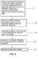
- the first general step, designated as block 21 is to form a multiple-level pattern of dielectric steps 4 on the surface of the conductive layer 3 of the carrier 1.
- the dielectric steps 4 are formed by embossing a polymer structure.
- the dielectric material is optically transparent and could be formed by alternative techniques, for example by micromoulding as taught in WO 96/35971.
- a trench 6 is formed in the dielectric structure 4. If necessary, the trench 6 is plasma-etched to remove polymer from the bottom of the trench 6. Metal, in this example nickel, is then electroplated into the trench 6 to form a busbar 8 ( Figure 1b) (block 22, Figure 8).
- the conductor 3 forms the cathode of an electrolytic cell with a nickel anode and standard nickel sulphamate-based electrolyte.
- Plating may be carried out with DC, with pulsed or biased AC current used to fill in the trenches 6 completely.
- Other known electro-deposition techniques may be employed. Suitable metals include nickel, copper and gold.
- the busbars 8 are linear structures which will run across the length or width of the display substrate to which they are transferred. They are typically about 100 ⁇ m apart and up to many metres in length. The busbars 8 are about 5 x 5 ⁇ m is cross-section and have a low resistance that in use will apply an applied voltage evenly across the device. The metal of the busbar 8 is opaque but it is small enough not to reduce the aperture too much.
- a transparent conductor 10 is deposited onto the dielectric structure 4 and busbars 8, as illustrated in Figure 1c.
- the conductor 10 may comprise indium oxide, tin oxide, indium tin oxide (ITO) or the like, but is preferably an organic conductor such as PEDOT:PSS (HC Starck Baytron P), which may be applied by a printing technique such as inkjet printing.
- PEDOT:PSS HC Starck Baytron P
- the transparent conductor is then selectively etched or bleached to provide transparent electrodes 10.
- Standard photolithographic techniques can be used to prevent the conductor contacting more than one busbar 8.
- PEDOT:PSS is selectively bleached by UV light to form the electrode structures.
- standard photoresists and etching or chemical deactivation may be employed.
- busbar 8 and electrode track 10 are shown.
- a plurality of similar dielectric structures, busbars and electrode structures will be formed, each electrode structure 10 typically comprising one of a series of parallel row or column electrodes.
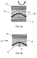
- the resulting structure is treated with a transparent transfer adhesive 14 and the final display substrate 12 is laminated and the adhesive 14 is cured ( Figure 2a) (block 24, Figure 8).
- the transfer adhesive 14 is a UV-curable material such as NOA81 (Norland Optical Products) but may be thermal- or moisture-cured.
- the display substrate 12 is preferably a plastics material, for example PEN (DuPont Teijin Teonex Q65), PES (Sumitomo Bakelite) or polyArylate (Ferrania SpA - Arylite), but could comprise glass, preferably a UV-translucent glass.
- the transfer carrier 1 is removed leaving the cell wall assembly 5.
- the adhesions in the assembly shown in Figure 2a are tuned such that when the transfer carrier 1 is peeled off, the adhesion breaks at the surface of the conducting carrier substrate 3.
- the whole of the rest of the structure remains adhered to the display substrate 12, as illustrated in the cell wall assembly 5 of Figure 2b. This surface is flat so that the resulting LC layer will be a constant thickness.
- the electrode structures 10, however, are embedded at different distances from the cell wall 12. The distances are set by the initial embossing of the dielectric structures 4 (now a dielectric covering layer for the electrode structures 10).
- one of the dielectric steps 4 is the full thickness of the busbar 8. It may be desirable to make the steps less than the full thickness of the busbar 8 to avoid increasing the switching threshold too much. The width of the step could be kept small to minimise the non-switching region.
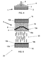
- the initial trench 6 may be made somewhat shallower and the metal may be overplated to form a busbar 8 that extends beyond the dielectric structures 4 as illustrated in Figure 4.
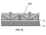
- the transfer carrier 1 of Figure 3a is similar to that of Figure 1a except that the embossing 4 includes additional raised lines or walls 101 (levees) which are significantly taller than the surrounding features and define the boundaries of the pixel or electrode line.
- the levees 101 are from 4 - 10 ⁇ m tall and 3 - 7 ⁇ m wide. Preferably they have a smooth surface to reduce the wetting of the subsequent coatings.
- the busbar 8 is formed in the trench 6 in a similar manner to that of Figure 1b.
- a liquid solvent-based transparent conductor 103 (eg a dispersion of PEDOT:PSS [HC Starck Baytron P]) is coated into the areas (channels or pixels) defined by the levees 101.
- the coating process may be any known deposition technique, preferably gravure or flexogravure coating, or inkjet deposition.
- the dispersion 103, in this example PEDOT:PSS dries and forms a substantially uniform layer 10 to form the transparent conductor.
- the surface properties of the embossing resin 4 are such that the film formation provides a uniform coating while preventing any coating over the levees 101.
- the layer 10 makes ohmic contact with the busbar 8.
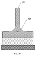
- the bottom corners of the levees 101 may include an internal radius 104 feature matched to minimise the meniscus effect forming an undesirable thicker conductive region closer to the levee.
- a display device with greyscale capability 22 comprises the cell wall assembly 5 of Figure 2b, including a first cell wall 12a and first electrode structures 10a, formed as previously described and in ohmic contact with the busbar 8.
- the device 22 in this example is a liquid crystal display device and has a layer of electro-optic material 20 which comprises a nematic LC.
- a first surface alignment 18a is provided on the innermost surface of the cell wall assembly 5.
- the surface alignment 18a in this example comprises a PABN surface textured with posts to provide bistable alignment to adjacent molecules of the nematic LC material 20.
- Other bistable alignments could be used, or conventional alignment materials such as rubbed polyimide if the display is monostable, for example a supertwist or HAN cell.
- a second cell wall 12b is of conventional construction, being formed from a flat glass or plastics material and having second electrode structures 10b formed thereon by a conventional etch technique using ITO.
- a second surface alignment 18b is provided on the second electrode structures 10b, in this example inducing homeotropic alignment in adjacent LC molecules.
- Means for distinguishing between different optical states are provided, in this example polarisers 16 which are adhered to the outer surfaces of the cell walls 12. It will be understood that surface alignments 18 could be transposed; ie the PABN surface alignment could be provided on the innermost surface of the second cell wall and the homeotropic surface alignment could be provided on the first cell wall assembly 5.
- the second cell wall 12b may be spaced apart from the first cell wall assembly 5 by conventional spacing means (not shown) for example microbeads or pieces of glass fibre or polymer fibre. Suitable spacing means are well known to those skilled in the art of LCD manufacture.
- both cell walls 12 are substantially planar and parallel to each other, and the layer of nematic LC material 20 is of substantially constant thickness.
- the shortest distance between the LC material 20 and one of the first electrode structures 10a varies within the area of the pixel illustrated in Figure 5. Above a maximum threshold voltage all of the visible pixel area is in an 'on' state. For a bistable display, when the voltage is reduced or removed the pixel remains in the ⁇ on' state. To switch the pixel to an ⁇ off' state, a suitable pulse is applied.
- the LCD of Figure 6 is similar to that of Figure 5 except that the second cell wall assembly 5b is constructed similarly to that of the first cell wall assembly 5a. Dielectric steps 4b separate the second electrode structures 10b from the LC 20.
- the second cell wall assembly 5b may be constructed by a similar transfer method to that used to make the first cell wall assembly 5a.
- the transparent adhesive 14b of the second cell wall assembly 5b may be formed of the same adhesive material as the transparent adhesive 14a of the first cell wall assembly.
- the shortest distance between the LC material 20 and one of the first electrode structures 10a varies within the area of the pixel, as does the shortest distance between the LC material 20 and one of the second electrode structures 4b.
- the cell may be symmetrical in a plane through the LC layer 20 parallel to the cell walls 12 and may be more easily constructed because the electrode variation may be shared between the two cell wall assemblies.
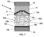
- FIG. 7 illustrates an alternative embodiment of a bistable LCD in which the polariser 16 on the upper cell wall 12a is provided on an inner surface, in this example between the first cell wall 12a and the adhesive 14, so that birefringence of the first cell wall 12a does not affect the display appearance.
- the switching voltage differs according to the shortest distance of the electrode structure 10a and the LC molecules 20.
- Each dielectric step 4 increases the switching threshold voltage.
- the electric field applied across the LC has to exceed a threshold.
- the applied voltage needed to switch the LC can be controlled by varying the thickness of the steps.
Landscapes
- Physics & Mathematics (AREA)
- Nonlinear Science (AREA)
- Mathematical Physics (AREA)
- Chemical & Material Sciences (AREA)
- Crystallography & Structural Chemistry (AREA)
- General Physics & Mathematics (AREA)
- Optics & Photonics (AREA)
- Spectroscopy & Molecular Physics (AREA)
- Liquid Crystal (AREA)
- Electrochromic Elements, Electrophoresis, Or Variable Reflection Or Absorption Elements (AREA)
- Devices For Indicating Variable Information By Combining Individual Elements (AREA)
- Gas-Filled Discharge Tubes (AREA)
Applications Claiming Priority (1)
| Application Number | Priority Date | Filing Date | Title |
|---|---|---|---|
| GB0423134A GB2419216A (en) | 2004-10-18 | 2004-10-18 | Display device with greyscale capability |
Publications (3)
| Publication Number | Publication Date |
|---|---|
| EP1674923A2 true EP1674923A2 (fr) | 2006-06-28 |
| EP1674923A3 EP1674923A3 (fr) | 2006-08-09 |
| EP1674923B1 EP1674923B1 (fr) | 2014-01-01 |
Family
ID=33462943
Family Applications (1)
| Application Number | Title | Priority Date | Filing Date |
|---|---|---|---|
| EP05104572.2A Expired - Lifetime EP1674923B1 (fr) | 2004-10-18 | 2005-05-27 | Dispositif d'affichage avec capabilité en niveaux de gris |
Country Status (4)
| Country | Link |
|---|---|
| US (1) | US8599326B2 (fr) |
| EP (1) | EP1674923B1 (fr) |
| JP (1) | JP4974505B2 (fr) |
| GB (1) | GB2419216A (fr) |
Cited By (2)
| Publication number | Priority date | Publication date | Assignee | Title |
|---|---|---|---|---|
| WO2007072355A3 (fr) * | 2005-12-20 | 2007-10-18 | Koninkl Philips Electronics Nv | Affichage électrophorétique à commutation dans le plan améliorée |
| WO2008014302A2 (fr) | 2006-07-28 | 2008-01-31 | Hewlett-Packard Development Company, L.P. | Couche à plusieurs niveaux |
Families Citing this family (9)
| Publication number | Priority date | Publication date | Assignee | Title |
|---|---|---|---|---|
| GB0523437D0 (en) * | 2005-11-17 | 2005-12-28 | Imp College Innovations Ltd | A method of patterning a thin film |
| US20080018576A1 (en) * | 2006-07-23 | 2008-01-24 | Peter James Fricke | Display element having groups of individually turned-on steps |
| US20080018673A1 (en) * | 2006-07-24 | 2008-01-24 | Peter James Fricke | Display element having substantially equally spaced human visual system (HVS) perceived lightness levels |
| US20080018577A1 (en) * | 2006-07-23 | 2008-01-24 | Peter James Fricke | Display element having individually turned-on steps |
| US7859498B2 (en) * | 2007-04-26 | 2010-12-28 | Hewlett-Packard Development Company, L.P. | Display device having multiplexing resistors within resin layer |
| US8130192B2 (en) * | 2007-06-15 | 2012-03-06 | Ricoh Co., Ltd. | Method for reducing image artifacts on electronic paper displays |
| EP2390403B1 (fr) * | 2010-05-28 | 2012-07-04 | Electrolux Home Products Corporation N.V. | Procédé d'assemblage de panneau d'un appareil, spécialement un appareil domestique |
| JP2012191156A (ja) * | 2011-02-25 | 2012-10-04 | Tokyo Electron Ltd | 配線の形成方法および形成装置 |
| CN107394062B (zh) * | 2017-07-20 | 2019-02-05 | 京东方科技集团股份有限公司 | 一种有机发光二极管显示面板及其制作方法、显示装置 |
Family Cites Families (30)
| Publication number | Priority date | Publication date | Assignee | Title |
|---|---|---|---|---|
| JPH079508B2 (ja) | 1985-01-18 | 1995-02-01 | キヤノン株式会社 | 液晶表示素子及びその駆動方法 |
| US4712877A (en) * | 1985-01-18 | 1987-12-15 | Canon Kabushiki Kaisha | Ferroelectric display panel of varying thickness and driving method therefor |
| JPH0799416B2 (ja) * | 1985-12-20 | 1995-10-25 | キヤノン株式会社 | 液晶装置 |
| JPH0723942B2 (ja) * | 1985-08-08 | 1995-03-15 | 株式会社半導体エネルギ−研究所 | 液晶装置 |
| JPS62262022A (ja) * | 1986-05-08 | 1987-11-14 | Matsushita Electric Ind Co Ltd | 電気光学効果を利用した装置 |
| US4763985A (en) | 1986-08-01 | 1988-08-16 | Minnesota Mining And Manufacturing Company | Retroreflective sheet with enhanced brightness |
| JPH0268520A (ja) * | 1988-09-02 | 1990-03-08 | Sharp Corp | 表示装置 |
| US5080467A (en) * | 1989-03-03 | 1992-01-14 | Greyhawk Systems, Inc | Biphenyl derivatives for photostabilization in pulsed optical darkening apparatus and method |
| DE3917472A1 (de) | 1989-05-30 | 1990-12-06 | Hoechst Ag | Ferroelektrisches fluessigkristalldisplay mit graustufen bzw. einer kontinuierlichen grauskala |
| JP2969839B2 (ja) | 1990-07-10 | 1999-11-02 | 株式会社デンソー | 液晶電気光学装置 |
| US5126865A (en) * | 1990-12-31 | 1992-06-30 | Honeywell Inc. | Liquid crystal display with sub-pixels |
| KR950004378B1 (ko) * | 1992-09-09 | 1995-04-28 | 주식회사금성사 | 위치감지액정표시소자및제조방법 |
| EP0588568B1 (fr) * | 1992-09-18 | 2002-12-18 | Hitachi, Ltd. | Dispositif d'affichage à cristal liquide |
| GB2293908A (en) | 1994-10-03 | 1996-04-10 | Sharp Kk | Liquid crystal display element |
| GB9615817D0 (en) * | 1996-07-26 | 1996-09-04 | Secr Defence | Liquid crystal device with greyscale |
| US6127199A (en) * | 1996-11-12 | 2000-10-03 | Seiko Epson Corporation | Manufacturing method of active matrix substrate, active matrix substrate and liquid crystal display device |
| JP3809733B2 (ja) | 1998-02-25 | 2006-08-16 | セイコーエプソン株式会社 | 薄膜トランジスタの剥離方法 |
| US6151153A (en) * | 1998-06-16 | 2000-11-21 | Photon Dynamics, Inc. | Modulator transfer process and assembly |
| US6503564B1 (en) * | 1999-02-26 | 2003-01-07 | 3M Innovative Properties Company | Method of coating microstructured substrates with polymeric layer(s), allowing preservation of surface feature profile |
| KR100312260B1 (ko) * | 1999-05-25 | 2001-11-03 | 구본준, 론 위라하디락사 | 액정표시장치 및 그 제조방법 |
| EP1067425B1 (fr) * | 1999-07-09 | 2008-12-17 | Hewlett-Packard Company, A Delaware Corporation | Dispositif d'affichage à cristaux liquide et son procédé de fabrication |
| EP1089113B1 (fr) * | 1999-09-28 | 2010-03-03 | Kyodo Printing Co., Ltd. | Elément de transfert et procédé d'utilisation |
| KR100641628B1 (ko) * | 2000-08-21 | 2006-11-02 | 엘지.필립스 엘시디 주식회사 | 블랙레진을 이용한 반사형 및 반투과형 액정표시장치 |
| JP4069620B2 (ja) | 2001-07-10 | 2008-04-02 | コニカミノルタホールディングス株式会社 | 熱現像写真感光材料及び画像形成方法 |
| US7317499B2 (en) * | 2002-08-22 | 2008-01-08 | Nitto Denko Corporation | Multilayer plate and display panel with anisotropic crystal film and conducting protective layer |
| US7271863B2 (en) * | 2002-10-16 | 2007-09-18 | Nitto Denko Corporation | Color liquid crystal display with internal rear polarizer |
| GB2394781B (en) * | 2002-10-31 | 2005-11-09 | Hewlett Packard Co | Bistable nematic liquid crystal display device |
| JP2005062724A (ja) * | 2003-08-20 | 2005-03-10 | Toshiba Matsushita Display Technology Co Ltd | 光学位相差板および液晶表示装置 |
| JP4007340B2 (ja) * | 2003-09-19 | 2007-11-14 | セイコーエプソン株式会社 | 電気光学装置、電子機器及び電気光学装置の製造方法 |
| US20060066803A1 (en) * | 2004-09-30 | 2006-03-30 | Aylward Peter T | Substrate free flexible liquid crystal displays |
-
2004
- 2004-10-18 GB GB0423134A patent/GB2419216A/en active Pending
-
2005
- 2005-05-27 EP EP05104572.2A patent/EP1674923B1/fr not_active Expired - Lifetime
- 2005-09-23 US US11/234,539 patent/US8599326B2/en not_active Expired - Fee Related
- 2005-10-17 JP JP2005301636A patent/JP4974505B2/ja not_active Expired - Fee Related
Cited By (4)
| Publication number | Priority date | Publication date | Assignee | Title |
|---|---|---|---|---|
| WO2007072355A3 (fr) * | 2005-12-20 | 2007-10-18 | Koninkl Philips Electronics Nv | Affichage électrophorétique à commutation dans le plan améliorée |
| WO2008014302A2 (fr) | 2006-07-28 | 2008-01-31 | Hewlett-Packard Development Company, L.P. | Couche à plusieurs niveaux |
| WO2008014302A3 (fr) * | 2006-07-28 | 2008-03-13 | Hewlett Packard Development Co | Couche à plusieurs niveaux |
| US9366895B2 (en) | 2006-07-28 | 2016-06-14 | Hewlett-Packard Development Company, L.P. | Liquid crystal display with polymer layer of varying thickness and method of producing such a layer |
Also Published As
| Publication number | Publication date |
|---|---|
| US8599326B2 (en) | 2013-12-03 |
| EP1674923A3 (fr) | 2006-08-09 |
| US20060082710A1 (en) | 2006-04-20 |
| EP1674923B1 (fr) | 2014-01-01 |
| GB2419216A (en) | 2006-04-19 |
| JP4974505B2 (ja) | 2012-07-11 |
| GB0423134D0 (en) | 2004-11-17 |
| JP2006119644A (ja) | 2006-05-11 |
Similar Documents
| Publication | Publication Date | Title |
|---|---|---|
| EP1674923B1 (fr) | Dispositif d'affichage avec capabilité en niveaux de gris | |
| EP1573389B1 (fr) | Panneaux arriere pour afficheurs electro-optiques | |
| US20120162745A1 (en) | Display | |
| EP0845696B1 (fr) | Elément d'affichage à cristaux liquides | |
| KR101386574B1 (ko) | 액정표시소자 | |
| KR20190060889A (ko) | 라미네이트된 전기-광학 디스플레이들 및 이를 제조하는 방법들 | |
| EP0385419A1 (fr) | Dispositif d'affichage à cristal liquide | |
| EP1728119B1 (fr) | Dispositif d'affichage couleur et son procede de production | |
| EP0772070A1 (fr) | Dispositif d'affichage à cristal liquide et son procédé de fabrication | |
| EP1728120B1 (fr) | Applications d' l ments de couleur et bus pour un substrat d'affichage | |
| EP1678551B1 (fr) | Ecrans electro-optiques | |
| KR101263659B1 (ko) | 전기영동 표시 장치 및 그 제조방법 | |
| CN100434993C (zh) | 将彩色元件和母线施加到显示基板的方法及其转移载体 | |
| JP3603656B2 (ja) | 表示用電極基板の製造方法 | |
| TWI915016B (zh) | 具有支撐結構的電泳式顯示器 | |
| JP2999367B2 (ja) | 表示装置およびその製造方法 | |
| JPH0922030A (ja) | 液晶表示装置 | |
| KR19980042840A (ko) | 액정 표시 소자 및 액정 표시 소자용 전극 기판의 제조 방법 | |
| KR20050060196A (ko) | 유연성을 갖는 표시 장치의 제조 방법 | |
| JPH04342207A (ja) | カラーフィルター及びその製造方法 | |
| KR19990011943A (ko) | 계조화 액정 표시 소자 | |
| JPH0862638A (ja) | 液晶表示装置の製造方法 | |
| WO2002067045A1 (fr) | Procede de modification de phase de cristaux liquides cholesteriques bistables | |
| JPH0854650A (ja) | 表示装置 | |
| KR20080103758A (ko) | 액정 표시 장치용 기판, 이를 포함하는 액정 표시 패널 및액정 표시 장치용 기판의 제조 방법 |
Legal Events
| Date | Code | Title | Description |
|---|---|---|---|
| PUAI | Public reference made under article 153(3) epc to a published international application that has entered the european phase |
Free format text: ORIGINAL CODE: 0009012 |
|
| AK | Designated contracting states |
Kind code of ref document: A2 Designated state(s): AT BE BG CH CY CZ DE DK EE ES FI FR GB GR HU IE IS IT LI LT LU MC NL PL PT RO SE SI SK TR |
|
| AX | Request for extension of the european patent |
Extension state: AL BA HR LV MK YU |
|
| PUAL | Search report despatched |
Free format text: ORIGINAL CODE: 0009013 |
|
| AK | Designated contracting states |
Kind code of ref document: A3 Designated state(s): AT BE BG CH CY CZ DE DK EE ES FI FR GB GR HU IE IS IT LI LT LU MC NL PL PT RO SE SI SK TR |
|
| AX | Request for extension of the european patent |
Extension state: AL BA HR LV MK YU |
|
| AKX | Designation fees paid | ||
| 17P | Request for examination filed |
Effective date: 20070216 |
|
| RBV | Designated contracting states (corrected) |
Designated state(s): DE FR GB |
|
| REG | Reference to a national code |
Ref country code: DE Ref legal event code: 8566 |
|
| 17Q | First examination report despatched |
Effective date: 20100120 |
|
| GRAP | Despatch of communication of intention to grant a patent |
Free format text: ORIGINAL CODE: EPIDOSNIGR1 |
|
| INTG | Intention to grant announced |
Effective date: 20130808 |
|
| GRAS | Grant fee paid |
Free format text: ORIGINAL CODE: EPIDOSNIGR3 |
|
| GRAA | (expected) grant |
Free format text: ORIGINAL CODE: 0009210 |
|
| AK | Designated contracting states |
Kind code of ref document: B1 Designated state(s): DE FR GB |
|
| REG | Reference to a national code |
Ref country code: GB Ref legal event code: FG4D |
|
| REG | Reference to a national code |
Ref country code: DE Ref legal event code: R096 Ref document number: 602005042330 Country of ref document: DE Effective date: 20140213 |
|
| REG | Reference to a national code |
Ref country code: DE Ref legal event code: R097 Ref document number: 602005042330 Country of ref document: DE |
|
| PLBE | No opposition filed within time limit |
Free format text: ORIGINAL CODE: 0009261 |
|
| STAA | Information on the status of an ep patent application or granted ep patent |
Free format text: STATUS: NO OPPOSITION FILED WITHIN TIME LIMIT |
|
| 26N | No opposition filed |
Effective date: 20141002 |
|
| REG | Reference to a national code |
Ref country code: DE Ref legal event code: R097 Ref document number: 602005042330 Country of ref document: DE Effective date: 20141002 |
|
| REG | Reference to a national code |
Ref country code: FR Ref legal event code: ST Effective date: 20150130 |
|
| PG25 | Lapsed in a contracting state [announced via postgrant information from national office to epo] |
Ref country code: FR Free format text: LAPSE BECAUSE OF NON-PAYMENT OF DUE FEES Effective date: 20140602 |
|
| PGFP | Annual fee paid to national office [announced via postgrant information from national office to epo] |
Ref country code: DE Payment date: 20150422 Year of fee payment: 11 Ref country code: GB Payment date: 20150424 Year of fee payment: 11 |
|
| REG | Reference to a national code |
Ref country code: DE Ref legal event code: R119 Ref document number: 602005042330 Country of ref document: DE |
|
| GBPC | Gb: european patent ceased through non-payment of renewal fee |
Effective date: 20160527 |
|
| PG25 | Lapsed in a contracting state [announced via postgrant information from national office to epo] |
Ref country code: DE Free format text: LAPSE BECAUSE OF NON-PAYMENT OF DUE FEES Effective date: 20161201 |
|
| PG25 | Lapsed in a contracting state [announced via postgrant information from national office to epo] |
Ref country code: GB Free format text: LAPSE BECAUSE OF NON-PAYMENT OF DUE FEES Effective date: 20160527 |