EP1677146A2 - Vorrichtung zur Herstellung einer Maske für die Plasmaätzung eines Halbleitersubstrats - Google Patents
Vorrichtung zur Herstellung einer Maske für die Plasmaätzung eines Halbleitersubstrats Download PDFInfo
- Publication number
- EP1677146A2 EP1677146A2 EP05112633A EP05112633A EP1677146A2 EP 1677146 A2 EP1677146 A2 EP 1677146A2 EP 05112633 A EP05112633 A EP 05112633A EP 05112633 A EP05112633 A EP 05112633A EP 1677146 A2 EP1677146 A2 EP 1677146A2
- Authority
- EP
- European Patent Office
- Prior art keywords
- screen
- substrate
- etched
- mask
- area
- Prior art date
- Legal status (The legal status is an assumption and is not a legal conclusion. Google has not performed a legal analysis and makes no representation as to the accuracy of the status listed.)
- Granted
Links
Images


Classifications
-
- G—PHYSICS
- G03—PHOTOGRAPHY; CINEMATOGRAPHY; ANALOGOUS TECHNIQUES USING WAVES OTHER THAN OPTICAL WAVES; ELECTROGRAPHY; HOLOGRAPHY
- G03F—PHOTOMECHANICAL PRODUCTION OF TEXTURED OR PATTERNED SURFACES, e.g. FOR PRINTING, FOR PROCESSING OF SEMICONDUCTOR DEVICES; MATERIALS THEREFOR; ORIGINALS THEREFOR; APPARATUS SPECIALLY ADAPTED THEREFOR
- G03F1/00—Originals for photomechanical production of textured or patterned surfaces, e.g., masks, photo-masks, reticles; Mask blanks or pellicles therefor; Containers specially adapted therefor; Preparation thereof
- G03F1/20—Masks or mask blanks for imaging by charged particle beam [CPB] radiation, e.g. by electron beam; Preparation thereof
Definitions
- the micromachining of the silicon substrates is currently carried out by plasma etching techniques, such as that described in document US Pat. No. 5,501,893.
- This technique consists in partially protecting the silicon substrate by an etching mask, and in submitting the substrate thus partially protected with an alternating succession of etching gas plasma etching steps and passivation plasma passivation steps.
- a pattern to be burned is transferred to the substrate from a transmission mask. The transfer is usually carried out by the photolithography technique of irradiating the substrate through the photon radiation transmission mask.
- the means for confining the ions comprises at least one screen made of conductive material disposed above the substrate and along the boundary separating the pattern area to be etched from the area not to be etched, said screen having the form of vertical plates arranged parallel to each side of the pattern area to be engraved quadrilateral.
- the substrate comprises a plurality of zones comprising patterns to be etched separated from each other by zones that must not be etched.
- a large number of patterns can be produced more quickly and cheaply.
- each area to be engraved is surrounded by its own screen.
- the screen is interrupted at the corners of the quadrilateral when the angle is distant from a piece of conductive material a distance less than or equal to the constant distance separating the screen of the boundary of the pattern area to be engraved to avoid edge effects.
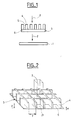
- the mask 3 is shown in perspective in FIG. 2. It comprises reliefs 4 with a depth p of 725 ⁇ m, for example.
- the small surface 5 carrying the pattern to be engraved is for example a square surface of 1.13 mm side.
- the surface 5 may further comprise holes of 120 nm in diameter, for example.
- the membrane 6 has a thickness e of 2 ⁇ m, for example.
- An electron beam 2 is sent on the mask 3. The beam 2 passes through the surface 5 to copy the pattern that it carries on the substrate.
- the device 30 for manufacturing plasma etching masks of a semiconductor substrate 31 according to the present invention is shown diagrammatically in FIG. 3.
- the masks once made are for example in the form of two rectangular zones 31a and 31b. b of etched patterns in the substrate 31, surrounded by a zone 31 c which has not been etched.
- the zones 31a and 31b have, for example, a length of 132.57mm and a width of 54.43mm, and carry a pattern in a network.
Landscapes
- Physics & Mathematics (AREA)
- General Physics & Mathematics (AREA)
- Electron Beam Exposure (AREA)
- Drying Of Semiconductors (AREA)
- Preparing Plates And Mask In Photomechanical Process (AREA)
Applications Claiming Priority (1)
| Application Number | Priority Date | Filing Date | Title |
|---|---|---|---|
| FR0550002A FR2880469B1 (fr) | 2005-01-03 | 2005-01-03 | Dispositif de fabrication d'un masque par gravure par plasma d'un substrat semiconducteur |
Publications (3)
| Publication Number | Publication Date |
|---|---|
| EP1677146A2 true EP1677146A2 (de) | 2006-07-05 |
| EP1677146A3 EP1677146A3 (de) | 2007-03-28 |
| EP1677146B1 EP1677146B1 (de) | 2012-09-19 |
Family
ID=34953717
Family Applications (1)
| Application Number | Title | Priority Date | Filing Date |
|---|---|---|---|
| EP05112633A Expired - Lifetime EP1677146B1 (de) | 2005-01-03 | 2005-12-21 | Vorrichtung zur Herstellung einer Maske für die Plasmaätzung eines Halbleitersubstrats |
Country Status (5)
| Country | Link |
|---|---|
| US (1) | US7938907B2 (de) |
| EP (1) | EP1677146B1 (de) |
| JP (1) | JP5075337B2 (de) |
| CN (1) | CN100382250C (de) |
| FR (1) | FR2880469B1 (de) |
Families Citing this family (1)
| Publication number | Priority date | Publication date | Assignee | Title |
|---|---|---|---|---|
| KR101084268B1 (ko) * | 2009-09-25 | 2011-11-16 | 삼성모바일디스플레이주식회사 | 기판 센터링 장치 및 이를 구비한 유기물 증착 시스템 |
Citations (2)
| Publication number | Priority date | Publication date | Assignee | Title |
|---|---|---|---|---|
| US5501893A (en) | 1992-12-05 | 1996-03-26 | Robert Bosch Gmbh | Method of anisotropically etching silicon |
| US6352802B1 (en) | 1999-05-28 | 2002-03-05 | Nec Corporation | Mask for electron beam exposure and method of manufacturing semiconductor device using the same |
Family Cites Families (12)
| Publication number | Priority date | Publication date | Assignee | Title |
|---|---|---|---|---|
| US3887421A (en) * | 1973-01-22 | 1975-06-03 | Gen Motors Corp | Method of masking semiconductor wafers using a self-aligning mask |
| JPS63151948A (ja) * | 1986-12-15 | 1988-06-24 | Nec Corp | 露光用マスク |
| US5891348A (en) * | 1996-01-26 | 1999-04-06 | Applied Materials, Inc. | Process gas focusing apparatus and method |
| JPH09246251A (ja) * | 1996-03-01 | 1997-09-19 | Sony Corp | 半導体製造装置及び半導体製造方法 |
| JPH1174252A (ja) * | 1997-08-28 | 1999-03-16 | Sony Corp | 半導体装置および製造方法 |
| US6383938B2 (en) * | 1999-04-21 | 2002-05-07 | Alcatel | Method of anisotropic etching of substrates |
| JP2001007013A (ja) * | 1999-06-24 | 2001-01-12 | Nikon Corp | 転写マスクブランクス及びその製造方法 |
| JP2002299226A (ja) * | 2001-04-03 | 2002-10-11 | Nikon Corp | 電子線露光用ステンシルマスク及びその作製方法 |
| JP2002329711A (ja) * | 2001-05-01 | 2002-11-15 | Matsushita Electric Ind Co Ltd | 平行平板型電極プラズマ処理装置 |
| FR2834382B1 (fr) * | 2002-01-03 | 2005-03-18 | Cit Alcatel | Procede et dispositif de gravure anisotrope du silicium a haut facteur d'aspect |
| JP2003273002A (ja) * | 2002-03-14 | 2003-09-26 | Sony Corp | マスクの製造方法 |
| US6960263B2 (en) * | 2002-04-25 | 2005-11-01 | Applied Materials, Inc. | Shadow frame with cross beam for semiconductor equipment |
-
2005
- 2005-01-03 FR FR0550002A patent/FR2880469B1/fr not_active Expired - Fee Related
- 2005-12-21 EP EP05112633A patent/EP1677146B1/de not_active Expired - Lifetime
- 2005-12-26 JP JP2005371907A patent/JP5075337B2/ja not_active Expired - Fee Related
- 2005-12-29 US US11/319,630 patent/US7938907B2/en active Active
-
2006
- 2006-01-04 CN CNB2006100003062A patent/CN100382250C/zh not_active Expired - Lifetime
Patent Citations (2)
| Publication number | Priority date | Publication date | Assignee | Title |
|---|---|---|---|---|
| US5501893A (en) | 1992-12-05 | 1996-03-26 | Robert Bosch Gmbh | Method of anisotropically etching silicon |
| US6352802B1 (en) | 1999-05-28 | 2002-03-05 | Nec Corporation | Mask for electron beam exposure and method of manufacturing semiconductor device using the same |
Also Published As
| Publication number | Publication date |
|---|---|
| US20060148274A1 (en) | 2006-07-06 |
| FR2880469A1 (fr) | 2006-07-07 |
| CN1801462A (zh) | 2006-07-12 |
| JP5075337B2 (ja) | 2012-11-21 |
| CN100382250C (zh) | 2008-04-16 |
| EP1677146B1 (de) | 2012-09-19 |
| EP1677146A3 (de) | 2007-03-28 |
| FR2880469B1 (fr) | 2007-04-27 |
| JP2006191043A (ja) | 2006-07-20 |
| US7938907B2 (en) | 2011-05-10 |
Similar Documents
| Publication | Publication Date | Title |
|---|---|---|
| EP2434533B1 (de) | Molekulare verbindung mit reduzierten overlay fehlausrichtung | |
| US10599052B2 (en) | Vacuum system, in particular EUV lithography system, and optical element | |
| EP3508916B1 (de) | Herstellungsmethode einer mehrstufigen mikroform für die galvanoformung | |
| EP3728109B1 (de) | Verfahren zur herstellung von halbleiterbauelementen und vereinzelungslinien | |
| US20180207725A1 (en) | System and method for fabricating 3d metal structure | |
| Vila-Comamala et al. | Dense high aspect ratio hydrogen silsesquioxane nanostructures by 100 keV electron beam lithography | |
| FR2972848A1 (fr) | Appareil et procédé de collage par adhésion moléculaire avec minimisation de déformations locales | |
| EP1677146B1 (de) | Vorrichtung zur Herstellung einer Maske für die Plasmaätzung eines Halbleitersubstrats | |
| EP2040875B1 (de) | Verfahren und vorrichtung zur bearbeitung eines ziels mit femtosekunden-laserstrahl | |
| EP2883110B1 (de) | Substrat für hochauflösende elektronische lithografie und entsprechendes lithografieverfahren | |
| EP1461142B1 (de) | Verfahren zum herstellen einer folie mit durchgängigen poren und deren anwendung zur herstellung von mikron-und submikronfiltern | |
| FR2893018A1 (fr) | Procede de formation de supports presentant des motifs, tels que des masques de lithographie. | |
| EP4205177B1 (de) | Verfahren zur herstellung einer optoelektronischen vorrichtung | |
| US20240313172A1 (en) | Production method and optoelectronic semiconductor chip | |
| EP3252830A1 (de) | Verfahren zur herstellung von mustern unter verwendung von ionenimplantationen | |
| EP2219203B1 (de) | Verfahren zur Korrektur von Astigmatismus bei Bildgebungsverfahren durch Spektromikroskopie mit Elektronenemission | |
| EP3655821B1 (de) | Interferenzlithographie -verfahren und -system | |
| FR3073081B1 (fr) | Substrat semi-conducteur protege pour son transport et sa manipulation | |
| EP1803031B1 (de) | Reflektierende lithographiemaske und verfahren zu deren herstellung | |
| WO2017009564A1 (fr) | Pochoir et procédé de fabrication du pochoir | |
| TWI859680B (zh) | 晶圓表面處理方法 | |
| FR3091006A1 (fr) | Procede de remplissage selectif, par un liquide de remplissage, d’un groupe de cavites parmi une pluralite de cavites | |
| WO2023151852A1 (fr) | Procede de transfert d'une couche mince sur un substrat support | |
| WO2025132172A1 (fr) | Système à dispositifs optoélectroniques et procédé adapté de fabrication | |
| WO2001053891A1 (fr) | Procede de lithographie ionique, revetement a fort contraste, equipement et reticule de mise en oeuvre |
Legal Events
| Date | Code | Title | Description |
|---|---|---|---|
| PUAI | Public reference made under article 153(3) epc to a published international application that has entered the european phase |
Free format text: ORIGINAL CODE: 0009012 |
|
| AK | Designated contracting states |
Kind code of ref document: A2 Designated state(s): AT BE BG CH CY CZ DE DK EE ES FI FR GB GR HU IE IS IT LI LT LU LV MC NL PL PT RO SE SI SK TR |
|
| AX | Request for extension of the european patent |
Extension state: AL BA HR MK YU |
|
| PUAL | Search report despatched |
Free format text: ORIGINAL CODE: 0009013 |
|
| AK | Designated contracting states |
Kind code of ref document: A3 Designated state(s): AT BE BG CH CY CZ DE DK EE ES FI FR GB GR HU IE IS IT LI LT LU LV MC NL PL PT RO SE SI SK TR |
|
| AX | Request for extension of the european patent |
Extension state: AL BA HR MK YU |
|
| RIC1 | Information provided on ipc code assigned before grant |
Ipc: H01J 37/32 20060101AFI20070221BHEP Ipc: G03F 1/14 20060101ALI20070221BHEP |
|
| RAP1 | Party data changed (applicant data changed or rights of an application transferred) |
Owner name: ALCATEL LUCENT |
|
| 17P | Request for examination filed |
Effective date: 20070928 |
|
| AKX | Designation fees paid |
Designated state(s): AT BE BG CH CY CZ DE DK EE ES FI FR GB GR HU IE IS IT LI LT LU LV MC NL PL PT RO SE SI SK TR |
|
| REG | Reference to a national code |
Ref country code: DE Ref legal event code: R079 Ref document number: 602005036171 Country of ref document: DE Free format text: PREVIOUS MAIN CLASS: G03F0001140000 Ipc: G03F0001200000 |
|
| RAP1 | Party data changed (applicant data changed or rights of an application transferred) |
Owner name: ALCATEL LUCENT |
|
| RIC1 | Information provided on ipc code assigned before grant |
Ipc: H01J 37/32 20060101ALI20120221BHEP Ipc: G03F 1/20 20120101AFI20120221BHEP |
|
| GRAP | Despatch of communication of intention to grant a patent |
Free format text: ORIGINAL CODE: EPIDOSNIGR1 |
|
| GRAS | Grant fee paid |
Free format text: ORIGINAL CODE: EPIDOSNIGR3 |
|
| GRAA | (expected) grant |
Free format text: ORIGINAL CODE: 0009210 |
|
| AK | Designated contracting states |
Kind code of ref document: B1 Designated state(s): AT BE BG CH CY CZ DE DK EE ES FI FR GB GR HU IE IS IT LI LT LU LV MC NL PL PT RO SE SI SK TR |
|
| REG | Reference to a national code |
Ref country code: GB Ref legal event code: FG4D Free format text: NOT ENGLISH Ref country code: DE Ref legal event code: R081 Ref document number: 602005036171 Country of ref document: DE Owner name: WSOU INVESTMENTS, LLC, LOS ANGELES, US Free format text: FORMER OWNER: ALCATEL, PARIS, FR |
|
| REG | Reference to a national code |
Ref country code: CH Ref legal event code: EP |
|
| REG | Reference to a national code |
Ref country code: IE Ref legal event code: FG4D Free format text: LANGUAGE OF EP DOCUMENT: FRENCH |
|
| REG | Reference to a national code |
Ref country code: AT Ref legal event code: REF Ref document number: 576299 Country of ref document: AT Kind code of ref document: T Effective date: 20121015 |
|
| REG | Reference to a national code |
Ref country code: DE Ref legal event code: R096 Ref document number: 602005036171 Country of ref document: DE Effective date: 20121115 |
|
| PG25 | Lapsed in a contracting state [announced via postgrant information from national office to epo] |
Ref country code: LT Free format text: LAPSE BECAUSE OF FAILURE TO SUBMIT A TRANSLATION OF THE DESCRIPTION OR TO PAY THE FEE WITHIN THE PRESCRIBED TIME-LIMIT Effective date: 20120919 Ref country code: CY Free format text: LAPSE BECAUSE OF FAILURE TO SUBMIT A TRANSLATION OF THE DESCRIPTION OR TO PAY THE FEE WITHIN THE PRESCRIBED TIME-LIMIT Effective date: 20120919 Ref country code: FI Free format text: LAPSE BECAUSE OF FAILURE TO SUBMIT A TRANSLATION OF THE DESCRIPTION OR TO PAY THE FEE WITHIN THE PRESCRIBED TIME-LIMIT Effective date: 20120919 |
|
| REG | Reference to a national code |
Ref country code: NL Ref legal event code: VDEP Effective date: 20120919 |
|
| REG | Reference to a national code |
Ref country code: AT Ref legal event code: MK05 Ref document number: 576299 Country of ref document: AT Kind code of ref document: T Effective date: 20120919 |
|
| REG | Reference to a national code |
Ref country code: LT Ref legal event code: MG4D Effective date: 20120919 |
|
| PG25 | Lapsed in a contracting state [announced via postgrant information from national office to epo] |
Ref country code: GR Free format text: LAPSE BECAUSE OF FAILURE TO SUBMIT A TRANSLATION OF THE DESCRIPTION OR TO PAY THE FEE WITHIN THE PRESCRIBED TIME-LIMIT Effective date: 20121220 Ref country code: LV Free format text: LAPSE BECAUSE OF FAILURE TO SUBMIT A TRANSLATION OF THE DESCRIPTION OR TO PAY THE FEE WITHIN THE PRESCRIBED TIME-LIMIT Effective date: 20120919 Ref country code: SI Free format text: LAPSE BECAUSE OF FAILURE TO SUBMIT A TRANSLATION OF THE DESCRIPTION OR TO PAY THE FEE WITHIN THE PRESCRIBED TIME-LIMIT Effective date: 20120919 Ref country code: SE Free format text: LAPSE BECAUSE OF FAILURE TO SUBMIT A TRANSLATION OF THE DESCRIPTION OR TO PAY THE FEE WITHIN THE PRESCRIBED TIME-LIMIT Effective date: 20120919 |
|
| PG25 | Lapsed in a contracting state [announced via postgrant information from national office to epo] |
Ref country code: EE Free format text: LAPSE BECAUSE OF FAILURE TO SUBMIT A TRANSLATION OF THE DESCRIPTION OR TO PAY THE FEE WITHIN THE PRESCRIBED TIME-LIMIT Effective date: 20120919 Ref country code: ES Free format text: LAPSE BECAUSE OF FAILURE TO SUBMIT A TRANSLATION OF THE DESCRIPTION OR TO PAY THE FEE WITHIN THE PRESCRIBED TIME-LIMIT Effective date: 20121230 Ref country code: NL Free format text: LAPSE BECAUSE OF FAILURE TO SUBMIT A TRANSLATION OF THE DESCRIPTION OR TO PAY THE FEE WITHIN THE PRESCRIBED TIME-LIMIT Effective date: 20120919 Ref country code: CZ Free format text: LAPSE BECAUSE OF FAILURE TO SUBMIT A TRANSLATION OF THE DESCRIPTION OR TO PAY THE FEE WITHIN THE PRESCRIBED TIME-LIMIT Effective date: 20120919 Ref country code: RO Free format text: LAPSE BECAUSE OF FAILURE TO SUBMIT A TRANSLATION OF THE DESCRIPTION OR TO PAY THE FEE WITHIN THE PRESCRIBED TIME-LIMIT Effective date: 20120919 Ref country code: IS Free format text: LAPSE BECAUSE OF FAILURE TO SUBMIT A TRANSLATION OF THE DESCRIPTION OR TO PAY THE FEE WITHIN THE PRESCRIBED TIME-LIMIT Effective date: 20130119 |
|
| PG25 | Lapsed in a contracting state [announced via postgrant information from national office to epo] |
Ref country code: PT Free format text: LAPSE BECAUSE OF FAILURE TO SUBMIT A TRANSLATION OF THE DESCRIPTION OR TO PAY THE FEE WITHIN THE PRESCRIBED TIME-LIMIT Effective date: 20130121 Ref country code: PL Free format text: LAPSE BECAUSE OF FAILURE TO SUBMIT A TRANSLATION OF THE DESCRIPTION OR TO PAY THE FEE WITHIN THE PRESCRIBED TIME-LIMIT Effective date: 20120919 Ref country code: SK Free format text: LAPSE BECAUSE OF FAILURE TO SUBMIT A TRANSLATION OF THE DESCRIPTION OR TO PAY THE FEE WITHIN THE PRESCRIBED TIME-LIMIT Effective date: 20120919 |
|
| PG25 | Lapsed in a contracting state [announced via postgrant information from national office to epo] |
Ref country code: AT Free format text: LAPSE BECAUSE OF FAILURE TO SUBMIT A TRANSLATION OF THE DESCRIPTION OR TO PAY THE FEE WITHIN THE PRESCRIBED TIME-LIMIT Effective date: 20120919 |
|
| BERE | Be: lapsed |
Owner name: ALCATEL LUCENT Effective date: 20121231 |
|
| PLBE | No opposition filed within time limit |
Free format text: ORIGINAL CODE: 0009261 |
|
| STAA | Information on the status of an ep patent application or granted ep patent |
Free format text: STATUS: NO OPPOSITION FILED WITHIN TIME LIMIT |
|
| PG25 | Lapsed in a contracting state [announced via postgrant information from national office to epo] |
Ref country code: DK Free format text: LAPSE BECAUSE OF FAILURE TO SUBMIT A TRANSLATION OF THE DESCRIPTION OR TO PAY THE FEE WITHIN THE PRESCRIBED TIME-LIMIT Effective date: 20120919 Ref country code: MC Free format text: LAPSE BECAUSE OF NON-PAYMENT OF DUE FEES Effective date: 20121231 Ref country code: BG Free format text: LAPSE BECAUSE OF FAILURE TO SUBMIT A TRANSLATION OF THE DESCRIPTION OR TO PAY THE FEE WITHIN THE PRESCRIBED TIME-LIMIT Effective date: 20121219 |
|
| REG | Reference to a national code |
Ref country code: CH Ref legal event code: PL |
|
| 26N | No opposition filed |
Effective date: 20130620 |
|
| PG25 | Lapsed in a contracting state [announced via postgrant information from national office to epo] |
Ref country code: IT Free format text: LAPSE BECAUSE OF FAILURE TO SUBMIT A TRANSLATION OF THE DESCRIPTION OR TO PAY THE FEE WITHIN THE PRESCRIBED TIME-LIMIT Effective date: 20120919 |
|
| REG | Reference to a national code |
Ref country code: IE Ref legal event code: MM4A |
|
| PG25 | Lapsed in a contracting state [announced via postgrant information from national office to epo] |
Ref country code: BE Free format text: LAPSE BECAUSE OF NON-PAYMENT OF DUE FEES Effective date: 20121231 |
|
| REG | Reference to a national code |
Ref country code: DE Ref legal event code: R097 Ref document number: 602005036171 Country of ref document: DE Effective date: 20130620 |
|
| PG25 | Lapsed in a contracting state [announced via postgrant information from national office to epo] |
Ref country code: CH Free format text: LAPSE BECAUSE OF NON-PAYMENT OF DUE FEES Effective date: 20121231 Ref country code: IE Free format text: LAPSE BECAUSE OF NON-PAYMENT OF DUE FEES Effective date: 20121221 Ref country code: LI Free format text: LAPSE BECAUSE OF NON-PAYMENT OF DUE FEES Effective date: 20121231 |
|
| REG | Reference to a national code |
Ref country code: FR Ref legal event code: GC Effective date: 20131018 |
|
| PG25 | Lapsed in a contracting state [announced via postgrant information from national office to epo] |
Ref country code: TR Free format text: LAPSE BECAUSE OF FAILURE TO SUBMIT A TRANSLATION OF THE DESCRIPTION OR TO PAY THE FEE WITHIN THE PRESCRIBED TIME-LIMIT Effective date: 20120919 |
|
| PG25 | Lapsed in a contracting state [announced via postgrant information from national office to epo] |
Ref country code: LU Free format text: LAPSE BECAUSE OF NON-PAYMENT OF DUE FEES Effective date: 20121221 |
|
| PG25 | Lapsed in a contracting state [announced via postgrant information from national office to epo] |
Ref country code: HU Free format text: LAPSE BECAUSE OF FAILURE TO SUBMIT A TRANSLATION OF THE DESCRIPTION OR TO PAY THE FEE WITHIN THE PRESCRIBED TIME-LIMIT Effective date: 20051221 |
|
| REG | Reference to a national code |
Ref country code: FR Ref legal event code: RG Effective date: 20141016 |
|
| REG | Reference to a national code |
Ref country code: FR Ref legal event code: PLFP Year of fee payment: 11 |
|
| REG | Reference to a national code |
Ref country code: FR Ref legal event code: PLFP Year of fee payment: 12 |
|
| REG | Reference to a national code |
Ref country code: FR Ref legal event code: PLFP Year of fee payment: 13 |
|
| REG | Reference to a national code |
Ref country code: DE Ref legal event code: R082 Ref document number: 602005036171 Country of ref document: DE Representative=s name: METACOM LEGAL RECHTSANWAELTE, DE Ref country code: DE Ref legal event code: R082 Ref document number: 602005036171 Country of ref document: DE Representative=s name: METACOM LEGAL, DE Ref country code: DE Ref legal event code: R081 Ref document number: 602005036171 Country of ref document: DE Owner name: WSOU INVESTMENTS, LLC, LOS ANGELES, US Free format text: FORMER OWNER: ALCATEL LUCENT, PARIS, FR Ref country code: DE Ref legal event code: R082 Ref document number: 602005036171 Country of ref document: DE Representative=s name: BARKHOFF REIMANN VOSSIUS, DE |
|
| REG | Reference to a national code |
Ref country code: GB Ref legal event code: 732E Free format text: REGISTERED BETWEEN 20200924 AND 20200930 |
|
| REG | Reference to a national code |
Ref country code: DE Ref legal event code: R082 Ref document number: 602005036171 Country of ref document: DE Representative=s name: METACOM LEGAL RECHTSANWAELTE, DE Ref country code: DE Ref legal event code: R082 Ref document number: 602005036171 Country of ref document: DE Representative=s name: METACOM LEGAL, DE Ref country code: DE Ref legal event code: R082 Ref document number: 602005036171 Country of ref document: DE Representative=s name: METACOM LEGAL NAGEL MARKOWSKY VOSSIUS RECHTSAN, DE |
|
| P01 | Opt-out of the competence of the unified patent court (upc) registered |
Effective date: 20230606 |
|
| PGFP | Annual fee paid to national office [announced via postgrant information from national office to epo] |
Ref country code: DE Payment date: 20250529 Year of fee payment: 20 |
|
| PGFP | Annual fee paid to national office [announced via postgrant information from national office to epo] |
Ref country code: GB Payment date: 20250527 Year of fee payment: 20 |
|
| PGFP | Annual fee paid to national office [announced via postgrant information from national office to epo] |
Ref country code: FR Payment date: 20250526 Year of fee payment: 20 |
|
| REG | Reference to a national code |
Ref country code: DE Ref legal event code: R071 Ref document number: 602005036171 Country of ref document: DE |
|
| REG | Reference to a national code |
Ref country code: GB Ref legal event code: PE20 Expiry date: 20251220 |