EP3655821B1 - Interferenzlithographie -verfahren und -system - Google Patents
Interferenzlithographie -verfahren und -system Download PDFInfo
- Publication number
- EP3655821B1 EP3655821B1 EP18737918.5A EP18737918A EP3655821B1 EP 3655821 B1 EP3655821 B1 EP 3655821B1 EP 18737918 A EP18737918 A EP 18737918A EP 3655821 B1 EP3655821 B1 EP 3655821B1
- Authority
- EP
- European Patent Office
- Prior art keywords
- beams
- prism
- substrate
- interference
- resin
- Prior art date
- Legal status (The legal status is an assumption and is not a legal conclusion. Google has not performed a legal analysis and makes no representation as to the accuracy of the status listed.)
- Active
Links
Images


Classifications
-
- G—PHYSICS
- G03—PHOTOGRAPHY; CINEMATOGRAPHY; ANALOGOUS TECHNIQUES USING WAVES OTHER THAN OPTICAL WAVES; ELECTROGRAPHY; HOLOGRAPHY
- G03F—PHOTOMECHANICAL PRODUCTION OF TEXTURED OR PATTERNED SURFACES, e.g. FOR PRINTING, FOR PROCESSING OF SEMICONDUCTOR DEVICES; MATERIALS THEREFOR; ORIGINALS THEREFOR; APPARATUS SPECIALLY ADAPTED THEREFOR
- G03F7/00—Photomechanical, e.g. photolithographic, production of textured or patterned surfaces, e.g. printing surfaces; Materials therefor, e.g. comprising photoresists; Apparatus specially adapted therefor
- G03F7/70—Microphotolithographic exposure; Apparatus therefor
- G03F7/70408—Interferometric lithography; Holographic lithography; Self-imaging lithography, e.g. utilizing the Talbot effect
-
- G—PHYSICS
- G03—PHOTOGRAPHY; CINEMATOGRAPHY; ANALOGOUS TECHNIQUES USING WAVES OTHER THAN OPTICAL WAVES; ELECTROGRAPHY; HOLOGRAPHY
- G03F—PHOTOMECHANICAL PRODUCTION OF TEXTURED OR PATTERNED SURFACES, e.g. FOR PRINTING, FOR PROCESSING OF SEMICONDUCTOR DEVICES; MATERIALS THEREFOR; ORIGINALS THEREFOR; APPARATUS SPECIALLY ADAPTED THEREFOR
- G03F7/00—Photomechanical, e.g. photolithographic, production of textured or patterned surfaces, e.g. printing surfaces; Materials therefor, e.g. comprising photoresists; Apparatus specially adapted therefor
- G03F7/70—Microphotolithographic exposure; Apparatus therefor
- G03F7/70425—Imaging strategies, e.g. for increasing throughput or resolution, printing product fields larger than the image field or compensating lithography- or non-lithography errors, e.g. proximity correction, mix-and-match, stitching or double patterning
- G03F7/70466—Multiple exposures, e.g. combination of fine and coarse exposures, double patterning or multiple exposures for printing a single feature
-
- G—PHYSICS
- G03—PHOTOGRAPHY; CINEMATOGRAPHY; ANALOGOUS TECHNIQUES USING WAVES OTHER THAN OPTICAL WAVES; ELECTROGRAPHY; HOLOGRAPHY
- G03F—PHOTOMECHANICAL PRODUCTION OF TEXTURED OR PATTERNED SURFACES, e.g. FOR PRINTING, FOR PROCESSING OF SEMICONDUCTOR DEVICES; MATERIALS THEREFOR; ORIGINALS THEREFOR; APPARATUS SPECIALLY ADAPTED THEREFOR
- G03F9/00—Registration or positioning of originals, masks, frames, photographic sheets or textured or patterned surfaces, e.g. automatically
- G03F9/70—Registration or positioning of originals, masks, frames, photographic sheets or textured or patterned surfaces, e.g. automatically for microlithography
- G03F9/7092—Signal processing
Definitions
- the invention generally relates to the field of the structuring of substrates by interference lithography, also known as holographic lithography. More particularly, the invention relates to the use of interference lithography for the manufacture of metallic meso- or nanostructures on substrates, in particular with a view to producing sensors for plasmonics.
- the field of plasmonics is based on the interaction between a light beam and the free electron material electrons (metal or heavily doped semiconductor), often in the form of nanoparticles, nanostructures or nanostructured surfaces. These metal structures are mainly used in the field of sensors and detection of pollutants but also sensors of biological markers of pathologies (proteins, etc.).
- SERS technique for Surface Enhanced Raman Spectroscopy, which detects molecules present in a solution that are deposited on a surface by enhancing their Raman response or even the SEIRA for Surface Enhanced InfraRed Absorption.
- Optical lithography This technique typically employed in microelectronics consists in illuminating a photosensitive resin with a monochromatic optical source through a mask which has the shape of the desired structures / particles (positive resin), or a complementary shape (negative resin). It is limited in resolution both by the properties of the resin, and by the wavelength of the beam used.
- the wavelengths used today are in the deep UV (190 nm) or EUV (12 nm) would be compatible with the typical dimensions of plasmonic structures (50 nm), however the cost of instruments and methods is prohibitive. for the production of large disposable nanostructured surfaces (or consumables) for plasmonic sensors and of course requires the manufacture of specific masks.
- Lithography by nanospheres This process was the first used to produce shape-controlled plasmon structures. It consists of self-organizing nano-spheres on the sample, followed by evaporation of the desired metal and removal of the nano-spheres. Metal nanoparticles are obtained in the interstices of the network of nanospheres and consequently the shapes of structures obtained are typically limited to triangles. This technique is simple, compatible on a large scale but limited by the absence of order at large distances on micron scales (typically 10 to 20 times the size of the beads).
- Interferential lithography consists in creating an interference pattern on the surface of a photosensitive material. This technique is compatible with a large surface to be structured and allows the production of patterns of various shapes and geometry. This technique is limited to producing a periodic or quasi-periodic structure with a minimum spacing equal to half the wavelength of the laser. Size on the other hand, structures are not limited and can be adjusted depending on the dose and the properties of the resin. However, it is possible to reduce the spacing of the structures by working in immersion, ie by changing the refractive index of the medium. It should also be noted that interference lithography by the use of interference figures potentially makes it possible to obtain the most regular structures achievable over large surfaces. The main limitation comes from the quality of the extended laser beams.
- 'Three beam interference lithography upgrading a Lloyd's interferometer for single-exposure hexagonal patterning', OPTICS LETTERS, OPTICAL SOCIETY OF AMERICA, vol.34, no.12, 2009-06-15, pages 1783-1785 ; and Ngoc D lai et Al.: 'Fabrication of two- and three-dimensional quasi-periodic structures with 12-fold symmetry by interference technique', Optics express, 2006-10-30, pages 10746-1953 .
- the interference lithography technique is above all a masking technique and must be combined with transfer techniques such as etching or the lift-off process, as for the two previous techniques.
- the FR 2 964 469 describes the production of particularly interesting patterns with limited symmetry.
- a sensor comprising a substrate having a face comprising nanoparticles having the shape of a star with three branches. These stars are made of a metallic and / or semiconductor material and have dimensions of the order of a nanometer to a few tens of micrometers.
- This star structure proposed in the FR 2 964 469 is very advantageous, because it has been observed that the intensity of the plasmon resonance for a particle having the shape of a star with three branches, varies very weakly whatever the angle of polarization. This weak variation in intensity induces a sufficient and interesting independence of all the properties of the particle with respect to polarization.
- several advantages are linked to the use of particles having an order of symmetry greater than or equal to three: firstly, a large variety of shapes meet this definition; hence very great flexibility both in the architecture and in the geometry of the particles used. This makes it possible to obtain field enhancement factors much higher than those obtained with cylindrical or spherical particles, the radius of curvature of which is too large to allow effective enhancement.
- FR 2 964 469 The manufacturing method described in FR 2 964 469 is electronic lithography. As discussed above, this technique allows precise control of the geometry of structures and good reproducibility. Electronic lithography, or focused ion lithography, has therefore been widely used for the production of nano-hole arrays. But electron lithography and focused ion lithography are unsuitable due to their slowness for structuring large surfaces in the context of mass production.
- the present invention relates to a method of manufacturing structures with limited symmetry by interference lithography comprising a step of exposure by interference lithography of a photosensitive material placed on a substrate.
- the exposure step comprises at least three successive interference exposures carried out with three coplanar light beams, emitted by an optical system so as to interfere together on the same part of the photosensitive material, called the exposure surface.
- a relative rotation is carried out between the optical system and the substrate between the first and the second interference exposure, then between the second and the third interference exposure.
- One merit of the present inventors is to have developed, in a surprising and unpredictable manner, an exposure step by interference lithography making it possible to produce complex geometric structures with limited symmetry, in particular stars with three branches.
- interference lithography had been used for the manufacture of simple structures, in particular particles or cylindrical holes.
- the present invention will therefore allow the mass manufacture of substrates with meso or nanostructures with limited symmetry, taking advantage of the advantages of interference lithography: ease of implementation, rapid production speed, treatment of large surfaces, etc.
- the term “limited symmetry” is used to distinguish itself from objects such as studs.
- the term “meso or nanostructures with limited symmetry” is understood to mean structures comprising meso or nanoparticles, connected or not, exhibiting symmetry of order n, where n ⁇ 3. That is, the particle is invariant by rotation around an axis perpendicular to the surface of the substrate at an angle 2Pi / n, where n is greater than or equal to three.
- wallpaper groups that is to say mathematical groups formed by the set of symmetries of a periodic two-dimensional pattern
- the term “limited symmetry” represents the groups p6, p6m, p3, p31m and p3m1.
- These patterns are not necessarily independent particles, but are a nanometric or micrometric structuring of the periodic patterns.
- nanometric objects of size less than 100nm
- mesoscopic objects of size between 100 nm and 1 micron and micron size of objects greater than one micron.
- the method will generally comprise: a step of preparing the substrate, in which it is covered with a film of photosensitive resin; the exposure step according to the invention; a resin development step, in order to selectively release the exposed or non-exposed areas (depending on whether the resin is positive or negative) by the interference pattern; and a so-called transfer step, in which a metallic deposit is carried out on the resin / substrate, for example followed either by etching or by a lift-off.
- transfer techniques such as etching or lift off are especially required for the surface structuring of substrates / inorganic materials.
- the relative intensities of the beams are controlled.
- the outer beams have the same intensity and the intensity of the center beam is reduced, e.g. by 50%.
- phase of each of the beams is advantageously controlled, for example by means of a phase control device.
- a phase control device Any type of suitable phase control device can be used, for example a mirror placed on a piezoelectric crystal.
- the phase modulation is in particular carried out to form patterns of stars or dots in the photosensitive resin.
- phase control the technique also remains interesting because it results in zones of different structures which potentially resonate with different wavelengths. In the context of plasmonic sensors, this therefore makes it possible to envisage a combined detection of several species.
- the resin receives a certain dose of insolation, depending on the combination of the various parameters mentioned above.
- the insolation doses may be identical or different between each interference exposure.
- the number of interference exposures can also be greater than three, for example with an angular pitch of 180 ° / n (n being the number of exposures). Exposures with different pitches are possible, for example, 30 ° then 60 ° and finally 120 °.
- the coplanar light beams are emitted by an optical system which produces: a central beam, preferably having a normal angle of incidence with respect to the plane of the substrate, and two lateral beams (of relative phase with the beam central fixed), on either side of the central beam, all three in the same plane, the lateral beams having an angle of incidence less than 90 ° with respect to the mean plane of the substrate (respectively of the layer of photosensitive material ), the three light beams being directed substantially on the exposure surface of the photosensitive material in order to produce an interference pattern.
- the angle of incidence of the lateral beams technically can be between 5 ° and 70 ° (angle with respect to the normal to the surface).
- the angle of rotation of the substrate is typically performed in the plane of the substrate.
- the substrate is rotated by 60 ° between each interference exposure (starting from an initial position of 0 °); the exposure step therefore comprises three exposures in positions at 0 °, 60 ° and 120 °.
- the relative rotation of the substrate is preferably carried out by displacement-rotation of the substrate.
- the substrate will be chosen according to the applications, it can be silicon, glass (transparent in the infrared and / or the visible and / or the ultraviolet), chalcogenides, or structured systems such as guides of waves on which we come to structure nanoparticles.
- Meso or nanoparticles with limited symmetry are made of materials suitable for the chosen transfer process, they can be metals (gold, silver, aluminum, chromium, copper in particular) in simple deposit or layers of different metals (gold on bond layer of chromium, for example) or intrinsic or doped semiconductors (including those with a high gap such as ZnO), or of oxides via solgel processes.
- the present process allows the fabrication of structures comprising meso or nano-particles exhibiting a symmetry of order Cn, where n ⁇ 3 (as noted in group theory). That is, the particle is invariant by rotation around an axis perpendicular to the surface of the substrate at an angle 2Pi / n, where n is greater than or equal to three.
- the present process allows the fabrication of structures made up of nanoparticles or groups of nanoparticles having a shape (for nanoparticles) or an arrangement (for groups of particles) having an axis of symmetry perpendicular to said face of type Cn where n is greater than or equal to three, so as to allow a strong enhancement of said beam near said face, during the implementation of the sensor manufactured with this type of structure.
- the shape being adapted to plasmonic resonances at the desired frequencies.
- the star type structures with limited symmetry are particularly interesting here, because a field amplification effect is expected regardless of the incident polarization.
- This type of structure finds applications in the field of amplified detection of Raman type (SERS) or infrared absorption of SEIRA type.
- the present process is preferably used for the manufacture of structures comprising nanoparticles mostly having a star shape having at least three branches.
- the nanoparticles can be metallic and / or semi-conductive. They preferably have a dimension between one nanometer and a few tens of micrometers. In addition, depending on the network in which said nanoparticles are included, it is possible to have a regular or quasi-crystalline tiling.
- the substrate can be made of a material transparent to ultraviolet, visible and / or infrared wavelengths. The dimension of said nanoparticles or groups of nanoparticles can be chosen so that they are tuned to a wavelength of the incident beam used for reading the sensor. In general, the nanoparticles are placed on at least part of the substrate, in a regular or quasi-crystalline or random tiling.
- the substrates produced according to the present method can be used for the detection and / or measurement of molecules and / or targets of chemical, biochemical or biological type.
- Such substrates will advantageously be used for the detection and / or measurement of molecules and / or supra-molecules and / or particles in a liquid (often aqueous) and / or biological medium and / or also in bodily fluids such as the blood.
- viruses or bacteria can be identified, including at the individual level.
- the means for forming the beam comprise a prism comprising a lower face and an upper face which are plane and parallel and two opposite oblique lateral faces, the lower face of the prism being positioned near or in contact with a substrate. covered with a layer of photosensitive resin during use, while the source light beam is directed perpendicular to the lower face of the prism, and falls on the upper face of the prism as well as on two oblique side faces.
- the prism is configured so that the beams penetrating from the upper face arrive with a normal incidence on the lower face and the light beams penetrating through said oblique side faces converge towards the lower face of the prism to interfere.
- the truncated prism makes the system very compact, reducing the number of parts to a minimum. Additionally, the truncated prism acts as a splitter, forming three distinct coplanar beams, while directing these beams to converge at the base of the prism to interfere. Finally, in an environment with conditions that are easy to control (in particular reasonable stability of the temperature and of the mechanical supports), the relative phases of the three beams remain sufficiently fixed (controlled) to ensure the desired interference pattern.
- a thickness matching layer is deposited on each or one of said opposite side faces of the prism to control the relative phase of the light beams.
- An optical density is positioned on the path of the light beams falling on the lateral faces, or on the path of the light beams falling on the truncated face of the prism, in order to attenuate their intensity, said optical density being able to take the form of a plate positioned at a distance from the prism or else from a layer formed on the prism, respectively on said thickness adaptation layer.
- the present invention relates to the use of interference lithography with three coplanar beams with multiple exposures for the realization of structures with limited symmetry, such as for example the realization of stars with 3 branches obtained by triple exposure.
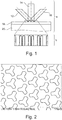
- Fig. 1a schematically shows an exposure to three coplanar beams 12, 14, 16.
- the three beams are distinct and coherent light beams, directed on the same region of a photosensitive resin 18 disposed on a substrate 20, at angles of different incidence.
- the three beams will interfere to form an interference pattern.
- the interference figure achieves a sort of masking of the resin 18, since it comprises areas of varying light intensity, resulting in areas exposed or not exposed to the resin.
- the interference figure allows spatially selective insolation of the resin 18, inducing a corresponding pattern therein.
- the Fig. 1b shows the insolation profile obtained in resin 18 after a single interference exposure to three coplanar beams whose relative intensities are different (here the intensity of the central beam represents half that of the lateral beams).
- the intensity of the central beam represents half that of the lateral beams.
- different patterns with limited symmetry can be obtained by modifying the exposure parameters, including: relative phase shifts between beams, relative intensities between beams, angles of incidence of the beams, exposure time, angle of rotation .
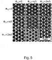
- the figure 5 shows a simulation of the different patterns with limited symmetry that can be obtained by varying the relative phases between the beams 12 and 14 (phase difference noted ⁇ 12 ) and the beams 14 and 16 noted (phase difference noted ⁇ 23 ).
- Steps 1, 3 and 4 are conventional and will therefore not be explained in detail (except in the context of an example below). They can be implemented with existing materials and devices.
- a substrate 44 On a sample holder 42, a substrate 44 has been placed, the upper surface 46 of which is covered with a film of photosensitive resin 48.
- the substrate 44 is for example made of silicon, but may be of any suitable material.
- the photosensitive resin 48 can also be of any suitable type, which will in particular be chosen as a function of the wavelength of the incident beams and of the desired resolution.
- a positive resin with a threshold for example of type S1813
- the type of resin is adapted to the wavelength which is used for its exposure.
- Reference sign 50 denotes a laser source having a predetermined wavelength.
- the coherent light beam 52 produced by the source is first extended through a pair of lenses 54, before meeting a phase mask 56.
- the idea is to widen the source beam 52 so that it extends. over a large area of the mask, for example to reach a diameter of the order of 1 cm.
- the phase mask 56 serves to divide the source beam 52 into three beams of coplanar wave vectors 58.1, 58.2 and 58.3.
- the beam 58.2 is called “central” and the beams 58.1 and 58.2 are called “lateral” or “outer”.
- the phase mask 56 can be a conventional diffraction grating and a commercial phase mask can be used.
- a phase mask from the company IBSEN, having a size of 1 cm x 1 cm and a period of 490 nm designed for S-polarized light. With such a mask, the intensity of the central beam is equal to half of the other two.
- Each beam 58.1, 58.2 and 58.3 is advantageously spatially filtered by passing first through a lens 60 then an orifice 62 (pinhole), which allows a homogeneous distribution of intensity.
- a lens with a focal length of 7.5 cm and an orifice of 5 ⁇ m can be used.
- phase mask can be replaced by any device capable of separating the coherent light source into three beams of coplanar wave vectors.
- a diffraction grating could be used alternatively.
- the central beam 58.2 exits the phase mask 56 perpendicularly thereto, and therefore has a normal incidence on the upper face of the resin 48.
- Two mirrors 64 are used to make the lateral beams 58.1 and 58.3 converge towards the zone of. incidence of the central beam, so that the three beams interfere on the same part of the so-called “exposure surface” resin.
- the respective angles of incidence of the three beams 58.1, 58.2 and 58.3 are denoted ⁇ 1 , ⁇ 0 and ⁇ 2 .
- the angle ⁇ 0 between the central beam F2 and the upper surface of the resin is equal to 90 °.
- the angles ⁇ 1 and ⁇ 2 (angle with respect to the central beam F2) are generally between 5 and 70 °, in particular of the order of 20 °.
- the meeting of the three beams 58.1, 58.2 and 58.3 at the level of the exposure surface will therefore generate an interference pattern, which will make it possible to induce a pattern in the resin film 48.
- the interference comprises zones of varied light intensities, which will, depending on the sensitivity threshold of the resin, generate exposed zones of the resin or non-exposed zones, in accordance with the interference pattern.
- interference lithography is the ability to treat relatively large surfaces by a single exposure step, going with current technical means up to approximately 1 cm 2 , larger surfaces being possible with suitable optics and more powerful lasers.
- the conditions set out above are used to produce three exposures, in particular with a view to obtaining the patterns of stars with three branches. According to variants more exposures can be made, and other symmetrical geometric shapes obtained.
- a first exposure is carried out, referenced as the 0 ° position.
- a first rotation of the sample is carried out, in order to achieve a second exposure - 60 ° position.
- the sample is further rotated by 60 ° in the same direction (therefore by 120 ° with respect to the 0 ° position), in order to carry out a third exposure in the 120 ° position.
- the exposure conditions are the same for all three exposures.
- Rotation of the sample is preferred because it is easier to perform than rotation of the optical system.
- the sample holder is for example mounted on a swivel base 66 comprising a controlled electric motor. It will be noted that the pivoting of the substrate is preferably carried out along an axis of rotation R coincident with the axis F 2 of the central beam 58.2.
- the intensity of the beams it is possible to modulate the relative intensities.
- the outer beams have the same intensity and the intensity of the central beam is reduced, e.g. by 50%.
- phase modulation between the different beams makes it possible to vary the patterns, as seen for example in Fig. 5 .
- a silicon substrate 44 coated on its upper face with a photosensitive resin 48 (for reasons of simplicity, the same reference signs are used as in the figure Fig. 3 ).
- Silicon substrates having a thickness of 600-750 ⁇ m were cleaned for 5 min in an ultrasonic bath of acetone and isopropanol. The substrates were then dried and placed on a hot plate at 400 ° C to improve the adhesion between the silicon and the resin.
- the photosensitive resin chosen was a positive resin with a threshold, in particular an S1813 resin (Microchem company), sensitive to wavelengths of 405 nm and a resolution of 0.5 ⁇ m.
- the resin diluted to 50% in a solvent (Microposit EC) was deposited in a thin layer of 350 nm by means of a spin coater (30 s at 4000 rpm, acceleration 3000 rpm). The solvent was evaporated in an oven at 110 ° C.
- the substrate 44 thus prepared with its thin layer of photosensitive resin 48 was then placed in an optical system of the type of the Fig. 3 (equipped with a 450 nm laser) to undergo an exposure step comprising a triple interference exposure with three coplanar beams, in accordance with the present invention.
- Image a) shows the principle of an interference exposure, in which the three light beams 58.1, 58.2 and 58.3 produced by the optical system converge on the same part of the surface and interfere together.
- Three interference exposures of resin 48 were carried out, for angular positions of the substrate of 0 °, 60 ° and 120 °. Each exposure was carried out under the same conditions for the incident beams (intensity of the central beam is half that of the beams lateral), with a duration of a few tens of seconds, depending on the intensity of the laser beam exposing the sample.
- This exposure step therefore makes it possible to induce the pattern of the interference figure produced by the three coplanar beams, as represented by image b).
- the exposed areas i.e. in which the light intensity of the interference pattern was greater than the sensitivity threshold of the resin.
- the resin is developed to reveal the induced structure. Development was performed in an MF319 developer solution (MicroChem) for 30 s, followed by a water rinse.
- MF319 developer solution MocroChem
- Image d represents the deposition of gold by evaporation. After development of the resin, a 3 nm thick chromium adhesion layer was first preferably formed (not shown). Then a 50 nm layer of gold, designated 74, was deposited by thermal evaporation (at the rate of 1 nm / s).
- the last step aims to remove the sacrificial material, i.e. the resin, remaining on the substrate 44.
- the respective thicknesses of the sacrificial material (resin) and of the target material layer (gold) deposited on the latter will be adjusted, in a conventional manner. Indeed, if the resin thickness is too Importantly, the target material settles on the sides of the cutouts, which protects the underlying resin (image e, left).
- the thickness of resin 48 does not generally exceed three times the thickness of the layer 74 of gold.
- the shading phenomenon prevents the deposition of gold on the sides of the resin profile and therefore leads to a discontinuity of the gold layer (denoted 74.1) between the top of the resin and the gold layer (denoted 74.2) formed in the holes on the substrate 44. It is thus possible to chemically dissolve the resin 48 and thereby remove the metal 74.1 deposited on the latter. In the present example, the resin was dissolved with acetone.
- the upper face 46 of the substrate 44 only bears the desired metal nanostructures 74.2, here the three-branched gold nanostructures.
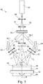
- the figure 6 shows an embodiment of an optical system 100 employing a truncated prism, allowing the implementation of the present method.
- a substrate 44 ' will be recognized, the upper surface 46' of which is covered with a film of photosensitive resin 48 '.
- the reference sign 102 designates a prism having an upper face 102.1 and a lower face 102.2 (or base) which are plane and parallel In the vertical plane of the figure, the prism 102 has a trapezoidal section: the base 102.2 is therefore wider than the upper face 102.1 and there are two opposite and symmetrical side faces 102.3 which join the two faces 102.1 and 102.2.
- a prism can typically be a right prism, in particular a Dove prism, which has been placed on a lateral face.
- the prism is in a transparent material in the light, typically in flint or crown glass for the visible or quartz in the UV.
- the coplanar light beams are generally indicated 104 and are directed, upstream of the prism, perpendicularly. on the resin surface.
- the central part of the beams attacks the planar upper surface 102.1 (parallel to its base 102.2 and to the upper resin surface) of the prism 102, passes through the latter and reaches the region of the resin surface with an angle of incidence of 90 °. This therefore forms the central beam F2.
- the coplanar beams 104 arrive on the inclined side faces of the prism 102.3 undergo a deviation (refraction) during their penetration into the prism, and arrive at the region of the resin surface with a angle of incidence different from 90 °.
- the lateral beams F1 and F3 are thus formed.
- phase and the intensity can advantageously be controlled by optical layers arranged on the side faces or at a distance.
- the phase of the side beams is controlled by means of thin optical layers 108 formed on the opposing side faces 102.3 of the prism.
- Optical density are positioned on the path of the end light beams, upstream of the prism, vertically to the side faces 102.3.
- Optical densities are generally absorbent layers, which may have a thickness of the order of a few nanometers in the case of metals or even a few tens of nanometers or even hundreds of nanometers if produced using doped oxides.
- these optical densities could be formed as thin layers directly on the side surfaces of the prism, e.g. above phase control layers 108.
- the prism 102 provides three coplanar beams which meet and interfere in the region of the base of the prism (indicated by dotted lines), near the surface of the resin 48 '. It is thus possible to insulate the resin 48 'by interference figures, in a manner similar to the optical system of the figure 3 .
- the use of the prism 102 in the optical system 100 allows great compactness. At the same time, it ensures the separation of the beams and their orientation, directing the lateral beams to make them interfere in the region of its base 102.2.
- the prism 102 can be placed directly on the photosensitive resin layer 48 '. It could also be slightly spaced. It will also be noted that with a transparent substrate of low thickness, the base of the prism can be placed against the rear face of the substrate (opposite to the face bearing the resin), in order to insulate the resin through the substrate. This is then an interference insolation by transmission.
Landscapes
- Physics & Mathematics (AREA)
- General Physics & Mathematics (AREA)
- Engineering & Computer Science (AREA)
- Signal Processing (AREA)
- Exposure And Positioning Against Photoresist Photosensitive Materials (AREA)
Claims (12)
- Verfahren zur Herstellung von Strukturen mit begrenzter Symmetrie durch Interferenzlithographie, das einen Schritt zur Belichtung mithilfe der Interferenzlithographie eines lichtempfindlichen Materials (18) umfasst, das auf einem Substrat (20) angeordnet ist;
dadurch gekennzeichnet, dass der Schritt zur Belichtung mindestens drei aufeinanderfolgende Interferenzbelichtungen umfasst, die mit drei koplanaren Lichtstrahlenbündeln (12, 14, 16) ausgeführt werden, die von einem optischen System stammen und auf einer Belichtungsfläche des lichtempfindlichen Materials interferieren; wobei eine erste relative Drehung zwischen dem optischen System und dem Substrat zwischen der ersten und der zweiten Interferenzbelichtung und dann eine zweite Drehung zwischen der zweiten und der dritten Interferenzbelichtung erfolgt. - Verfahren nach Anspruch 1, wobei die relativen Intensitäten der koplanaren Strahlenbündel gesteuert werden.
- Verfahren nach Anspruch 2, wobei ein mittiges Strahlenbündel eine Intensität aufweist, die gleich der Hälfte von der der äußeren Strahlenbündel ist.
- Verfahren nach Anspruch 1, 2 oder 3, wobei die jeweiligen Phasen der Lichtstrahlenbündel moduliert werden; und vorzugsweise die jeweiligen Phasen der Strahlenbündel gesteuert werden.
- Verfahren nach einem der vorangehenden Ansprüche, wobei die drei koplanaren Lichtstrahlenbündel von einem optischen System emittiert werden, das Folgendes erzeugt: ein mittiges Strahlenbündel, vorzugsweise mit einem zur Substratebene normalen Einfallswinkel, und zwei seitliche Strahlenbündel an den beiden Seiten des mittigen Strahlenbündels und in der gleichen Ebene, wobei die seitlichen Strahlenbündel einen Einfallswinkel von kleiner als 90 Grad zur Substratebene aufweisen und die drei Lichtstrahlenbündel im Wesentlichen auf die Belichtungsfläche des lichtempfindlichen Materials geleitet werden, um ein Interferenzbild zu erzeugen.
- Verfahren nach Anspruch 5, wobei der Einfallswinkel der seitlichen Strahlenbündel (in Bezug auf die Flächennormale) im Bereich von 5° und 70° liegt.
- Verfahren nach einem der vorangehenden Ansprüche, wobei die drei Belichtungen unter den Winkeln von 0°, 60° und 120° erfolgen; und wobei die relative Drehbewegung für das Substrat vorzugsweise durch Ortsänderung des Substrats erfolgt.
- Verfahren nach einem der vorangehenden Ansprüche, wobei das optische System ein Strahlenbündel-Bildungsmittel umfasst, das am Eingang ein von einer kohärenten Lichtquelle erzeugtes Lichtstrahlenbündel erhält und drei koplanare Lichtstrahlenbündel erzeugen kann.
- Verfahren nach einem der vorangehenden Ansprüche, das außerdem Folgendes umfasst:einen Schritt zur Entwicklung des lichtempfindlichen Materials, um selektiv vordefinierte Regionen der Belichtungsfläche freizugeben, im Anschluss an den Schritt der Belichtung; undeinen Schritt zur Herstellung der Struktur gemäß der Maske, die vom entwickelten lichtempfindlichen Material gebildet wurde.
- Verfahren nach Anspruch 9, bei dem der Schritt zur Herstellung das Aufbringen von Material, insbesondere durch Metallaufdampfung, durch die Maske hindurch und die anschließende Auflösung des lichtempfindlichen Materials umfasst.
- Verfahren nach einem der vorangehenden Ansprüche, wobei die auf dem Substrat hergestellte Struktur Nanoteilchen oder Gruppen von Nanoteilchen umfasst, die eine Form oder eine Anordnung mit einer Symmetrieachse senkrecht zu einer Fläche vom Typ Cn aufweisen, wobei n größer als oder gleich drei ist; und wobei die Nanoteilchen metallisch und/oder halbleitend sind und/oder die Nanoteilchen eine Abmessung aufweisen, die im Bereich eines Nanometers oder mehrerer zehn Mikrometer liegt und/oder die Nanoteilchen mindestens auf einem Teil des Substrats gemäß einem regelmäßigen oder quasikristallinen Muster angeordnet sind, und zwar in Abhängigkeit des Netzes, in dem Nanoteilchen eingeschlossen sind.
- Optisches System für die Herstellung von Strukturen mit begrenzter Symmetrie durch Interferenzlithographie, umfassend:einen Probenhalter;eine kohärente Lichtquelle, die ein Ausgangslichtstrahlenbündel emittiert;Mittel für das Bilden aus dem Ausgangslichtstrahlenbündel von drei koplanaren Lichtstrahlenbündeln (F1, F2, F3), die auf eine Belichtungsfläche eines lichtempfindlichen Harzes (48'), das ein Substrat (44') bedeckt, geleitet werden, um zu interferieren;Mittel zum Drehen des Probenhalters, um für das Harz mehrere Interferenzbelichtungen auszuführen;wobei die Mittel zum Bilden des Strahlenbündels Folgendes umfassen:ein Prisma (102), das eine untere Fläche (102.2) und eine obere Fläche (102.1), die eben und parallel sind, und zwei seitliche Flächen (102.3) aufweist, die entgegengesetzt schräg sind, wobei bei der Anwendung die untere Fläche des Primas in der Nähe des Substrats oder in Kontakt mit dem Substrat, das mit der lichtempfindlichen Harzschicht bedeckt ist, angeordnet wird, während das Ausgangslichtstrahlenbündel senkrecht zur unteren Fläche des Prismas geleitet wird und auf die obere Fläche des Prismas sowie auf die zwei schrägen seitlichen Flächen fällt;dadurch gekennzeichnet, dass das Prisma so konfiguriert ist, dass die durch die obere Fläche eindringenden Strahlenbündel unter einem normalen Einfall auf die untere Fläche des Prismas gelangen und die durch die seitlichen Flächen eindringenden Lichtstrahlenbündel zum Interferieren zur unteren Fläche hin konvergieren;dass eine Dickenanpassungsschicht (108) optional auf jeder der schrägen seitlichen Flächen des Prismas angeordnet ist, um die Phase der Lichtstrahlenbündel zu steuern; unddass eine optische Dichte (110) entweder angeordnet ist auf dem Weg der Lichtstrahlenbündel (F1, F3), die auf die schrägen seitlichen Flächen fallen, oder auf dem Weg der Lichtstrahlenbündel, die auf die obere Fläche des Prismas fallen, um deren Intensität abzuschwächen, wobei die optische Dichte die Form eines vom Prisma entfernt angeordneten Plättchens oder einer auf dem Prisma gebildeten Schicht, beziehungsweise auf der Dickenanpassungsschicht, annehmen kann.
Applications Claiming Priority (2)
| Application Number | Priority Date | Filing Date | Title |
|---|---|---|---|
| FR1756863A FR3069341B1 (fr) | 2017-07-19 | 2017-07-19 | Procede de lithographie interferentielle |
| PCT/EP2018/068793 WO2019016045A1 (fr) | 2017-07-19 | 2018-07-11 | Procédé de lithographie interférentielle |
Publications (2)
| Publication Number | Publication Date |
|---|---|
| EP3655821A1 EP3655821A1 (de) | 2020-05-27 |
| EP3655821B1 true EP3655821B1 (de) | 2021-07-14 |
Family
ID=60382314
Family Applications (1)
| Application Number | Title | Priority Date | Filing Date |
|---|---|---|---|
| EP18737918.5A Active EP3655821B1 (de) | 2017-07-19 | 2018-07-11 | Interferenzlithographie -verfahren und -system |
Country Status (3)
| Country | Link |
|---|---|
| EP (1) | EP3655821B1 (de) |
| FR (1) | FR3069341B1 (de) |
| WO (1) | WO2019016045A1 (de) |
Families Citing this family (1)
| Publication number | Priority date | Publication date | Assignee | Title |
|---|---|---|---|---|
| CN112099121B (zh) * | 2020-09-29 | 2022-07-22 | 北京华卓精科科技股份有限公司 | 基于4f系统的扫描干涉光刻系统 |
Family Cites Families (2)
| Publication number | Priority date | Publication date | Assignee | Title |
|---|---|---|---|---|
| US5759744A (en) * | 1995-02-24 | 1998-06-02 | University Of New Mexico | Methods and apparatus for lithography of sparse arrays of sub-micrometer features |
| FR2964469B1 (fr) | 2010-09-08 | 2016-01-01 | Univ Troyes Technologie | Substrat revetu de nanoparticules, et son utilisation pour la detection de molecules isolees. |
-
2017
- 2017-07-19 FR FR1756863A patent/FR3069341B1/fr not_active Expired - Fee Related
-
2018
- 2018-07-11 WO PCT/EP2018/068793 patent/WO2019016045A1/fr not_active Ceased
- 2018-07-11 EP EP18737918.5A patent/EP3655821B1/de active Active
Also Published As
| Publication number | Publication date |
|---|---|
| EP3655821A1 (de) | 2020-05-27 |
| FR3069341A1 (fr) | 2019-01-25 |
| FR3069341B1 (fr) | 2022-11-11 |
| WO2019016045A1 (fr) | 2019-01-24 |
Similar Documents
| Publication | Publication Date | Title |
|---|---|---|
| US8427639B2 (en) | Surfaced enhanced Raman spectroscopy substrates | |
| EP2616855B1 (de) | Spektralbandpassfilter mit hoher selektivität und gesteuerter polarisation | |
| US9726788B2 (en) | Method for fabricating nanoantenna array, nanoantenna array chip and structure for lithography | |
| US8358407B2 (en) | Enhancing signals in Surface Enhanced Raman Spectroscopy (SERS) | |
| Braun et al. | Versatile direct laser writing lithography technique for surface enhanced infrared spectroscopy sensors | |
| EP1652009B1 (de) | Verfahren zur herstellung von mustern mit geneigten flanken mittels fotolithographie | |
| EP3924757B1 (de) | Optische metaoberflächen und zugehörige herstellungsverfahren und -systeme | |
| FR2547111A1 (fr) | Procede de correction de masques lithographiques | |
| EP3040710B1 (de) | Herstellungsverfahren eines substrats zur verstärkten raman-streuung an der oberfläche | |
| EP4381349A1 (de) | Verfahren zur herstellung einer uhrkomponente | |
| Wang et al. | Fabrication of silver-silicon gratings for surface plasmon excitation using nanosecond laser interference lithography | |
| EP3655821B1 (de) | Interferenzlithographie -verfahren und -system | |
| EP2616235A1 (de) | Verfahren zur herstellung einer segmentierten optischen struktur | |
| KR102272003B1 (ko) | 기판 상의 패턴 형성방법 및 이에 따라 제조되는 패턴이 형성된 기판 | |
| FR2798739A1 (fr) | Masque a dephasage utilisant le cra1on comme materiau de dephasage et procede de fabrication de celui-ci | |
| EP3040711B1 (de) | Herstellungsverfahren eines substrats zur oberflächenverstärkten raman-streuung, und entsprechendes substrat | |
| FR3062516A1 (fr) | Procede de mesure du desalignement entre une premiere et une seconde zones de gravure | |
| FR2733854A1 (fr) | Dispositif de focalisation/dispersion de rayons x et procede de production de celui-ci | |
| EP3472669B1 (de) | System und verfahren zur herstellung einer maske für die oberflächenmikrotexturierung sowie anlage und verfahren zur oberflächenmikrotexturierung | |
| Qu et al. | Mask-based microsphere photolithography | |
| Cardoso | Development of resonant nanostructures large area device for augmented reality | |
| JP2026049448A (ja) | 電場増強素子およびラマン分光装置 | |
| Dvoretckaia et al. | High resolution photolithography using arrays of polystyrene and SiO2 micro-and nano-sized spherical lenses | |
| EP3472668B1 (de) | System und verfahren zur herstellung einer optischen maske zur oberflächenbehandlung sowie oberflächenbehandlungsanlage und verfahren | |
| JP2026049260A (ja) | 電場増強素子およびラマン分光装置 |
Legal Events
| Date | Code | Title | Description |
|---|---|---|---|
| STAA | Information on the status of an ep patent application or granted ep patent |
Free format text: STATUS: UNKNOWN |
|
| STAA | Information on the status of an ep patent application or granted ep patent |
Free format text: STATUS: THE INTERNATIONAL PUBLICATION HAS BEEN MADE |
|
| PUAI | Public reference made under article 153(3) epc to a published international application that has entered the european phase |
Free format text: ORIGINAL CODE: 0009012 |
|
| STAA | Information on the status of an ep patent application or granted ep patent |
Free format text: STATUS: REQUEST FOR EXAMINATION WAS MADE |
|
| 17P | Request for examination filed |
Effective date: 20200212 |
|
| AK | Designated contracting states |
Kind code of ref document: A1 Designated state(s): AL AT BE BG CH CY CZ DE DK EE ES FI FR GB GR HR HU IE IS IT LI LT LU LV MC MK MT NL NO PL PT RO RS SE SI SK SM TR |
|
| AX | Request for extension of the european patent |
Extension state: BA ME |
|
| DAV | Request for validation of the european patent (deleted) | ||
| DAX | Request for extension of the european patent (deleted) | ||
| REG | Reference to a national code |
Ref country code: DE Ref legal event code: R079 Ref document number: 602018020127 Country of ref document: DE Free format text: PREVIOUS MAIN CLASS: G03F0007200000 Ipc: G03F0009000000 |
|
| GRAP | Despatch of communication of intention to grant a patent |
Free format text: ORIGINAL CODE: EPIDOSNIGR1 |
|
| STAA | Information on the status of an ep patent application or granted ep patent |
Free format text: STATUS: GRANT OF PATENT IS INTENDED |
|
| RIC1 | Information provided on ipc code assigned before grant |
Ipc: G03F 9/00 20060101AFI20210324BHEP |
|
| INTG | Intention to grant announced |
Effective date: 20210415 |
|
| GRAS | Grant fee paid |
Free format text: ORIGINAL CODE: EPIDOSNIGR3 |
|
| GRAA | (expected) grant |
Free format text: ORIGINAL CODE: 0009210 |
|
| STAA | Information on the status of an ep patent application or granted ep patent |
Free format text: STATUS: THE PATENT HAS BEEN GRANTED |
|
| AK | Designated contracting states |
Kind code of ref document: B1 Designated state(s): AL AT BE BG CH CY CZ DE DK EE ES FI FR GB GR HR HU IE IS IT LI LT LU LV MC MK MT NL NO PL PT RO RS SE SI SK SM TR |
|
| REG | Reference to a national code |
Ref country code: GB Ref legal event code: FG4D Free format text: NOT ENGLISH |
|
| REG | Reference to a national code |
Ref country code: IE Ref legal event code: FG4D Free format text: LANGUAGE OF EP DOCUMENT: FRENCH |
|
| REG | Reference to a national code |
Ref country code: DE Ref legal event code: R096 Ref document number: 602018020127 Country of ref document: DE |
|
| REG | Reference to a national code |
Ref country code: AT Ref legal event code: REF Ref document number: 1411131 Country of ref document: AT Kind code of ref document: T Effective date: 20210815 |
|
| REG | Reference to a national code |
Ref country code: LT Ref legal event code: MG9D |
|
| REG | Reference to a national code |
Ref country code: NL Ref legal event code: MP Effective date: 20210714 |
|
| REG | Reference to a national code |
Ref country code: AT Ref legal event code: MK05 Ref document number: 1411131 Country of ref document: AT Kind code of ref document: T Effective date: 20210714 |
|
| PG25 | Lapsed in a contracting state [announced via postgrant information from national office to epo] |
Ref country code: RS Free format text: LAPSE BECAUSE OF FAILURE TO SUBMIT A TRANSLATION OF THE DESCRIPTION OR TO PAY THE FEE WITHIN THE PRESCRIBED TIME-LIMIT Effective date: 20210714 Ref country code: SE Free format text: LAPSE BECAUSE OF FAILURE TO SUBMIT A TRANSLATION OF THE DESCRIPTION OR TO PAY THE FEE WITHIN THE PRESCRIBED TIME-LIMIT Effective date: 20210714 Ref country code: HR Free format text: LAPSE BECAUSE OF FAILURE TO SUBMIT A TRANSLATION OF THE DESCRIPTION OR TO PAY THE FEE WITHIN THE PRESCRIBED TIME-LIMIT Effective date: 20210714 Ref country code: ES Free format text: LAPSE BECAUSE OF FAILURE TO SUBMIT A TRANSLATION OF THE DESCRIPTION OR TO PAY THE FEE WITHIN THE PRESCRIBED TIME-LIMIT Effective date: 20210714 Ref country code: FI Free format text: LAPSE BECAUSE OF FAILURE TO SUBMIT A TRANSLATION OF THE DESCRIPTION OR TO PAY THE FEE WITHIN THE PRESCRIBED TIME-LIMIT Effective date: 20210714 Ref country code: LT Free format text: LAPSE BECAUSE OF FAILURE TO SUBMIT A TRANSLATION OF THE DESCRIPTION OR TO PAY THE FEE WITHIN THE PRESCRIBED TIME-LIMIT Effective date: 20210714 Ref country code: BG Free format text: LAPSE BECAUSE OF FAILURE TO SUBMIT A TRANSLATION OF THE DESCRIPTION OR TO PAY THE FEE WITHIN THE PRESCRIBED TIME-LIMIT Effective date: 20211014 Ref country code: AT Free format text: LAPSE BECAUSE OF FAILURE TO SUBMIT A TRANSLATION OF THE DESCRIPTION OR TO PAY THE FEE WITHIN THE PRESCRIBED TIME-LIMIT Effective date: 20210714 Ref country code: NL Free format text: LAPSE BECAUSE OF FAILURE TO SUBMIT A TRANSLATION OF THE DESCRIPTION OR TO PAY THE FEE WITHIN THE PRESCRIBED TIME-LIMIT Effective date: 20210714 Ref country code: NO Free format text: LAPSE BECAUSE OF FAILURE TO SUBMIT A TRANSLATION OF THE DESCRIPTION OR TO PAY THE FEE WITHIN THE PRESCRIBED TIME-LIMIT Effective date: 20211014 Ref country code: PT Free format text: LAPSE BECAUSE OF FAILURE TO SUBMIT A TRANSLATION OF THE DESCRIPTION OR TO PAY THE FEE WITHIN THE PRESCRIBED TIME-LIMIT Effective date: 20211115 |
|
| PG25 | Lapsed in a contracting state [announced via postgrant information from national office to epo] |
Ref country code: PL Free format text: LAPSE BECAUSE OF FAILURE TO SUBMIT A TRANSLATION OF THE DESCRIPTION OR TO PAY THE FEE WITHIN THE PRESCRIBED TIME-LIMIT Effective date: 20210714 Ref country code: LV Free format text: LAPSE BECAUSE OF FAILURE TO SUBMIT A TRANSLATION OF THE DESCRIPTION OR TO PAY THE FEE WITHIN THE PRESCRIBED TIME-LIMIT Effective date: 20210714 Ref country code: GR Free format text: LAPSE BECAUSE OF FAILURE TO SUBMIT A TRANSLATION OF THE DESCRIPTION OR TO PAY THE FEE WITHIN THE PRESCRIBED TIME-LIMIT Effective date: 20211015 |
|
| REG | Reference to a national code |
Ref country code: DE Ref legal event code: R097 Ref document number: 602018020127 Country of ref document: DE |
|
| PG25 | Lapsed in a contracting state [announced via postgrant information from national office to epo] |
Ref country code: DK Free format text: LAPSE BECAUSE OF FAILURE TO SUBMIT A TRANSLATION OF THE DESCRIPTION OR TO PAY THE FEE WITHIN THE PRESCRIBED TIME-LIMIT Effective date: 20210714 |
|
| PLBE | No opposition filed within time limit |
Free format text: ORIGINAL CODE: 0009261 |
|
| STAA | Information on the status of an ep patent application or granted ep patent |
Free format text: STATUS: NO OPPOSITION FILED WITHIN TIME LIMIT |
|
| PG25 | Lapsed in a contracting state [announced via postgrant information from national office to epo] |
Ref country code: SM Free format text: LAPSE BECAUSE OF FAILURE TO SUBMIT A TRANSLATION OF THE DESCRIPTION OR TO PAY THE FEE WITHIN THE PRESCRIBED TIME-LIMIT Effective date: 20210714 Ref country code: SK Free format text: LAPSE BECAUSE OF FAILURE TO SUBMIT A TRANSLATION OF THE DESCRIPTION OR TO PAY THE FEE WITHIN THE PRESCRIBED TIME-LIMIT Effective date: 20210714 Ref country code: RO Free format text: LAPSE BECAUSE OF FAILURE TO SUBMIT A TRANSLATION OF THE DESCRIPTION OR TO PAY THE FEE WITHIN THE PRESCRIBED TIME-LIMIT Effective date: 20210714 Ref country code: EE Free format text: LAPSE BECAUSE OF FAILURE TO SUBMIT A TRANSLATION OF THE DESCRIPTION OR TO PAY THE FEE WITHIN THE PRESCRIBED TIME-LIMIT Effective date: 20210714 Ref country code: CZ Free format text: LAPSE BECAUSE OF FAILURE TO SUBMIT A TRANSLATION OF THE DESCRIPTION OR TO PAY THE FEE WITHIN THE PRESCRIBED TIME-LIMIT Effective date: 20210714 Ref country code: AL Free format text: LAPSE BECAUSE OF FAILURE TO SUBMIT A TRANSLATION OF THE DESCRIPTION OR TO PAY THE FEE WITHIN THE PRESCRIBED TIME-LIMIT Effective date: 20210714 |
|
| 26N | No opposition filed |
Effective date: 20220419 |
|
| PG25 | Lapsed in a contracting state [announced via postgrant information from national office to epo] |
Ref country code: MC Free format text: LAPSE BECAUSE OF FAILURE TO SUBMIT A TRANSLATION OF THE DESCRIPTION OR TO PAY THE FEE WITHIN THE PRESCRIBED TIME-LIMIT Effective date: 20210714 |
|
| REG | Reference to a national code |
Ref country code: CH Ref legal event code: PL |
|
| REG | Reference to a national code |
Ref country code: BE Ref legal event code: MM Effective date: 20220731 |
|
| PG25 | Lapsed in a contracting state [announced via postgrant information from national office to epo] |
Ref country code: LU Free format text: LAPSE BECAUSE OF NON-PAYMENT OF DUE FEES Effective date: 20220711 Ref country code: LI Free format text: LAPSE BECAUSE OF NON-PAYMENT OF DUE FEES Effective date: 20220731 Ref country code: CH Free format text: LAPSE BECAUSE OF NON-PAYMENT OF DUE FEES Effective date: 20220731 |
|
| PG25 | Lapsed in a contracting state [announced via postgrant information from national office to epo] |
Ref country code: BE Free format text: LAPSE BECAUSE OF NON-PAYMENT OF DUE FEES Effective date: 20220731 |
|
| PG25 | Lapsed in a contracting state [announced via postgrant information from national office to epo] |
Ref country code: IE Free format text: LAPSE BECAUSE OF NON-PAYMENT OF DUE FEES Effective date: 20220711 |
|
| PG25 | Lapsed in a contracting state [announced via postgrant information from national office to epo] |
Ref country code: MK Free format text: LAPSE BECAUSE OF FAILURE TO SUBMIT A TRANSLATION OF THE DESCRIPTION OR TO PAY THE FEE WITHIN THE PRESCRIBED TIME-LIMIT Effective date: 20210714 Ref country code: CY Free format text: LAPSE BECAUSE OF FAILURE TO SUBMIT A TRANSLATION OF THE DESCRIPTION OR TO PAY THE FEE WITHIN THE PRESCRIBED TIME-LIMIT Effective date: 20210714 |
|
| PG25 | Lapsed in a contracting state [announced via postgrant information from national office to epo] |
Ref country code: HU Free format text: LAPSE BECAUSE OF FAILURE TO SUBMIT A TRANSLATION OF THE DESCRIPTION OR TO PAY THE FEE WITHIN THE PRESCRIBED TIME-LIMIT; INVALID AB INITIO Effective date: 20180711 |
|
| PG25 | Lapsed in a contracting state [announced via postgrant information from national office to epo] |
Ref country code: TR Free format text: LAPSE BECAUSE OF FAILURE TO SUBMIT A TRANSLATION OF THE DESCRIPTION OR TO PAY THE FEE WITHIN THE PRESCRIBED TIME-LIMIT Effective date: 20210714 |
|
| PG25 | Lapsed in a contracting state [announced via postgrant information from national office to epo] |
Ref country code: MT Free format text: LAPSE BECAUSE OF FAILURE TO SUBMIT A TRANSLATION OF THE DESCRIPTION OR TO PAY THE FEE WITHIN THE PRESCRIBED TIME-LIMIT Effective date: 20210714 |
|
| PGFP | Annual fee paid to national office [announced via postgrant information from national office to epo] |
Ref country code: DE Payment date: 20240719 Year of fee payment: 7 |
|
| PGFP | Annual fee paid to national office [announced via postgrant information from national office to epo] |
Ref country code: GB Payment date: 20240722 Year of fee payment: 7 |
|
| PGFP | Annual fee paid to national office [announced via postgrant information from national office to epo] |
Ref country code: FR Payment date: 20240723 Year of fee payment: 7 |
|
| PGFP | Annual fee paid to national office [announced via postgrant information from national office to epo] |
Ref country code: IT Payment date: 20240731 Year of fee payment: 7 |
|
| REG | Reference to a national code |
Ref country code: DE Ref legal event code: R119 Ref document number: 602018020127 Country of ref document: DE |
|
| GBPC | Gb: european patent ceased through non-payment of renewal fee |
Effective date: 20250711 |
|
| PG25 | Lapsed in a contracting state [announced via postgrant information from national office to epo] |
Ref country code: GB Free format text: LAPSE BECAUSE OF NON-PAYMENT OF DUE FEES Effective date: 20250711 |
|
| PG25 | Lapsed in a contracting state [announced via postgrant information from national office to epo] |
Ref country code: DE Free format text: LAPSE BECAUSE OF NON-PAYMENT OF DUE FEES Effective date: 20260203 |
|
| PG25 | Lapsed in a contracting state [announced via postgrant information from national office to epo] |
Ref country code: FR Free format text: LAPSE BECAUSE OF NON-PAYMENT OF DUE FEES Effective date: 20250731 |