EP1677158A2 - Verfahrung zur Messung von Substratinformationen und Substrat für Gebrauch in einem lithografischen Apparat - Google Patents
Verfahrung zur Messung von Substratinformationen und Substrat für Gebrauch in einem lithografischen Apparat Download PDFInfo
- Publication number
- EP1677158A2 EP1677158A2 EP05258013A EP05258013A EP1677158A2 EP 1677158 A2 EP1677158 A2 EP 1677158A2 EP 05258013 A EP05258013 A EP 05258013A EP 05258013 A EP05258013 A EP 05258013A EP 1677158 A2 EP1677158 A2 EP 1677158A2
- Authority
- EP
- European Patent Office
- Prior art keywords
- substrate
- marker
- feature
- coating
- information
- Prior art date
- Legal status (The legal status is an assumption and is not a legal conclusion. Google has not performed a legal analysis and makes no representation as to the accuracy of the status listed.)
- Withdrawn
Links
- 239000000758 substrate Substances 0.000 title claims abstract description 148
- 238000000034 method Methods 0.000 title claims abstract description 50
- 239000003550 marker Substances 0.000 claims abstract description 85
- 238000000576 coating method Methods 0.000 claims abstract description 33
- 239000011248 coating agent Substances 0.000 claims abstract description 32
- 238000000059 patterning Methods 0.000 claims description 36
- 229910052751 metal Inorganic materials 0.000 claims description 14
- 239000002184 metal Substances 0.000 claims description 14
- 230000003287 optical effect Effects 0.000 claims description 11
- 239000006117 anti-reflective coating Substances 0.000 claims description 8
- 238000004519 manufacturing process Methods 0.000 claims description 7
- 239000004411 aluminium Substances 0.000 claims description 6
- 229910052782 aluminium Inorganic materials 0.000 claims description 6
- XAGFODPZIPBFFR-UHFFFAOYSA-N aluminium Chemical compound [Al] XAGFODPZIPBFFR-UHFFFAOYSA-N 0.000 claims description 6
- 239000000463 material Substances 0.000 claims description 5
- 230000003667 anti-reflective effect Effects 0.000 claims description 4
- 238000012360 testing method Methods 0.000 claims description 4
- 239000013078 crystal Substances 0.000 claims description 3
- 229910052715 tantalum Inorganic materials 0.000 claims description 3
- GUVRBAGPIYLISA-UHFFFAOYSA-N tantalum atom Chemical compound [Ta] GUVRBAGPIYLISA-UHFFFAOYSA-N 0.000 claims description 3
- 230000003252 repetitive effect Effects 0.000 claims 1
- 230000005855 radiation Effects 0.000 description 31
- 239000010410 layer Substances 0.000 description 20
- 238000005259 measurement Methods 0.000 description 7
- 238000001514 detection method Methods 0.000 description 6
- 238000009826 distribution Methods 0.000 description 4
- 238000001459 lithography Methods 0.000 description 4
- 238000005286 illumination Methods 0.000 description 3
- 238000007654 immersion Methods 0.000 description 3
- 230000033001 locomotion Effects 0.000 description 3
- 239000005022 packaging material Substances 0.000 description 3
- 230000008569 process Effects 0.000 description 3
- 230000001419 dependent effect Effects 0.000 description 2
- 238000003384 imaging method Methods 0.000 description 2
- 238000007689 inspection Methods 0.000 description 2
- 239000007788 liquid Substances 0.000 description 2
- 238000013507 mapping Methods 0.000 description 2
- 150000002739 metals Chemical class 0.000 description 2
- 230000010363 phase shift Effects 0.000 description 2
- 210000001747 pupil Anatomy 0.000 description 2
- 239000004065 semiconductor Substances 0.000 description 2
- 230000003068 static effect Effects 0.000 description 2
- 238000012876 topography Methods 0.000 description 2
- 238000001429 visible spectrum Methods 0.000 description 2
- XUIMIQQOPSSXEZ-UHFFFAOYSA-N Silicon Chemical compound [Si] XUIMIQQOPSSXEZ-UHFFFAOYSA-N 0.000 description 1
- 238000003491 array Methods 0.000 description 1
- 230000002238 attenuated effect Effects 0.000 description 1
- 230000008901 benefit Effects 0.000 description 1
- 230000008033 biological extinction Effects 0.000 description 1
- 230000008859 change Effects 0.000 description 1
- 238000004590 computer program Methods 0.000 description 1
- 230000001143 conditioned effect Effects 0.000 description 1
- 230000003750 conditioning effect Effects 0.000 description 1
- 238000013500 data storage Methods 0.000 description 1
- 230000001066 destructive effect Effects 0.000 description 1
- 238000011161 development Methods 0.000 description 1
- 230000009977 dual effect Effects 0.000 description 1
- 230000005670 electromagnetic radiation Effects 0.000 description 1
- 238000010894 electron beam technology Methods 0.000 description 1
- 238000005530 etching Methods 0.000 description 1
- 239000012530 fluid Substances 0.000 description 1
- 230000003993 interaction Effects 0.000 description 1
- 238000005468 ion implantation Methods 0.000 description 1
- 238000010884 ion-beam technique Methods 0.000 description 1
- 239000002346 layers by function Substances 0.000 description 1
- 239000004973 liquid crystal related substance Substances 0.000 description 1
- 230000005381 magnetic domain Effects 0.000 description 1
- 239000011159 matrix material Substances 0.000 description 1
- 230000015654 memory Effects 0.000 description 1
- QSHDDOUJBYECFT-UHFFFAOYSA-N mercury Chemical compound [Hg] QSHDDOUJBYECFT-UHFFFAOYSA-N 0.000 description 1
- 229910052753 mercury Inorganic materials 0.000 description 1
- 238000001465 metallisation Methods 0.000 description 1
- 238000012986 modification Methods 0.000 description 1
- 230000004048 modification Effects 0.000 description 1
- 230000003647 oxidation Effects 0.000 description 1
- 238000007254 oxidation reaction Methods 0.000 description 1
- 239000002245 particle Substances 0.000 description 1
- 230000000737 periodic effect Effects 0.000 description 1
- 238000005498 polishing Methods 0.000 description 1
- 230000037452 priming Effects 0.000 description 1
- 238000012545 processing Methods 0.000 description 1
- 230000004044 response Effects 0.000 description 1
- 238000007493 shaping process Methods 0.000 description 1
- 229910052710 silicon Inorganic materials 0.000 description 1
- 239000010703 silicon Substances 0.000 description 1
- 238000001228 spectrum Methods 0.000 description 1
- 239000010409 thin film Substances 0.000 description 1
- 238000012546 transfer Methods 0.000 description 1
- XLYOFNOQVPJJNP-UHFFFAOYSA-N water Substances O XLYOFNOQVPJJNP-UHFFFAOYSA-N 0.000 description 1
Images


Classifications
-
- G—PHYSICS
- G03—PHOTOGRAPHY; CINEMATOGRAPHY; ANALOGOUS TECHNIQUES USING WAVES OTHER THAN OPTICAL WAVES; ELECTROGRAPHY; HOLOGRAPHY
- G03F—PHOTOMECHANICAL PRODUCTION OF TEXTURED OR PATTERNED SURFACES, e.g. FOR PRINTING, FOR PROCESSING OF SEMICONDUCTOR DEVICES; MATERIALS THEREFOR; ORIGINALS THEREFOR; APPARATUS SPECIALLY ADAPTED THEREFOR
- G03F7/00—Photomechanical, e.g. photolithographic, production of textured or patterned surfaces, e.g. printing surfaces; Materials therefor, e.g. comprising photoresists; Apparatus specially adapted therefor
- G03F7/70—Microphotolithographic exposure; Apparatus therefor
- G03F7/70483—Information management; Active and passive control; Testing; Wafer monitoring, e.g. pattern monitoring
- G03F7/70605—Workpiece metrology
- G03F7/70616—Monitoring the printed patterns
- G03F7/70633—Overlay, i.e. relative alignment between patterns printed by separate exposures in different layers, or in the same layer in multiple exposures or stitching
-
- G—PHYSICS
- G03—PHOTOGRAPHY; CINEMATOGRAPHY; ANALOGOUS TECHNIQUES USING WAVES OTHER THAN OPTICAL WAVES; ELECTROGRAPHY; HOLOGRAPHY
- G03F—PHOTOMECHANICAL PRODUCTION OF TEXTURED OR PATTERNED SURFACES, e.g. FOR PRINTING, FOR PROCESSING OF SEMICONDUCTOR DEVICES; MATERIALS THEREFOR; ORIGINALS THEREFOR; APPARATUS SPECIALLY ADAPTED THEREFOR
- G03F7/00—Photomechanical, e.g. photolithographic, production of textured or patterned surfaces, e.g. printing surfaces; Materials therefor, e.g. comprising photoresists; Apparatus specially adapted therefor
- G03F7/70—Microphotolithographic exposure; Apparatus therefor
- G03F7/70483—Information management; Active and passive control; Testing; Wafer monitoring, e.g. pattern monitoring
- G03F7/7055—Exposure light control in all parts of the microlithographic apparatus, e.g. pulse length control or light interruption
- G03F7/70558—Dose control, i.e. achievement of a desired dose
-
- G—PHYSICS
- G03—PHOTOGRAPHY; CINEMATOGRAPHY; ANALOGOUS TECHNIQUES USING WAVES OTHER THAN OPTICAL WAVES; ELECTROGRAPHY; HOLOGRAPHY
- G03F—PHOTOMECHANICAL PRODUCTION OF TEXTURED OR PATTERNED SURFACES, e.g. FOR PRINTING, FOR PROCESSING OF SEMICONDUCTOR DEVICES; MATERIALS THEREFOR; ORIGINALS THEREFOR; APPARATUS SPECIALLY ADAPTED THEREFOR
- G03F7/00—Photomechanical, e.g. photolithographic, production of textured or patterned surfaces, e.g. printing surfaces; Materials therefor, e.g. comprising photoresists; Apparatus specially adapted therefor
- G03F7/70—Microphotolithographic exposure; Apparatus therefor
- G03F7/70483—Information management; Active and passive control; Testing; Wafer monitoring, e.g. pattern monitoring
- G03F7/70605—Workpiece metrology
- G03F7/70616—Monitoring the printed patterns
- G03F7/70641—Focus
-
- G—PHYSICS
- G03—PHOTOGRAPHY; CINEMATOGRAPHY; ANALOGOUS TECHNIQUES USING WAVES OTHER THAN OPTICAL WAVES; ELECTROGRAPHY; HOLOGRAPHY
- G03F—PHOTOMECHANICAL PRODUCTION OF TEXTURED OR PATTERNED SURFACES, e.g. FOR PRINTING, FOR PROCESSING OF SEMICONDUCTOR DEVICES; MATERIALS THEREFOR; ORIGINALS THEREFOR; APPARATUS SPECIALLY ADAPTED THEREFOR
- G03F9/00—Registration or positioning of originals, masks, frames, photographic sheets or textured or patterned surfaces, e.g. automatically
- G03F9/70—Registration or positioning of originals, masks, frames, photographic sheets or textured or patterned surfaces, e.g. automatically for microlithography
- G03F9/7073—Alignment marks and their environment
- G03F9/7084—Position of mark on substrate, i.e. position in (x, y, z) of mark, e.g. buried or resist covered mark, mark on rearside, at the substrate edge, in the circuit area, latent image mark, marks in plural levels
Definitions
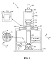
- FIG. 1 schematically depicts a lithographic apparatus 10 according to a particular embodiment of the invention.
- the apparatus 10 includes an illumination system (illuminator) IL for providing a projection beam PB of radiation (e.g. UV radiation or EUV radiation), a first support structure (e.g. a mask table) MT for supporting a patterning device (e.g. a mask) MA and connected to a first positioning device PM for accurately positioning the patterning device with respect to item PL, a substrate table (e.g. a wafer table) WT for holding a substrate (e.g. a resist-coated wafer) W and connected to a second positioning device PW for accurately positioning the substrate with respect to item PL, and a projection system (e.g. a refractive projection lens) PL for imaging a pattern imparted to the projection beam PB by the patterning device MA onto a target portion C (e.g. including one or more dies) of the substrate W.
- an illumination system illumination system
- IL for
- the depicted apparatus may be used in the following example modes:
- the resist 310 may include a bottom anti-reflective coating 320, commonly referred to as a "BARC," that is disposed in between the resist 310 and the at least one feature 300.
- BARC bottom anti-reflective coating 320
- the marker 200 is imaged onto the resist 310 directly over the feature 300 by patterning a beam of radiation with a patterning device that includes an alignment marker. After the marker 200 has been developed, the resist 310 is coated with an opaque coating 330 in such a way that the coating 330 is substantially uniform over the marker 200.
- the operative exposure radiation may have a wavelength of 248 nm
- the wavelength of the beam of light provided by the alignment sensor may be 533 nm and/or 632.8 nm
- the level sensor may use a beam of light with a wavelength of about 900 nm - 1100 nm.
- the ARC should be anti-reflective (i.e. absorbing) at wavelengths that include 248 nm, 533 nm, and 632.8 nm, but be transparent at wavelengths between about 900 nm - 1100 nm.
- the ARC is non-photosensitive.
Landscapes
- Physics & Mathematics (AREA)
- General Physics & Mathematics (AREA)
- Exposure And Positioning Against Photoresist Photosensitive Materials (AREA)
- Exposure Of Semiconductors, Excluding Electron Or Ion Beam Exposure (AREA)
Applications Claiming Priority (2)
| Application Number | Priority Date | Filing Date | Title |
|---|---|---|---|
| US63984704P | 2004-12-29 | 2004-12-29 | |
| US11/135,630 US7355675B2 (en) | 2004-12-29 | 2005-05-24 | Method for measuring information about a substrate, and a substrate for use in a lithographic apparatus |
Publications (2)
| Publication Number | Publication Date |
|---|---|
| EP1677158A2 true EP1677158A2 (de) | 2006-07-05 |
| EP1677158A3 EP1677158A3 (de) | 2006-07-26 |
Family
ID=36090762
Family Applications (1)
| Application Number | Title | Priority Date | Filing Date |
|---|---|---|---|
| EP05258013A Withdrawn EP1677158A3 (de) | 2004-12-29 | 2005-12-22 | Verfahrung zur Messung von Substratinformationen und Substrat für Gebrauch in einem lithografischen Apparat |
Country Status (7)
| Country | Link |
|---|---|
| US (1) | US7355675B2 (de) |
| EP (1) | EP1677158A3 (de) |
| JP (1) | JP4308202B2 (de) |
| KR (1) | KR100724050B1 (de) |
| CN (1) | CN1804726B (de) |
| SG (1) | SG123769A1 (de) |
| TW (1) | TWI323389B (de) |
Cited By (3)
| Publication number | Priority date | Publication date | Assignee | Title |
|---|---|---|---|---|
| WO2009040241A3 (en) * | 2007-09-26 | 2009-06-04 | Ibm | Method and apparatus for measurement and control of photomask to substrate alignment |
| WO2010025793A1 (en) * | 2008-09-08 | 2010-03-11 | Asml Netherlands B.V. | A substrate, a method of measuring a property, an inspection apparatus and a lithographic apparatus |
| CN102967996A (zh) * | 2012-11-02 | 2013-03-13 | 上海华力微电子有限公司 | 一种改善光刻机对准精度的方法 |
Families Citing this family (12)
| Publication number | Priority date | Publication date | Assignee | Title |
|---|---|---|---|---|
| US7432605B2 (en) * | 2006-09-21 | 2008-10-07 | Macronix International Co., Ltd. | Overlay mark, method for forming the same and application thereof |
| US20090208865A1 (en) * | 2008-02-19 | 2009-08-20 | International Business Machines Corporation | Photolithography focus improvement by reduction of autofocus radiation transmission into substrate |
| US8084185B2 (en) * | 2009-01-08 | 2011-12-27 | International Business Machines Corporation | Substrate planarization with imprint materials and processes |
| US8929630B2 (en) * | 2009-03-27 | 2015-01-06 | Life Technologies Corporation | Systems and methods for assessing images |
| US8772376B2 (en) * | 2009-08-18 | 2014-07-08 | International Business Machines Corporation | Near-infrared absorbing film compositions |
| KR102058515B1 (ko) * | 2013-04-18 | 2019-12-24 | 삼성디스플레이 주식회사 | 증착장치, 이를 이용한 유기발광 디스플레이 장치 제조 방법 및 유기발광 디스플레이 장치 |
| CN105080855B (zh) * | 2015-06-03 | 2017-08-25 | 合肥京东方光电科技有限公司 | 基板标记检测装置和基板标记检测方法 |
| US10216096B2 (en) * | 2015-08-14 | 2019-02-26 | Kla-Tencor Corporation | Process-sensitive metrology systems and methods |
| CN106647174B (zh) * | 2015-10-30 | 2018-08-14 | 上海微电子装备(集团)股份有限公司 | 一种调焦调平装置及调焦调平方法 |
| WO2017167637A1 (en) | 2016-03-30 | 2017-10-05 | Asml Netherlands B.V. | Substrate edge detection |
| CN109360333A (zh) * | 2018-10-24 | 2019-02-19 | 深圳市航天电机系统有限公司 | 基于自动售货机的驱动响应结构及工作方法 |
| CN111933618B (zh) * | 2020-08-13 | 2022-01-28 | 武汉新芯集成电路制造有限公司 | 具有对准标识的晶圆组件及其形成方法、晶圆对准方法 |
Citations (2)
| Publication number | Priority date | Publication date | Assignee | Title |
|---|---|---|---|---|
| WO2002023627A1 (en) * | 2000-09-14 | 2002-03-21 | Infineon Technologies North America Corp. | Semiconductor interconnection structure and method of fabrication |
| US20030013281A1 (en) * | 2001-07-11 | 2003-01-16 | Chung Se Jin | Polysilicon crystallizing method, method of fabricating thin film transistor using the same, and method of fabricating liquid crystal display thereof |
Family Cites Families (31)
| Publication number | Priority date | Publication date | Assignee | Title |
|---|---|---|---|---|
| NL186353C (nl) * | 1979-06-12 | 1990-11-01 | Philips Nv | Inrichting voor het afbeelden van een maskerpatroon op een substraat voorzien van een opto-elektronisch detektiestelsel voor het bepalen van een afwijking tussen het beeldvlak van een projektielenzenstelsel en het substraatvlak. |
| JPS59220604A (ja) | 1983-05-30 | 1984-12-12 | Hitachi Ltd | 微小間隙をおいて相対する2物体間の位置検出方法 |
| JPS61248427A (ja) | 1985-04-25 | 1986-11-05 | Nec Corp | 多層配線の形成方法 |
| NL8600639A (nl) * | 1986-03-12 | 1987-10-01 | Asm Lithography Bv | Werkwijze voor het ten opzichte van elkaar uitrichten van een masker en een substraat en inrichting voor het uitvoeren van de werkwijze. |
| JPH0236523A (ja) | 1988-07-27 | 1990-02-06 | Oki Electric Ind Co Ltd | ウエハアライメントマーク及びその形成方法 |
| JPH02229419A (ja) | 1989-03-02 | 1990-09-12 | Fujitsu Ltd | 半導体装置の製造方法 |
| NL9000503A (nl) * | 1990-03-05 | 1991-10-01 | Asm Lithography Bv | Apparaat en werkwijze voor het afbeelden van een maskerpatroon op een substraat. |
| JPH05198471A (ja) | 1992-01-22 | 1993-08-06 | Canon Inc | 基板の位置合わせ方法およびこれに用いる反射マーク付基板 |
| US5601957A (en) * | 1994-06-16 | 1997-02-11 | Nikon Corporation | Micro devices manufacturing method comprising the use of a second pattern overlying an alignment mark to reduce flattening |
| JP3239976B2 (ja) * | 1994-09-30 | 2001-12-17 | 株式会社東芝 | アライメントマーク、半導体装置の製造方法および半導体装置 |
| JP3387075B2 (ja) * | 1994-12-12 | 2003-03-17 | 株式会社ニコン | 走査露光方法、露光装置、及び走査型露光装置 |
| US5982764A (en) * | 1995-05-18 | 1999-11-09 | Aura Communications, Inc. | Time-multiplexed short-range magnetic communications |
| US5960107A (en) * | 1995-12-28 | 1999-09-28 | Vlsi Technology, Inc. | Method for verifying an average topography height function of a photostepper |
| WO1998028665A1 (en) * | 1996-12-24 | 1998-07-02 | Koninklijke Philips Electronics N.V. | Two-dimensionally balanced positioning device with two object holders, and lithographic device provided with such a positioning device |
| JP2947196B2 (ja) * | 1997-01-23 | 1999-09-13 | 日本電気株式会社 | 半導体基板および半導体装置の製造方法 |
| JP3570728B2 (ja) * | 1997-03-07 | 2004-09-29 | アーエスエム リソグラフィ ベスローテン フェンノートシャップ | 離軸整列ユニットを持つリトグラフ投射装置 |
| EP0900412B1 (de) * | 1997-03-10 | 2005-04-06 | ASML Netherlands B.V. | Lithographiegerät mit einer positioniervorrichtung mit zwei objekthaltern |
| US5966613A (en) * | 1997-09-08 | 1999-10-12 | Lsi Corporation | Consistent alignment mark profiles on semiconductor wafers using metal organic chemical vapor deposition titanium nitride protective |
| US5985764A (en) | 1997-12-22 | 1999-11-16 | Taiwan Semiconductor Manufacturing Company, Ltd. | Layer independent alignment system |
| US6452284B1 (en) * | 2000-06-22 | 2002-09-17 | Motorola, Inc. | Semiconductor device substrate and a process for altering a semiconductor device |
| TW497013B (en) * | 2000-09-07 | 2002-08-01 | Asm Lithography Bv | Method for calibrating a lithographic projection apparatus and apparatus capable of applying such a method |
| US20030096496A1 (en) * | 2001-11-20 | 2003-05-22 | I-Hsiung Huang | Method of forming dual damascene structure |
| US6815838B2 (en) * | 2002-02-20 | 2004-11-09 | International Business Machines Corporation | Laser alignment target and method |
| CN1276306C (zh) * | 2002-05-14 | 2006-09-20 | 株式会社东芝 | 加工方法及半导体器件的制造方法 |
| JP4201541B2 (ja) * | 2002-07-19 | 2008-12-24 | 豊田合成株式会社 | 半導体結晶の製造方法及びiii族窒化物系化合物半導体発光素子の製造方法 |
| US20040075179A1 (en) * | 2002-10-22 | 2004-04-22 | United Microelectronics Corp | Structural design of alignment mark |
| US6774452B1 (en) * | 2002-12-17 | 2004-08-10 | Cypress Semiconductor Corporation | Semiconductor structure having alignment marks with shallow trench isolation |
| DE10259322B4 (de) | 2002-12-18 | 2005-12-29 | Infineon Technologies Ag | Verfahren zum Bilden einer Justiermarke in einer lichtundurchlässigen Schicht auf einem Substrat |
| KR100620982B1 (ko) * | 2002-12-19 | 2006-09-13 | 에이에스엠엘 네델란즈 비.브이. | 디바이스 제조방법, 리소그래피장치를 제어하기 위한 컴퓨터 프로그램을 기록한 기록매체 및 리소그래피 장치 |
| KR100495920B1 (ko) * | 2003-06-25 | 2005-06-17 | 주식회사 하이닉스반도체 | 반도체 장치의 웨이퍼 정렬용 정렬 마크 |
| EP1768792A1 (de) * | 2004-06-21 | 2007-04-04 | Ferro Corporation | Verfahren zur herstellung und erfassung von unsichtbaren markierungen und gemäss den verfahren markierte artikel |
-
2005
- 2005-05-24 US US11/135,630 patent/US7355675B2/en not_active Expired - Fee Related
- 2005-12-22 EP EP05258013A patent/EP1677158A3/de not_active Withdrawn
- 2005-12-23 TW TW094146398A patent/TWI323389B/zh not_active IP Right Cessation
- 2005-12-23 SG SG200508373A patent/SG123769A1/en unknown
- 2005-12-27 CN CN2005101191488A patent/CN1804726B/zh not_active Expired - Fee Related
- 2005-12-27 KR KR1020050130907A patent/KR100724050B1/ko not_active Expired - Fee Related
- 2005-12-28 JP JP2005376941A patent/JP4308202B2/ja not_active Expired - Fee Related
Patent Citations (2)
| Publication number | Priority date | Publication date | Assignee | Title |
|---|---|---|---|---|
| WO2002023627A1 (en) * | 2000-09-14 | 2002-03-21 | Infineon Technologies North America Corp. | Semiconductor interconnection structure and method of fabrication |
| US20030013281A1 (en) * | 2001-07-11 | 2003-01-16 | Chung Se Jin | Polysilicon crystallizing method, method of fabricating thin film transistor using the same, and method of fabricating liquid crystal display thereof |
Cited By (9)
| Publication number | Priority date | Publication date | Assignee | Title |
|---|---|---|---|---|
| WO2009040241A3 (en) * | 2007-09-26 | 2009-06-04 | Ibm | Method and apparatus for measurement and control of photomask to substrate alignment |
| US7875987B2 (en) | 2007-09-26 | 2011-01-25 | International Business Machines Corporation | Method and apparatus for measurement and control of photomask to substrate alignment |
| US7989968B2 (en) | 2007-09-26 | 2011-08-02 | International Business Machines Corporation | Method and apparatus for measurement and control of photomask to substrate alignment |
| US8003412B2 (en) | 2007-09-26 | 2011-08-23 | International Business Machines Corporation | Method and apparatus for measurement and control of photomask to substrate alignment |
| US8138089B2 (en) | 2007-09-26 | 2012-03-20 | International Business Machines Corporation | Method and apparatus for measurement and control of photomask to substrate alignment |
| WO2010025793A1 (en) * | 2008-09-08 | 2010-03-11 | Asml Netherlands B.V. | A substrate, a method of measuring a property, an inspection apparatus and a lithographic apparatus |
| US9229338B2 (en) | 2008-09-08 | 2016-01-05 | Asml Netherlands B.V. | Substrate, a method of measuring a property, an inspection apparatus and a lithographic apparatus |
| US9255892B2 (en) | 2008-09-08 | 2016-02-09 | Asml Netherlands B.V. | Substrate, a method of measuring a property, an inspection apparatus and a lithographic apparatus |
| CN102967996A (zh) * | 2012-11-02 | 2013-03-13 | 上海华力微电子有限公司 | 一种改善光刻机对准精度的方法 |
Also Published As
| Publication number | Publication date |
|---|---|
| CN1804726A (zh) | 2006-07-19 |
| US20060138410A1 (en) | 2006-06-29 |
| EP1677158A3 (de) | 2006-07-26 |
| JP4308202B2 (ja) | 2009-08-05 |
| KR100724050B1 (ko) | 2007-06-04 |
| TWI323389B (en) | 2010-04-11 |
| KR20060093010A (ko) | 2006-08-23 |
| TW200632583A (en) | 2006-09-16 |
| CN1804726B (zh) | 2011-04-13 |
| JP2006191080A (ja) | 2006-07-20 |
| SG123769A1 (en) | 2006-07-26 |
| US7355675B2 (en) | 2008-04-08 |
Similar Documents
| Publication | Publication Date | Title |
|---|---|---|
| JP4541374B2 (ja) | 基板計測のための縮小されたスクライブレーンの使用を有するリソグラフィ装置およびデバイス製造方法 | |
| US8797554B2 (en) | Determining a structural parameter and correcting an asymmetry property | |
| US20200124543A1 (en) | Diffraction Based Overlay Metrology Tool and Method of Diffraction Based Overlay Metrology | |
| JP4234567B2 (ja) | リソグラフィ装置及びデバイス製造方法 | |
| TWI253682B (en) | Substrate provided with an alignment mark, method of designing a mask, computer program, mask for exposing said mark, device manufacturing method, and device manufactured thereby | |
| US8120001B2 (en) | Inspection method and apparatus, lithographic apparatus, lithographic processing cell and device manufacturing method | |
| US20090244538A1 (en) | Lithographic Apparatus and Device Manufacturing Method Using Overlay Measurement | |
| JP2010109377A (ja) | リソグラフィ装置及び測定方法 | |
| CN101592872A (zh) | 确定衬底中的缺陷的方法和光刻工艺中曝光衬底的设备 | |
| US7355675B2 (en) | Method for measuring information about a substrate, and a substrate for use in a lithographic apparatus | |
| CN1641484A (zh) | 测量方法、用于提供对准标记的方法和器件制造方法 | |
| WO2019048216A1 (en) | PATTERNS OF BEAT FOR ALIGNMENT ON SMALL TARGETS OF METROLOGY | |
| US7781237B2 (en) | Alignment marker and lithographic apparatus and device manufacturing method using the same | |
| US7835017B2 (en) | Lithographic apparatus, method of exposing a substrate, method of measurement, device manufacturing method, and device manufactured thereby | |
| US6862076B2 (en) | Method of determining stray radiation lithographic projection apparatus | |
| KR100734589B1 (ko) | 기판 테이블, 기판의 위치를 측정하는 방법, 및 리소그래피장치 | |
| US7283236B2 (en) | Alignment system and lithographic apparatus equipped with such an alignment system | |
| KR20090101123A (ko) | 리소그래피 장치에서의 개략적인 웨이퍼 정렬을 위한 방법 | |
| US6987555B2 (en) | Lithographic apparatus, device manufacturing method, and device manufactured thereby | |
| US7821650B2 (en) | Lithographic apparatus and device manufacturing method with reduced scribe lane usage for substrate measurement | |
| US20060141375A1 (en) | Exposure apparatus, a tilting device method for performing a tilted focus test, and a device manufactured accordingly | |
| EP1400860B1 (de) | Lithographische Markierungsstruktur, lithographischer Projektionsapparat mit einer solchen Markierungsstruktur und Verfahren zur Ausrichtung eines Substrates unter Verwendung einer solchen Markierungsstruktur | |
| US7136149B2 (en) | Lithographic apparatus with autofocus system |
Legal Events
| Date | Code | Title | Description |
|---|---|---|---|
| PUAI | Public reference made under article 153(3) epc to a published international application that has entered the european phase |
Free format text: ORIGINAL CODE: 0009012 |
|
| PUAL | Search report despatched |
Free format text: ORIGINAL CODE: 0009013 |
|
| AK | Designated contracting states |
Kind code of ref document: A2 Designated state(s): AT BE BG CH CY CZ DE DK EE ES FI FR GB GR HU IE IS IT LI LT LU LV MC NL PL PT RO SE SI SK TR |
|
| AX | Request for extension of the european patent |
Extension state: AL BA HR MK YU |
|
| AK | Designated contracting states |
Kind code of ref document: A3 Designated state(s): AT BE BG CH CY CZ DE DK EE ES FI FR GB GR HU IE IS IT LI LT LU LV MC NL PL PT RO SE SI SK TR |
|
| AX | Request for extension of the european patent |
Extension state: AL BA HR MK YU |
|
| 17P | Request for examination filed |
Effective date: 20070125 |
|
| AKX | Designation fees paid |
Designated state(s): DE FR GB IT NL |
|
| 17Q | First examination report despatched |
Effective date: 20070523 |
|
| STAA | Information on the status of an ep patent application or granted ep patent |
Free format text: STATUS: THE APPLICATION IS DEEMED TO BE WITHDRAWN |
|
| 18D | Application deemed to be withdrawn |
Effective date: 20140701 |