EP1699089A1 - Méthode et moule pour la fabrication d'un module semiconducteur optique - Google Patents
Méthode et moule pour la fabrication d'un module semiconducteur optique Download PDFInfo
- Publication number
- EP1699089A1 EP1699089A1 EP06003875A EP06003875A EP1699089A1 EP 1699089 A1 EP1699089 A1 EP 1699089A1 EP 06003875 A EP06003875 A EP 06003875A EP 06003875 A EP06003875 A EP 06003875A EP 1699089 A1 EP1699089 A1 EP 1699089A1
- Authority
- EP
- European Patent Office
- Prior art keywords
- optically active
- semiconductor
- base body
- casting mold
- leadframe
- Prior art date
- Legal status (The legal status is an assumption and is not a legal conclusion. Google has not performed a legal analysis and makes no representation as to the accuracy of the status listed.)
- Granted
Links
Images


Classifications
-
- H—ELECTRICITY
- H10—SEMICONDUCTOR DEVICES; ELECTRIC SOLID-STATE DEVICES NOT OTHERWISE PROVIDED FOR
- H10F—INORGANIC SEMICONDUCTOR DEVICES SENSITIVE TO INFRARED RADIATION, LIGHT, ELECTROMAGNETIC RADIATION OF SHORTER WAVELENGTH OR CORPUSCULAR RADIATION
- H10F77/00—Constructional details of devices covered by this subclass
- H10F77/50—Encapsulations or containers
-
- B—PERFORMING OPERATIONS; TRANSPORTING
- B29—WORKING OF PLASTICS; WORKING OF SUBSTANCES IN A PLASTIC STATE IN GENERAL
- B29C—SHAPING OR JOINING OF PLASTICS; SHAPING OF MATERIAL IN A PLASTIC STATE, NOT OTHERWISE PROVIDED FOR; AFTER-TREATMENT OF THE SHAPED PRODUCTS, e.g. REPAIRING
- B29C33/00—Moulds or cores; Details thereof or accessories therefor
- B29C33/0038—Moulds or cores; Details thereof or accessories therefor with sealing means or the like
- B29C33/0044—Moulds or cores; Details thereof or accessories therefor with sealing means or the like for sealing off parts of inserts projecting into the mould cavity
-
- B—PERFORMING OPERATIONS; TRANSPORTING
- B29—WORKING OF PLASTICS; WORKING OF SUBSTANCES IN A PLASTIC STATE IN GENERAL
- B29C—SHAPING OR JOINING OF PLASTICS; SHAPING OF MATERIAL IN A PLASTIC STATE, NOT OTHERWISE PROVIDED FOR; AFTER-TREATMENT OF THE SHAPED PRODUCTS, e.g. REPAIRING
- B29C39/00—Shaping by casting, i.e. introducing the moulding material into a mould or between confining surfaces without significant moulding pressure; Apparatus therefor
- B29C39/02—Shaping by casting, i.e. introducing the moulding material into a mould or between confining surfaces without significant moulding pressure; Apparatus therefor for making articles of definite length, i.e. discrete articles
- B29C39/10—Shaping by casting, i.e. introducing the moulding material into a mould or between confining surfaces without significant moulding pressure; Apparatus therefor for making articles of definite length, i.e. discrete articles incorporating preformed parts or layers, e.g. casting around inserts or for coating articles
-
- B—PERFORMING OPERATIONS; TRANSPORTING
- B29—WORKING OF PLASTICS; WORKING OF SUBSTANCES IN A PLASTIC STATE IN GENERAL
- B29C—SHAPING OR JOINING OF PLASTICS; SHAPING OF MATERIAL IN A PLASTIC STATE, NOT OTHERWISE PROVIDED FOR; AFTER-TREATMENT OF THE SHAPED PRODUCTS, e.g. REPAIRING
- B29C39/00—Shaping by casting, i.e. introducing the moulding material into a mould or between confining surfaces without significant moulding pressure; Apparatus therefor
- B29C39/22—Component parts, details or accessories; Auxiliary operations
- B29C39/26—Moulds or cores
-
- H—ELECTRICITY
- H10—SEMICONDUCTOR DEVICES; ELECTRIC SOLID-STATE DEVICES NOT OTHERWISE PROVIDED FOR
- H10H—INORGANIC LIGHT-EMITTING SEMICONDUCTOR DEVICES HAVING POTENTIAL BARRIERS
- H10H20/00—Individual inorganic light-emitting semiconductor devices having potential barriers, e.g. light-emitting diodes [LED]
- H10H20/80—Constructional details
- H10H20/85—Packages
- H10H20/852—Encapsulations
- H10H20/853—Encapsulations characterised by their shape
-
- H—ELECTRICITY
- H10—SEMICONDUCTOR DEVICES; ELECTRIC SOLID-STATE DEVICES NOT OTHERWISE PROVIDED FOR
- H10W—GENERIC PACKAGES, INTERCONNECTIONS, CONNECTORS OR OTHER CONSTRUCTIONAL DETAILS OF DEVICES COVERED BY CLASS H10
- H10W72/00—Interconnections or connectors in packages
- H10W72/50—Bond wires
- H10W72/531—Shapes of wire connectors
- H10W72/536—Shapes of wire connectors the connected ends being ball-shaped
-
- H—ELECTRICITY
- H10—SEMICONDUCTOR DEVICES; ELECTRIC SOLID-STATE DEVICES NOT OTHERWISE PROVIDED FOR
- H10W—GENERIC PACKAGES, INTERCONNECTIONS, CONNECTORS OR OTHER CONSTRUCTIONAL DETAILS OF DEVICES COVERED BY CLASS H10
- H10W72/00—Interconnections or connectors in packages
- H10W72/50—Bond wires
- H10W72/531—Shapes of wire connectors
- H10W72/5363—Shapes of wire connectors the connected ends being wedge-shaped
-
- H—ELECTRICITY
- H10—SEMICONDUCTOR DEVICES; ELECTRIC SOLID-STATE DEVICES NOT OTHERWISE PROVIDED FOR
- H10W—GENERIC PACKAGES, INTERCONNECTIONS, CONNECTORS OR OTHER CONSTRUCTIONAL DETAILS OF DEVICES COVERED BY CLASS H10
- H10W72/00—Interconnections or connectors in packages
- H10W72/50—Bond wires
- H10W72/541—Dispositions of bond wires
- H10W72/5449—Dispositions of bond wires not being orthogonal to a side surface of the chip, e.g. fan-out arrangements
-
- H—ELECTRICITY
- H10—SEMICONDUCTOR DEVICES; ELECTRIC SOLID-STATE DEVICES NOT OTHERWISE PROVIDED FOR
- H10W—GENERIC PACKAGES, INTERCONNECTIONS, CONNECTORS OR OTHER CONSTRUCTIONAL DETAILS OF DEVICES COVERED BY CLASS H10
- H10W74/00—Encapsulations, e.g. protective coatings
- H10W74/01—Manufacture or treatment
- H10W74/016—Manufacture or treatment using moulds
-
- H—ELECTRICITY
- H10—SEMICONDUCTOR DEVICES; ELECTRIC SOLID-STATE DEVICES NOT OTHERWISE PROVIDED FOR
- H10W—GENERIC PACKAGES, INTERCONNECTIONS, CONNECTORS OR OTHER CONSTRUCTIONAL DETAILS OF DEVICES COVERED BY CLASS H10
- H10W90/00—Package configurations
- H10W90/701—Package configurations characterised by the relative positions of pads or connectors relative to package parts
- H10W90/751—Package configurations characterised by the relative positions of pads or connectors relative to package parts of bond wires
- H10W90/756—Package configurations characterised by the relative positions of pads or connectors relative to package parts of bond wires between a chip and a stacked lead frame, conducting package substrate or heat sink
Definitions
- the invention relates to a method and a mold for producing an optical semiconductor module, wherein a semiconductor base body, which has at least one optically active element on its surface, is introduced into a leadframe, conductive connections between the semiconductor base body and the leadframe are produced thereon and leadframe and Semiconductor body are cast in a mold.
- Such manufacturing methods are known from the prior art in which an optical IC (PDIC) is encapsulated with a transparent encapsulant or arranged on an organic substrate and then covered with a potting compound.
- the potting compound must be transparent in order to allow radiations in the optical range to pass from or to the optically active element. In this case, the potting compound must be matched to the wavelength range in which the optical element transmits or receives. In addition, the potting compound must be temperature-stable and long-term stable and moisture-resistant.
- the present invention is based on the object to avoid the disadvantages of the prior art and to provide a method for producing an optical semiconductor module of the type mentioned, in which an inexpensive potting compound can be used and the desirable optical properties of the semiconductor module can be achieved. According to the invention, this object is achieved by a method having the features of patent claim 1 and by a casting mold having the features of claim 9.
- the semiconductor module according to the invention is defined in claim 15.
- a semiconductor module can be produced in a particularly simple and cost-effective manner which, on the one hand, is encapsulated and protected from environmental influences such as shocks or moisture, but on the other hand in the region in which light is to be received or emitted, the corresponding potting compound is excluded.
- a more cost-effective potting compound for example, a non-optically transparent epoxy resin can be used, resulting in high cost savings.
- the casting compounds used can thus be selected according to other criteria than after the optical transmission and thus the module can be additionally optimized to other needs.
- each optically active element on the semiconductor base body may be assigned its own cover body or a plurality of the optically active elements may be covered by a cover body together.
- the mold After casting and extensive solidification of the potting compound, the mold can be opened in each case and the cover can be pulled out with the top of the semiconductor body facing part of the mold.
- the end faces of the cover elements are pressed against the semiconductor base body during the casting process in such a way that the low-viscosity casting compound can not penetrate between the end face of the cover body and the corresponding region of the semiconductor base body.
- the semiconductor base body is resiliently held in a leadframe, so that with a corresponding length of the cover body they can push back against the spring force, the semiconductor body a little way, so as to produce the corresponding pressure force.
- the semiconductor base body is covered on its top side with a polyimide layer before casting, whereby the areas of the optically active elements are left free.
- the polyimide layer helps to reduce the thermal stress on the semiconductor body in the resulting potting and makes the semiconductor module temperature stable and thus usable at higher temperatures. This is particularly important if the semiconductor module is further processed by means of lead-free soldering or connected to other circuit units, since in lead-free soldering the corresponding solders require an increased soldering temperature by about 20 ° C with otherwise identical joining conditions.
- the casting mold according to the invention essentially corresponds in terms of its outer structure to a known casting mold for resilient leadframes of the QFN type (Quad flat non-leaded package), wherein additionally the covering bodies are arranged and fastened on an inner wall.
- Such molds are typically made of steel and the cover bodies may be integrally connected to the mold.
- the cover bodies may typically be formed as cylindrical pins, but they may also be slightly conical or taper towards the Semiconductor base toward stepped, conical or convex or concave reducing cross-section, which facilitates the final molding after the casting process. In any case, they have an end face which can be pressed against the semiconductor base body.
- the cover body In cross-section, the cover body may be round or polygonal, preferably quadrangular. Even with a quadrangular shape, the cover body can taper towards the semiconductor base body in order to facilitate removal from the mold.
- the end face of the covering body In order to facilitate the sealing of the optically active regions of the semiconductor base body to be protected by the end face of the covering body, it may be provided that they have a raised edge on their end face, which rotates flatly and forms a sealing edge with respect to the semiconductor base body. If the actual end face is retracted behind this edge, it is also effectively prevented that the casting material is drawn by capillary action into the intermediate space between the semiconductor base body and the covering body.
- the resulting semiconductor module is characterized by its simple design and low price, which is due to the simple encapsulation, leaving the optically active areas. Through the corresponding recesses in the casting material, the emission and reception of optical signals is possible.
- the semiconductor module according to the invention is extremely temperature-stable.
- FIG. 1 shows a cross-section of a potted semiconductor module, in which a semiconductor base body 1 is mounted on a substrate 2 and this unit is resiliently mounted on a leadframe, the parts of which are designated 3, 4.
- the potting material which is typically formed by an epoxy resin, is denoted by 5.
- the parts 3, 4 of the leadframe each form individual contacts, which are connected via bonding wires 6, 7 with respective bonding surfaces 8, 9 of the semiconductor base body.
- the individual contacts 3, 4 are formed after the casting and curing of the semiconductor module by sawing from a contiguous metal body. This consists of prior to the production of the semiconductor module a coherent frame of uniform material, such as copper, in which are formed by etching or pre-punching points at which the individual contacts can be easily separated later. As a result, this frame is easy to process and can still be disassembled later after casting in many against each other electrically isolated items.
- FIG. 1 shows that the semiconductor base body 1 is only partially covered by the casting material 5. There remains a free space 10 in which optically active elements can be arranged, which can then emit or receive radiation without being hindered by the casting material 5.
- the coating of the semiconductor base body 1 with a thin polyimide layer wherein the area 10 and the areas 8, 9, where later bonded, are excluded.
- the substrate 2 may be formed for example by a ceramic, an organic material or a metal.
- the conductivity does not matter because the electrically active zone of the semiconductor body is located exclusively on its upper side.
- FIG. 2 shows the semiconductor module from FIG. 1 in a view from below, where the isolated contacts 3, 4 are open and can be seen.
- FIG. 3 shows an external view of the semiconductor module from the front side.
- FIG. 4 shows a three-dimensional view of the semiconductor module, wherein the potting material is shown transparent such that the bonding wires 6, 7 as well as the parts of the leadframe are visible.
- the bonding wires lead to the semiconductor base body 1, where they end on bonding surfaces 8, 9. It is a recess 10 shown in the casting material, which leaves the optically active elements of the semiconductor body 1 for the emission and reception of optical radiation.
- FIG. 5 shows the semiconductor module from FIG. 4 in a cut three-dimensional form.
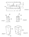
- FIG. 6 very schematically shows a casting mold 11, 12 for a semiconductor module according to the invention.
- Such casting molds are typically combined in many ways in order to create as many semiconductor modules as possible by means of a potting process, but only a single mold is shown in the figure, which consists of a lower part 11 and an upper part 12.
- the upper part 11 carries on its inside 13 two cover body 14, 15, which are formed as cylindrical rods with end faces 16, 17.
- the mold is first closed after inserting the leadframe and the semiconductor base body on the substrate, which are already connected to each other by bonding.
- the cover body 14, 15 with their end faces 16, 17 encounter the semiconductor base body and cover on this the optically active areas.
- After closing the mold is then filled through an inlet opening at low temperatures thin epoxy resin as potting material until the interior of the mold 11, 12 is filled.
- the top of the mold 12 is removed and the cover body 14, 15 are pulled out of the hardened epoxy resin. There remain openings in the casting resin, which extend to the semiconductor body and there leave the optically active areas.
- FIG. 7 shows in a longitudinal section a cylindrical covering body 18, which has an end face 19 with a trough-like depression, the edge 20 of which runs flat and forms a cutting edge, which forms a casting-tight covering in relation to the semiconductor base body during casting.
- FIG. 8 shows a further covering body 21, which is likewise cylindrical and which has on its end face 22 a circumferential web 23 which forms a sealing surface with respect to the semiconductor base body.
- FIG. 9 shows a conically tapered truncated cone 24, which has a planar end face 25 for placement on the semiconductor base body, while FIG. 10 shows a truncated cone 26 with a planar end face 27 which is quadrangular in cross section.
Landscapes
- Engineering & Computer Science (AREA)
- Mechanical Engineering (AREA)
- Led Device Packages (AREA)
- Structures Or Materials For Encapsulating Or Coating Semiconductor Devices Or Solid State Devices (AREA)
- Light Receiving Elements (AREA)
Applications Claiming Priority (1)
| Application Number | Priority Date | Filing Date | Title |
|---|---|---|---|
| DE102005010311A DE102005010311A1 (de) | 2005-03-03 | 2005-03-03 | Verfahren und Gießform zur Herstellung eines optischen Halbleitermoduls |
Publications (2)
| Publication Number | Publication Date |
|---|---|
| EP1699089A1 true EP1699089A1 (fr) | 2006-09-06 |
| EP1699089B1 EP1699089B1 (fr) | 2008-04-23 |
Family
ID=36570921
Family Applications (1)
| Application Number | Title | Priority Date | Filing Date |
|---|---|---|---|
| EP06003875A Expired - Lifetime EP1699089B1 (fr) | 2005-03-03 | 2006-02-25 | Méthode et moule pour la fabrication d'un module semiconducteur optique |
Country Status (4)
| Country | Link |
|---|---|
| US (1) | US7740465B2 (fr) |
| EP (1) | EP1699089B1 (fr) |
| CN (2) | CN1828855A (fr) |
| DE (2) | DE102005010311A1 (fr) |
Families Citing this family (10)
| Publication number | Priority date | Publication date | Assignee | Title |
|---|---|---|---|---|
| EP2192825A1 (fr) * | 2008-11-26 | 2010-06-02 | Osram Gesellschaft mit Beschränkter Haftung | Dispositif de moulage par injection pour encapsuler les circuits électroniques avec des sources lumineuses, et processus d'encapsulation associé |
| WO2011128499A1 (fr) * | 2010-04-14 | 2011-10-20 | Nokia Corporation | Procédé et appareil pour fournir un paiement automatisé |
| CN102956600A (zh) * | 2012-11-20 | 2013-03-06 | 无锡市威海达机械制造有限公司 | 一种引线框架结构 |
| CN102969297A (zh) * | 2012-11-20 | 2013-03-13 | 无锡市威海达机械制造有限公司 | 一种浇铸槽型引线框架结构 |
| JP5788612B2 (ja) * | 2012-11-30 | 2015-10-07 | 楽天株式会社 | 電子マネーシステム、電子バリュー移転方法、携帯端末、携帯端末の制御方法、プログラム及びプログラムが記録された記録媒体 |
| US9269597B2 (en) * | 2013-01-23 | 2016-02-23 | Microchip Technology Incorporated | Open cavity plastic package |
| DE102013206225A1 (de) | 2013-04-09 | 2014-10-09 | Osram Opto Semiconductors Gmbh | Optoelektronisches Bauelement und Verfahren zu seiner Herstellung |
| DE102013207308B4 (de) | 2013-04-23 | 2023-01-12 | OSRAM Opto Semiconductors Gesellschaft mit beschränkter Haftung | Verfahren zum Herstellen einer optoelektronischen Baugruppe und optoelektronische Baugruppe |
| JP6526323B2 (ja) * | 2016-04-04 | 2019-06-05 | 三菱電機株式会社 | パワーモジュール、パワー半導体装置及びパワーモジュール製造方法 |
| CN115476457B (zh) * | 2022-10-27 | 2026-02-03 | 深圳市联影高端医疗装备创新研究院 | 一种模具和接线组件浇筑成型的方法 |
Citations (3)
| Publication number | Priority date | Publication date | Assignee | Title |
|---|---|---|---|---|
| EP0789334A2 (fr) * | 1996-01-26 | 1997-08-13 | Harris Corporation | Dispositif de circuit intégré à ouverture exposant une puce de circuit intégré et procédés associés |
| US5811799A (en) * | 1997-07-31 | 1998-09-22 | Wu; Liang-Chung | Image sensor package having a wall with a sealed cover |
| EP1220309A1 (fr) * | 2000-12-28 | 2002-07-03 | STMicroelectronics S.r.l. | Procédé de fabrication d'un empaquetage pour dispositif électronique |
Family Cites Families (12)
| Publication number | Priority date | Publication date | Assignee | Title |
|---|---|---|---|---|
| JPS60239043A (ja) * | 1984-05-14 | 1985-11-27 | Oki Electric Ind Co Ltd | 半導体装置用パツケ−ジの製造方法 |
| ATE37619T1 (de) * | 1984-07-16 | 1988-10-15 | Siemens Ag | Integrierte konstantstromquelle. |
| JPH0724287B2 (ja) * | 1987-02-12 | 1995-03-15 | 三菱電機株式会社 | 光透過用窓を有する半導体装置とその製造方法 |
| US5438216A (en) * | 1992-08-31 | 1995-08-01 | Motorola, Inc. | Light erasable multichip module |
| KR970005706B1 (ko) * | 1994-01-24 | 1997-04-19 | 금성일렉트론 주식회사 | 고체촬상소자 및 그 제조방법 |
| NL1003315C2 (nl) * | 1996-06-11 | 1997-12-17 | Europ Semiconductor Assembly E | Werkwijze voor het inkapselen van een geïntegreerde halfgeleiderschake- ling. |
| DE19829197C2 (de) * | 1998-06-30 | 2002-06-20 | Siemens Ag | Strahlungsaussendendes und/oder -empfangendes Bauelement |
| US6441503B1 (en) * | 2001-01-03 | 2002-08-27 | Amkor Technology, Inc. | Bond wire pressure sensor die package |
| NL1019042C2 (nl) * | 2001-09-26 | 2003-03-27 | Europ Semiconductor Assembly E | Werkwijze voor het inkapselen van een chip en/of ander voorwerp. |
| JP3908971B2 (ja) | 2001-10-11 | 2007-04-25 | 浜松ホトニクス株式会社 | 発光素子駆動回路 |
| JP3988469B2 (ja) * | 2002-01-25 | 2007-10-10 | ソニー株式会社 | 半導体レーザ駆動回路 |
| SG143932A1 (en) * | 2003-05-30 | 2008-07-29 | Micron Technology Inc | Packaged microelectronic devices and methods of packaging microelectronic devices |
-
2005
- 2005-03-03 DE DE102005010311A patent/DE102005010311A1/de not_active Withdrawn
-
2006
- 2006-02-25 DE DE502006000667T patent/DE502006000667D1/de not_active Expired - Lifetime
- 2006-02-25 EP EP06003875A patent/EP1699089B1/fr not_active Expired - Lifetime
- 2006-03-03 US US11/366,482 patent/US7740465B2/en not_active Expired - Fee Related
- 2006-03-03 CN CN200610059419.XA patent/CN1828855A/zh active Pending
- 2006-03-03 CN CN201410280133.9A patent/CN104149244A/zh active Pending
Patent Citations (3)
| Publication number | Priority date | Publication date | Assignee | Title |
|---|---|---|---|---|
| EP0789334A2 (fr) * | 1996-01-26 | 1997-08-13 | Harris Corporation | Dispositif de circuit intégré à ouverture exposant une puce de circuit intégré et procédés associés |
| US5811799A (en) * | 1997-07-31 | 1998-09-22 | Wu; Liang-Chung | Image sensor package having a wall with a sealed cover |
| EP1220309A1 (fr) * | 2000-12-28 | 2002-07-03 | STMicroelectronics S.r.l. | Procédé de fabrication d'un empaquetage pour dispositif électronique |
Also Published As
| Publication number | Publication date |
|---|---|
| US20060196412A1 (en) | 2006-09-07 |
| EP1699089B1 (fr) | 2008-04-23 |
| DE502006000667D1 (de) | 2008-06-05 |
| CN104149244A (zh) | 2014-11-19 |
| DE102005010311A1 (de) | 2006-09-14 |
| US7740465B2 (en) | 2010-06-22 |
| CN1828855A (zh) | 2006-09-06 |
Similar Documents
| Publication | Publication Date | Title |
|---|---|---|
| EP2532034B1 (fr) | Composant optoélectronique et procédé de fabrication d'un composant optoélectronique | |
| EP0931343B1 (fr) | Module puce en particulier pour implantation dans un corps de carte a puce | |
| DE102008060615B4 (de) | Licht aussendende Diode | |
| EP2606510B1 (fr) | Procédé de fabrication d'au moins un composant semi-conducteur optoélectronique | |
| DE10297164T5 (de) | Flächig befestigbare Optokoppler-Packung | |
| WO2012000943A1 (fr) | Procédé de fabrication d'un composant semiconducteur pouvant être monté en surface | |
| EP2396832A1 (fr) | Dispositif semi-conducteur optoélectronique encapsulé à couche d'arrêt brasée, et procédé correspondant | |
| DE112014001884B4 (de) | Optoelektronisches Bauelement, Trägerverbund zur Herstellung optoelektronischer Bauelemente und Verfahren zur Herstellung optoelektronischer Bauelemente | |
| EP1699089B1 (fr) | Méthode et moule pour la fabrication d'un module semiconducteur optique | |
| DE102015115824A1 (de) | Optoelektronisches Bauelement | |
| DE4230030A1 (de) | Halbleitergehaeuse und verfahren zu dessen zusammenbau | |
| DE102015101561A1 (de) | Halbleiterpaket und verfahren zur herstellung eines halbleiterpakets | |
| DE69417329T2 (de) | In Harz versiegelte Halbleiteranordnung | |
| WO2005064696A1 (fr) | Composant semi-conducteur emetteur de rayonnement et/ou recepteur de rayonnement, et son procede de fabrication | |
| EP2351462A1 (fr) | Procédé de fabrication d'un élément de conversion de luminescence, élément de conversion de luminescence, et composant optoélectronique | |
| WO2004107511A2 (fr) | Procede de production d'un composant a diodes laser, boitier pour composant a diodes laser, et composant a diodes laser y relatif | |
| DE102014117353A1 (de) | Auswerferstift und Verfahren zum Herstellen desselben | |
| DE112014002023B4 (de) | Optoelektronisches Bauelement und Verfahren zu seiner Herstellung | |
| DE102012207593A1 (de) | Verfahren zum herstellen von bauteilen, bauteile und formwerkzeug | |
| DE4319786A1 (de) | In Kunststoff gegossene CCD-Einheit und Verfahren zu deren Herstellung | |
| EP1318549A2 (fr) | Procédé de fabrication d'un composant semiconducteur optoélectronique | |
| DE102015101070A1 (de) | Optoelektronisches Halbleiterbauteil, optoelektronische Anordnung und Verfahren zur Herstellung eines optoelektronischen Halbleiterbauteils | |
| DE102017219325A1 (de) | Spritzwerkzeug und Verfahren zur Abdichtung von Einlegeteilen | |
| DE102013220960A1 (de) | Optoelektronisches Bauelement und Verfahren zu seiner Herstellung | |
| DE2028821A1 (de) | Gehäuse fur eine Halbleitervor richtung |
Legal Events
| Date | Code | Title | Description |
|---|---|---|---|
| PUAI | Public reference made under article 153(3) epc to a published international application that has entered the european phase |
Free format text: ORIGINAL CODE: 0009012 |
|
| 17P | Request for examination filed |
Effective date: 20060225 |
|
| AK | Designated contracting states |
Kind code of ref document: A1 Designated state(s): AT BE BG CH CY CZ DE DK EE ES FI FR GB GR HU IE IS IT LI LT LU LV MC NL PL PT RO SE SI SK TR |
|
| AX | Request for extension of the european patent |
Extension state: AL BA HR MK YU |
|
| 17Q | First examination report despatched |
Effective date: 20061016 |
|
| AKX | Designation fees paid |
Designated state(s): DE FR |
|
| GRAP | Despatch of communication of intention to grant a patent |
Free format text: ORIGINAL CODE: EPIDOSNIGR1 |
|
| GRAS | Grant fee paid |
Free format text: ORIGINAL CODE: EPIDOSNIGR3 |
|
| GRAA | (expected) grant |
Free format text: ORIGINAL CODE: 0009210 |
|
| AK | Designated contracting states |
Kind code of ref document: B1 Designated state(s): DE FR |
|
| REF | Corresponds to: |
Ref document number: 502006000667 Country of ref document: DE Date of ref document: 20080605 Kind code of ref document: P |
|
| ET | Fr: translation filed | ||
| PLBE | No opposition filed within time limit |
Free format text: ORIGINAL CODE: 0009261 |
|
| STAA | Information on the status of an ep patent application or granted ep patent |
Free format text: STATUS: NO OPPOSITION FILED WITHIN TIME LIMIT |
|
| 26N | No opposition filed |
Effective date: 20090126 |
|
| PGFP | Annual fee paid to national office [announced via postgrant information from national office to epo] |
Ref country code: FR Payment date: 20090220 Year of fee payment: 4 |
|
| REG | Reference to a national code |
Ref country code: FR Ref legal event code: ST Effective date: 20101029 |
|
| PG25 | Lapsed in a contracting state [announced via postgrant information from national office to epo] |
Ref country code: FR Free format text: LAPSE BECAUSE OF NON-PAYMENT OF DUE FEES Effective date: 20100301 |
|
| REG | Reference to a national code |
Ref country code: DE Ref legal event code: R082 Ref document number: 502006000667 Country of ref document: DE Representative=s name: GRUENECKER, KINKELDEY, STOCKMAIR & SCHWANHAEUS, DE Effective date: 20130529 Ref country code: DE Ref legal event code: R081 Ref document number: 502006000667 Country of ref document: DE Owner name: ATMEL CORP., US Free format text: FORMER OWNER: ATMEL AUTOMOTIVE GMBH, 74072 HEILBRONN, DE Effective date: 20130529 Ref country code: DE Ref legal event code: R081 Ref document number: 502006000667 Country of ref document: DE Owner name: ATMEL CORP., SAN JOSE, US Free format text: FORMER OWNER: ATMEL AUTOMOTIVE GMBH, 74072 HEILBRONN, DE Effective date: 20130529 Ref country code: DE Ref legal event code: R082 Ref document number: 502006000667 Country of ref document: DE Representative=s name: GRUENECKER PATENT- UND RECHTSANWAELTE PARTG MB, DE Effective date: 20130529 |
|
| PGFP | Annual fee paid to national office [announced via postgrant information from national office to epo] |
Ref country code: DE Payment date: 20160216 Year of fee payment: 11 |
|
| REG | Reference to a national code |
Ref country code: DE Ref legal event code: R119 Ref document number: 502006000667 Country of ref document: DE |
|
| PG25 | Lapsed in a contracting state [announced via postgrant information from national office to epo] |
Ref country code: DE Free format text: LAPSE BECAUSE OF NON-PAYMENT OF DUE FEES Effective date: 20170901 |