EP1699135A2 - Ausgang Schaltung mit kleiner Differentielle Amplitude und Schnittstelle für Serielle Übertragung - Google Patents
Ausgang Schaltung mit kleiner Differentielle Amplitude und Schnittstelle für Serielle Übertragung Download PDFInfo
- Publication number
- EP1699135A2 EP1699135A2 EP06003948A EP06003948A EP1699135A2 EP 1699135 A2 EP1699135 A2 EP 1699135A2 EP 06003948 A EP06003948 A EP 06003948A EP 06003948 A EP06003948 A EP 06003948A EP 1699135 A2 EP1699135 A2 EP 1699135A2
- Authority
- EP
- European Patent Office
- Prior art keywords
- drive signal
- mos transistor
- signal
- voltage
- circuit
- Prior art date
- Legal status (The legal status is an assumption and is not a legal conclusion. Google has not performed a legal analysis and makes no representation as to the accuracy of the status listed.)
- Withdrawn
Links
Images






Classifications
-
- H—ELECTRICITY
- H03—ELECTRONIC CIRCUITRY
- H03K—PULSE TECHNIQUE
- H03K19/00—Logic circuits, i.e. having at least two inputs acting on one output; Inverting circuits
- H03K19/003—Modifications for increasing the reliability for protection
- H03K19/00323—Delay compensation
-
- H—ELECTRICITY
- H03—ELECTRONIC CIRCUITRY
- H03K—PULSE TECHNIQUE
- H03K5/00—Manipulating of pulses not covered by one of the other main groups of this subclass
- H03K5/003—Changing the DC level
-
- H—ELECTRICITY
- H03—ELECTRONIC CIRCUITRY
- H03K—PULSE TECHNIQUE
- H03K5/00—Manipulating of pulses not covered by one of the other main groups of this subclass
- H03K5/15—Arrangements in which pulses are delivered at different times at several outputs, i.e. pulse distributors
- H03K5/151—Arrangements in which pulses are delivered at different times at several outputs, i.e. pulse distributors with two complementary outputs
-
- H—ELECTRICITY
- H04—ELECTRIC COMMUNICATION TECHNIQUE
- H04L—TRANSMISSION OF DIGITAL INFORMATION, e.g. TELEGRAPHIC COMMUNICATION
- H04L25/00—Baseband systems
- H04L25/02—Details ; arrangements for supplying electrical power along data transmission lines
- H04L25/0264—Arrangements for coupling to transmission lines
- H04L25/0272—Arrangements for coupling to multiple lines, e.g. for differential transmission
- H04L25/0274—Arrangements for ensuring balanced coupling
-
- H—ELECTRICITY
- H04—ELECTRIC COMMUNICATION TECHNIQUE
- H04L—TRANSMISSION OF DIGITAL INFORMATION, e.g. TELEGRAPHIC COMMUNICATION
- H04L25/00—Baseband systems
- H04L25/02—Details ; arrangements for supplying electrical power along data transmission lines
- H04L25/0264—Arrangements for coupling to transmission lines
- H04L25/028—Arrangements specific to the transmitter end
Definitions
- the present invention relates to a low amplitude differential output circuit, and more particularly relates to a low amplitude differential output circuit and a serial transmission interface using the same.
- VCM Common Mode Voltage
- EMI Electro Magnetic Interference
- crosstalk between the transmission paths adjacent to each other.
- the value of the VCM is defined, for example, in PCI Express (registered trademark) and the InfiniBand (registered trademark), which are the typical examples of the differential interface.
- PCI Express registered trademark
- InfiniBand registered trademark
- Fig. 1 is a diagram showing a configuration of the conventional differential output circuit
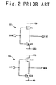
- Fig. 2 is a diagram showing the configuration of a pre-buffer output circuit.
- the conventional differential output circuit includes a pre-buffer 100 for outputting a main buffer drive signal MINT/MINB, which is a differential signal for driving a main buffer 200, from an input single phase signal IN; and the main buffer 200 which is connected to the pre-buffer 100 and outputs a differential output signal of signals OUTT/OUTB corresponding to the signal levels of the main buffer drive signal MINT/MINB.
- the pre-buffer 100 includes CMOS circuits 101 and 102 for generating the differential input signal DINT/DINB from the input single phase signal IN; and a pre-buffer output circuit 103 for outputting the main buffer drive signal MINT/MINB for driving the main buffer 200 having a large transistor size.
- the pre-buffer output circuit 103 includes a CMOS circuit 105 to which a positive phase input signal DINT of the differential input signal DINT/DINB is supplied; and a CMOS circuit 104 to which a negative phase input signal DINB is supplied.
- the CMOS circuit 104 has a P-channel MOS transistor P11 and an N-channel MOS transistor N22 between a power source voltage VDD and a ground voltage GND and outputs the positive phase drive signal MINT that is an inversion of the negative phase input signal DINB.
- the CMOS circuit 105 has a P-channel MOS transistor P110 and an N-channel MOS transistor N220 between the power source voltage VDD and the ground voltage GND and outputs the negative phase drive signal MINB that is a inversion of the positive phase input signal DINT.
- the pre-buffer 100 outputs to the main buffer 200 a main buffer drive signal MINT/MINB composed of the positive phase drive signal MINT and the negative phase drive signal MINB which are logically opposite to each other.
- the main buffer 200 includes an N-channel MOS transistor N30 to which the positive phase drive signal MINT outputted from the pre-buffer 100 is supplied; and an N-channel MOS transistor N40 to which the negative phase drive signal MINB is supplied.
- the N-channel MOS transistor N30 and the N-channel MOS transistor N40 are connected through resistors R30 and R40 to the power source voltage VDD, respectively, and connected through a current source N50 to the ground voltage GND.
- the power source voltage VDD of the main buffer 200 may be different from the power source voltage VDD of the pre-buffer 100.
- the ON/OFF states of the N-channel MOS transistor N40 and the N-channel MOS transistor N30 are controlled in accordance with the signal levels of the main buffer drive signal MINT/MINB.
- the differential output signal OUTT/OUTB composed of the positive phase output signal OUTT and the negative phase output signal OUTB which are outputted from the respective drains of the transistors N40 and 30 are outputted.
- the variation in Tpd (a delay time between pins) in the differential input signal DINT/DINB and the main buffer drive signal MINT/MINB causes a problem that the VCM of the differential output signal OUTT/OUTB from the main buffer 200 is extremely varied.
- the CMOS circuit 104 and the CMOS circuit 105 which are independent of each other, output the positive phase drive signal MINT and the negative phase drive signal MINB, respectively.
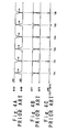
- Figs. 3A to 3C, 4A to 4C, 5A to 5C and 6A to 6C show the signal waveforms of the differential output signals OUTT/OUTB and VCM (OUTT+OUTB) when the main buffer drive signal MINT/MINB whose peak voltages are from the VDD to the GND is supplied to the main buffer 200 in the differential output circuit shown in Fig. 1.
- Figs. 4A to 4C shows the waveforms of the main buffer drive signal MINT/MINB, the differential output signal OUTT/OUTB and the VCM, when the positive phase drive signal MINT of the pre-buffer output circuit 103 is delayed rather than the negative phase drive signal MINB.
- the falling time from a high level to a low level in the positive phase drive signal MINT or the rising time from the low level to the high level is always delayed than the rising time from the low level to the high level in the negative phase drive signal MINB or the falling time from the high level to the low level.
- the cross point of the main buffer drive signal MINT/MINB is on a high voltage side (VDD side) at times T41, T43, T45 and so on, and the cross point is on a low voltage side (GND side) at times T42, T44, T46 and so on.
- VDD side high voltage side
- GND side low voltage side
- the cross points of the differential output signal OUTT/OUTB are alternately varied between the high voltage side (the times T42, T44 and so on) and the middle point (the times T41, T43 and so on) between the high level and the low level.
- the VCM is varied at the value within a ruled allowable range.
- the cross points of the differential output signal OUTT/OUTB are on the high voltage side (the times T42, T44 and so on)
- the VCM is varied in an undesirable range.
- Figs. 5A to 5C shows the time charts of the main buffer drive signal MINT/MINB, the differential output signal OUTT/OUTB and the VCM when the positive phase drive signal MINT of the pre-buffer output circuit 103 is advanced from the negative phase drive signal MINB.
- the falling time from the high level to the low level in the positive phase drive signal MINT or the rising time from the low level to the high level is always advanced from the rising time from the low level to the high level in the negative phase drive signal MINB or the falling time from the high level to the low level.
- the cross points of the main buffer drive signal MINT/MINB are on the low voltage side (the GND side) at times T51, T53 and so on and on the high voltage side (the VDD side) at times T52, T54 and so on. Therefore, the cross points of the differential output signal OUTT/OUTB are alternately varied between the high voltage side (the times T51, T53, T55 and so on) and the middle point (T52, T54, T56 and so on) between the high level and the low level.
- the cross points of the differential output signal OUTT/OUTB are located near the middle points (the times T52, T54, T56 and so on)
- the VCM is varied in the ruled allowable range.
- the cross points of the differential output signal OUTT/OUTB are on the high voltage side (the times T51, T53, T55 and so on)
- the VCM is varied in an undesirable range.
- Figs. 6A to 6C show the waveforms of the main buffer drive signal MINT/MINB, the differential output signal OUTT/OUTB and the VCM, when the duty of the positive phase drive signal MINT in the pre-buffer output circuit 103 is shifted to the negative phase drive signal MINB.
- the main buffer drive signal MINT/MINB in the main buffer drive signal MINT/MINB, the rising time from the low level to the high level is always delayed than the falling time from the high level to the low level.
- the cross points of the main buffer drive signal MINT/MINB are always on the low voltage side (GND side) at times T61, T62, T63, T64 and so on.
- the cross points of the differential output signal OUTT/OUTB are always on the high voltage side.
- the VCM is varied to the worst value, as compared with the variations in the VCM shown in Figs. 3A to 3C, 4A to 4C and 5A to 5C.
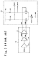
- Fig. 7 shows one example of a configuration of another conventional differential output circuit using a differential CML circuit.
- the differential output circuit includes a pre-buffer 110 for generating the main buffer drive signal MINT/MINB which is a differential signal to drive a main buffer 210, from an input single phase signal IN; and the main buffer 210 which is connected to the pre-buffer 110 and outputs the differential output signal OUTT/OUTB corresponding to the signal levels of the main buffer drive signal MINT/MINB.
- the pre-buffer 110 includes a CMOS circuit 111 and a converter 112 which generates a differential input signal DINT/DINB from the single phase signal IN; and a differential CML 113 for outputting the main buffer drive signal MINT/MINB to drive the main buffer 210 whose transistor size is large.
- the converter 112 decreases a full swing level of VDD to about 1/2 of the power supply voltage VDD for the CMOS circuit 111, and outputs the main buffer drive signal MINT/MINB.
- the pre-buffer 110 outputs the main buffer drive signal MINT/MINB, which is composed of the positive phase drive signal MINT and the negative phase drive signal MINB that are opposite in phase to each other, to the main buffer 210.
- the main buffer 210 has the same structure as the above main buffer 200 and includes an N-channel MOS transistor N41 to which the positive phase drive signal MINT outputted from the pre-buffer 110 is supplied; and an N-channel MOS transistor N31 to which the negative phase drive signal MINB is supplied.
- the N-channel MOS transistor N31 and the N-channel MOS transistor N41 are connected to the power source voltage VDD through resistors R31 and R41, respectively, and connected through a current source N51 to the ground voltage GND.
- ON and OFF of the N-channel MOS transistor N31 and the N-channel MOS transistor N41 are controlled in accordance with the signal levels of the main buffer drive signal MINT/MINB, and the differential output signal OUTT/OUTB composed of the positive phase output signal OUTT and the negative phase output signal OUTB is outputted from the respective drains of the transistors.
- the CML circuit uses a stable constant current.
- the cross points of the main buffer drive signal MINT/MINB outputted from the CML circuit can be adjusted to the vicinity of the operation point of the main buffer 210.
- the cross points of the differential output signal OUTT/OUTB are always located near the middle point between the high level and the low level. At this time, a relatively small variation is attained in the VCM.
- JP-A-Heisei, 7-273619 discloses a conventional buffer circuit that can prevent the generation of skew and reduce a timing margin.
- this conventional buffer circuit between an output of a CMOS inverter constituting an input gate stage and an input of the CMOS inverter serving as the same phase output gate stage, a push-pull circuit is provided to output a signal having the same phase as the output signal of the CMOS inverter in parallel to the CMOS inverter as a signal route, and the numbers of the gate stages to the same phase output and the negative phase output are made equal. As a result, the delay time between the same phase output and the negative phase output is removed, thereby preventing the generation of the skew.
- the cross points of the main buffer drive signal MINT/MINB are on the high voltage side
- the cross points of the differential output signal OUTT/OUTB are located near the middle point between the high level and the low level, and the VCM variation generated at this time is within the allowable range defined by the rule.
- the differential output circuit shown in Fig. 2 it is difficult to consider the variations in the power source voltage, the temperature, the process and the like, maintain the cross points of the main buffer drive signal MINT/MINB on the high voltage side, and reduce the VCM variation.
- the differential output circuit using the CLM circuit electric power consumption and circuit size in the pre-buffer 110 become greater. It causes increase in price containing a package that this circuit is installed in a macro such as a high speed serial interface macro occupying the majority of a chip and having a large electric consumption power. Therefore, the differential output circuit using this kind of CML circuit is not practicable.
- the VCM variation is 10mV (rms) although the definition is 25 mV (rms). This indicates the variation within the allowable range.
- the inventor of the present invention confirmed that the electric power consumption is about four times as compared with the conventional example using the CMOS circuit, and the macro area is about ten times.
- An object of the present invention is to provide a low amplitude differential output circuit and a serial interface circuit using the same, in which a variation of VCM is small.
- a low amplitude differential output circuit includes a pre-buffer circuit configured to output a main buffer drive signal of a first drive signal and a second drive signal which are complimentary signals, as a differential signal; and a main buffer circuit connected with the pre-buffer circuit to output a differential output signal in response to the main buffer drive signal.
- Each of the first drive signal and the second drive signal has an amplitude between a first voltage and a second voltage, and the first drive signal and the second drive signal take a same voltage between the first voltage and a middle voltage between the first voltage and the second voltage.
- the pre-buffer circuit may include a first CMOS circuit configured to output a first input signal of a positive phase in response to an external input signal; a second CMOS circuit configured to output a second input signal obtained by inverting the first input signal from the first CMOS circuit; and a pre-buffer output circuit connected with the first and second CMOS circuits and configured to output the main buffer drive signal to the main buffer circuit in response to the first input signal and the second input signal.
- the pre-buffer output circuit may include a first CMOS inverter having a first MOS transistor and a second MOS transistor between the first voltage and the second voltage; and a second CMOS inverter having a third MOS transistor and a fourth MOS transistor between the first voltage and the second voltage.
- the first CMOS inverter includes a fifth MOS transistor between the first MOS transistor and the second MOS transistor
- the second CMOS inverter comprises a sixth MOS transistor between the third MOS transistor of and the fourth MOS transistor.
- a first output terminal as a node between the first MOS transistor of and the fifth MOS transistor is connected with a gate of the sixth MOS transistor, and a second output terminal as a node between the third MOS transistor and the sixth MOS transistor is connected with a gate of the fifth MOS transistor.
- the first CMOS inverter outputs the second drive signal from the first output terminal in response to the first input signal
- the second CMOS inverter outputs the first drive signal from the second output terminal in response to the second input signal.
- the first and third MOS transistors may be P-channel MOS transistors, and the second, fourth, fifth, sixth, seventh, and eighth MOS transistors may be N-channel transistors.
- the second, fourth, fifth, sixth, seventh and eighth MOS transistors may be P-channel MOS transistors, and the first and third MOS transistors may be N-channel transistors.
- the main buffer circuit may include a differential transistor pair of seventh and eighth MOS transistor between the first voltage and the second voltage.
- the second output terminal is connected with a gate of the seventh MOS transistor, and the first output terminal is connected with a gate of the eighth MOS transistor.
- the first output signal is outputted from a drain of the seventh MOS transistor, and the second output signal is outputted from a drain of the eighth MOS transistor.
- the main buffer drive signal may be outputted such that one of the first and second drive signals is raised and then the other is fallen.
- the main buffer drive signal may be outputted such that one of the first and second drive signals is fallen and then the other is raised.
- AA serial transmission interface includes the above low amplitude differential output circuit connected with a first integrated circuit; and a transmission path connected with the low amplitude differential output circuit and a second integrated circuit.
- the low amplitude differential output circuit outputs a signal from the first integrated circuit to the second integrated circuit through the transmission path.
- a method of controlling VCM (Common Mode Voltage) in a low amplitude differential output circuit is achieved by generating a first input signal of a positive phase in response to an external input signal; by generating a second input signal obtained by inverting the first input signal; by generating a main buffer drive signal of first and second drive signals, which are complimentary, from the first and second input signal; and by generating a differential output signal in response to the main buffer drive signal.
- Each of the first drive signal and the second drive signal has an amplitude between a first voltage and a second voltage, and the first drive signal and the second drive signal take a same voltage between the first voltage and a middle voltage between the first voltage and the second voltage.
- the generating a main buffer drive signal may be achieved by generating the second drive signal from a first output terminal in response to the first input signal; and by generating the first drive signal from a second output terminal in response to the second input signal.
- the generating a main buffer drive signal may be achieved by generating the main buffer drive signal such that one of the first and second drive signals is raised and then the other is fallen.
- the generating a main buffer drive signal may be achieved by generating the main buffer drive signal such that one of the first and second drive signals is fallen and then the other is raised.
- a low amplitude differential output circuit in another aspect of the present invention, includes a pre-buffer circuit configured to output a main buffer drive signal of a first drive signal and a second drive signal which are complimentary signals, as a differential signal; and a main buffer circuit connected with the pre-buffer circuit to output a differential output signal in response to the main buffer drive signal.
- Each of the first drive signal and the second drive signal has an amplitude between a first voltage and a second voltage, and the main buffer drive signal is outputted such that one of the first and second drive signals is raised and then the other is fallen.
- the pre-buffer circuit may include a first CMOS circuit configured to output a first input signal of a positive phase in response to an external input signal; a second CMOS circuit configured to output a second input signal obtained by inverting the first input signal from the first CMOS circuit; and a pre-buffer output circuit connected with the first and second CMOS circuits and configured to output the main buffer drive signal to the main buffer circuit in response to the first input signal and the second input signal.
- the pre-buffer output circuit may include a first CMOS inverter having a first MOS transistor and a second MOS transistor between the first voltage and the second voltage; and a second CMOS inverter having a third MOS transistor and a fourth MOS transistor between the first voltage and the second voltage.
- the first CMOS inverter may include a fifth MOS transistor between the first MOS transistor and the second MOS transistor
- the second CMOS inverter may include a sixth MOS transistor between the third MOS transistor of and the fourth MOS transistor.
- a first output terminal as a node between the first MOS transistor of and the fifth MOS transistor may be connected with a gate of the sixth MOS transistor, and a second output terminal as a node between the third MOS transistor and the sixth MOS transistor may be connected with a gate of the fifth MOS transistor.
- the first CMOS inverter outputs the second drive signal from the first output terminal in response to the first input signal
- the second CMOS inverter outputs the first drive signal from the second output terminal in response to the second input signal.
- the first and third MOS transistors may be P-channel MOS transistors
- the second, fourth, fifth, sixth, seventh, and eighth MOS transistors may be N-channel transistors.
- the second, fourth, fifth, sixth, seventh and eighth MOS transistors may be P-channel MOS transistors, and the first and third MOS transistors may be N-channel transistors.
- the main buffer circuit may include a differential transistor pair of seventh and eighth MOS transistor between the first voltage and the second voltage.
- the second output terminal is connected with a gate of the seventh MOS transistor, and the first output terminal is connected with a gate of the eighth MOS transistor.
- the first output signal is outputted from a drain of the seventh MOS transistor, and the second output signal is outputted from a drain of the eighth MOS transistor.
- a low amplitude differential output circuit includes a pre-buffer circuit configured to output a main buffer drive signal of a first drive signal and a second drive signal which are complimentary signals, as a differential signal; and a main buffer circuit connected with the pre-buffer circuit to output a differential output signal in response to the main buffer drive signal.
- Each of the first drive signal and the second drive signal has an amplitude between a first voltage and a second voltage, and the main buffer drive signal is outputted such that one of the first and second drive signals is fallen and then the other is raised.
- the serial interface circuit serially transmits a signal on a transmission path between integrated circuits.
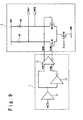
- Fig. 9 is a diagram showing a configuration of the low amplitude differential output circuit according to the first embodiment of the present invention.
- the low amplitude differential output circuit in the first embodiment includes a pre-buffer 1 and a main buffer 2.
- the pre-buffer 1 outputs a main buffer drive signal MINT/MINB as a differential signal from a single phase signal IN to drive the main buffer 2.
- the main buffer 2 is connected to the pre-buffer 1 and outputs a differential output signal OUTT/OUTB corresponding to the signal levels of the main buffer drive signal MINT/MINB.
- the pre-buffer 1 includes CMOS circuits 11 and 12 for generating the differential input signal DINT/DINB from the single phase signal IN; and a pre-buffer output circuit 13 for outputting the main buffer drive signal MINT/MINB for driving the main buffer 200 having a large transistor size.
- the pre-buffer output circuit 13 includes a CMOS circuit 14 and a CMOS circuit 15.
- the CMOS circuit 14 receives the positive phase input signal DINT of the differential input signal DINT/DINB, and the CMOS circuit 15 receives the negative phase input signal DINB thereof.
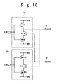
- the CMOS circuit 14 has a P-channel MOS transistor P1 and an N-channel MOS transistor N2 between the power source voltage VDD and the ground voltage GND, and outputs a negative phase drive signal MINB as an inversion signal of the input positive phase input signal DINT from an output terminal M1. Also, an N-channel MOS transistor N1 is connected between the output terminal M1 and a drain of the N-channel MOS transistor N2. A gate of the N-channel MOS transistor N1 is connected to an output terminal M2 of the CMOS circuit 15.
- the CMOS circuit 15 has a P-channel MOS transistor P10 and an N-channel MOS transistor N20 between the power source voltage VDD and the ground voltage GND, and outputs a positive phase drive signal MINT as an inversion signal of the input negative phase input signal DINT, from the output terminal M2. Also, the N-channel MOS transistor N10 is connected between the output terminal M2 and a drain of the N-channel MOS transistor N20. A gate of the N-channel MOS transistor N10 is connected to the output terminal M1 of the CMOS circuit 14. In such a configuration, the pre-buffer 1 outputs to the main buffer 2, the main buffer drive signal MINT/MINB composed of the positive phase drive signal MINT and the negative phase drive signal MINB, which are opposite in phase to each other.
- the main buffer 2 includes an N-channel MOS transistor N4 and an N-channel MOS transistor N3.
- the N-channel MOS transistor N4 receives the positive phase drive signal MINT outputted from the pre-buffer 1, and the N-channel MOS transistor N3 receives the negative phase drive signal MINB.
- the N-channel MOS transistor N3 and the N-channel MOS transistor N4 are connected through resistors R3 and R4 to the power source voltage VDD, respectively, and connected through a current source N5 to the ground voltage GND.
- the power source voltage VDD may be different from the power source voltage VDD in the pre-buffer 1.
- ON and OFF states of the N-channel MOS transistor N3 and the N-channel MOS transistor N4 are controlled in accordance with the signal levels of the main buffer drive signal MINT/MINB, and the differential output signal OUTT/OUTB composed of the positive phase output signal OUTT and the negative phase output signal OUTB are outputted from the respective drains of the transistors.
- the low amplitude differential output circuit according to the first embodiment of the present invention has the configuration where the CMOS circuits are used.
- the lower electric power consumption and the smaller chip area can be attained.
- Figs. 11A and 11B show the waveforms of the differential input signal DINT/DINB and main buffer drive signal MINT/MINB in the pre-buffer output circuit 13.
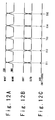
- Figs. 12A to 12C are time charts of the waveforms of the differential output signal OUTT/OUTB, which is outputted in accordance with the main buffer drive signal MINT/MINB supplied from the pre-buffer output circuit 13 to the main buffer 2, and a time chart of the VCM (OUTT+OUTB).
- the operation of the pre-buffer output circuit 13 from a time T1 to T4 will be described.
- the time T1 when the negative phase input signal DINB supplied to the pre-buffer output circuit 13 becomes a low level, the P-channel MOS transistor P10 is turned ON, and the N-channel MOS transistor N20 is turned OFF (S1).
- the voltage level of the positive phase drive signal MINT is increased by the P-channel MOS transistor P10 being turned ON (S5).
- the positive phase input signal DINT supplied to the pre-buffer output circuit 13 becomes the high level, the P-channel MOS transistor P1 is turned OFF, and the N-channel MOS transistor N2 is turned ON (S3).
- the N-channel MOS transistor N1 is in the OFF state.
- the voltage level of the negative phase drive signal MINB is not changed until the time T2 when the N-channel MOS transistor N1 is turned ON (S9).
- the voltage level of the positive phase drive signal MINT is increased to the high level, the N-channel MOS transistor N1 is turned ON (S7), and the voltage of the negative phase drive signal MINB is decreased (S9).
- the falling time of the negative phase drive signal MINB is always delayed by a period of T2-T1 from the rising time of the positive phase drive signal MINT.
- the N-channel MOS transistor N10 is turned ON (S17), and the voltage level of the positive phase drive signal MINT is decreased (S19).
- the falling time of the positive phase drive signal MINT is always delayed by a period of T4-T3 from the rising time of the negative phase drive signal MINB.
- the pre-buffer output circuit 13 outputs the main buffer drive signal MINT/MINB so as to always delay the falling timing of the signal level than the rising timing of the signal level. That is, as shown in Figs. 12A to 12C, it is always possible to supply to the main buffer 2, the main buffer drive signal MINT/MINB, signals of which always intersect each other on the higher voltage side than the middle voltage between the power source voltage VDD and the ground voltage GND.
- the main buffer drive signal MINT/MINB supplied to the main buffer 2 according to the first embodiment of the present invention has the cross points on the high voltage side, at the times T11, T12 and so on.
- the cross points of the differential output signal OUTT/OUTB are always near the middle points between the high level and the low level, and the VCM variation at the times T11, T12 and so on is suppressed.
- the low amplitude differential output circuit according to the first embodiment of the present invention can suppress the VCM variation without any influence of variation caused by the power source voltage, the temperature and the process even if using the CMOS circuits. Also, the inventor of the present invention produced a trial sample of the low amplitude differential output circuit for the high speed serial interface macro and the VCM variation of 14 mV (rms) could be attained.
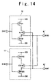
- the configuration of the low amplitude differential output circuit in the second embodiment has a main buffer 2' which uses P-channel MOS transistors P3, P4 and P5 instead of the N-channel MOS transistors N3, N4 and N5 of the main buffer 2 in the first embodiment.
- the power source voltage VDD and the ground voltage GND are replaced with each other.
- P-channel MOS transistors P2 and P20 are used instead of the N-channel MOS transistors N1 and N10 of the pre-buffer output circuit 13.
- an output terminal M1' to which the negative phase drive signal MINB is outputted is provided between the drain of the N-channel MOS transistor N2 and the drain of the P-channel MOS transistor P2, and an output terminal M2' to which the positive phase drive signal MINT is outputted is provided between the drain of the N-channel MOS transistor N20 and the drain of the P-channel MOS transistor P20.
- the gate of the P-channel MOS transistor P2 is connected to the output terminal M2', and the gate of the P-channel MOS transistor P20 is connected to the output terminal M1', respectively.
- the rising timing of the positive phase drive output signal MINT outputted from the pre-buffer output circuit 13' is delayed than the falling timing of the negative phase drive output signal MINB, and the rising timing of the negative phase drive output signal MINB is delayed than the falling timing of the positive phase drive output signal MINT.
- the cross points of the main buffer drive output signal MINT/MINB are always on the low voltage side (GND side), and the cross points of the differential output signals OUTT/OUTB are at the middle point between the high level and the low level, and the variation in the VCM value can be reduced.
- the low amplitude differential output circuit according to the present invention can reduce the influence caused by the variations in the inter-differential-signal skew and duty of the differential signal for driving the main buffer. Also, while using the CMOS circuits, it is possible to output the stable differential output signal OUTT/OUTB which is small in the VCM variation even against the variations in the power source voltage, the temperature and the process.
- the low amplitude differential output circuit In the low amplitude differential output circuit according to the present invention, it is possible to output the differential signal where the VCM variation is small and the amplitude is low.
Landscapes
- Engineering & Computer Science (AREA)
- Physics & Mathematics (AREA)
- Nonlinear Science (AREA)
- Signal Processing (AREA)
- Computer Networks & Wireless Communication (AREA)
- Computer Hardware Design (AREA)
- Computing Systems (AREA)
- General Engineering & Computer Science (AREA)
- Mathematical Physics (AREA)
- Power Engineering (AREA)
- Logic Circuits (AREA)
- Dc Digital Transmission (AREA)
- Amplifiers (AREA)
- Manipulation Of Pulses (AREA)
- Electronic Switches (AREA)
Applications Claiming Priority (1)
| Application Number | Priority Date | Filing Date | Title |
|---|---|---|---|
| JP2005056675A JP2006245828A (ja) | 2005-03-01 | 2005-03-01 | 低振幅差動出力回路及びシリアル伝送インターフェース |
Publications (2)
| Publication Number | Publication Date |
|---|---|
| EP1699135A2 true EP1699135A2 (de) | 2006-09-06 |
| EP1699135A3 EP1699135A3 (de) | 2008-07-09 |
Family
ID=36540287
Family Applications (1)
| Application Number | Title | Priority Date | Filing Date |
|---|---|---|---|
| EP06003948A Withdrawn EP1699135A3 (de) | 2005-03-01 | 2006-02-27 | Ausgang Schaltung mit kleiner Differentielle Amplitude und Schnittstelle für Serielle Übertragung |
Country Status (3)
| Country | Link |
|---|---|
| US (1) | US7741875B2 (de) |
| EP (1) | EP1699135A3 (de) |
| JP (1) | JP2006245828A (de) |
Cited By (1)
| Publication number | Priority date | Publication date | Assignee | Title |
|---|---|---|---|---|
| CN102883111A (zh) * | 2011-07-12 | 2013-01-16 | 佳能株式会社 | 固态图像感测装置 |
Families Citing this family (4)
| Publication number | Priority date | Publication date | Assignee | Title |
|---|---|---|---|---|
| JP2008160304A (ja) * | 2006-12-21 | 2008-07-10 | Nec Electronics Corp | Cml回路 |
| JP4939291B2 (ja) * | 2007-04-23 | 2012-05-23 | ルネサスエレクトロニクス株式会社 | 半導体回路 |
| JP5454582B2 (ja) * | 2009-09-09 | 2014-03-26 | 日本電気株式会社 | ラッチ回路およびラッチ回路における電位補正方法 |
| JP6217294B2 (ja) * | 2013-10-07 | 2017-10-25 | ソニー株式会社 | 光受信回路、光受信装置、および、光伝送システム |
Citations (1)
| Publication number | Priority date | Publication date | Assignee | Title |
|---|---|---|---|---|
| JPH07273619A (ja) | 1994-03-31 | 1995-10-20 | Sony Corp | バッファ回路 |
Family Cites Families (12)
| Publication number | Priority date | Publication date | Assignee | Title |
|---|---|---|---|---|
| JPS6442720A (en) * | 1987-08-10 | 1989-02-15 | Nec Corp | Clock generating circuit |
| JP2541244B2 (ja) * | 1987-10-30 | 1996-10-09 | 日本電気株式会社 | クロック発生回路 |
| JPH03222515A (ja) * | 1990-01-29 | 1991-10-01 | Mitsubishi Electric Corp | 2相クロック発生回路 |
| JPH0411410A (ja) * | 1990-04-27 | 1992-01-16 | Seiko Epson Corp | 集積回路 |
| JPH05252020A (ja) * | 1992-03-06 | 1993-09-28 | Fujitsu Ltd | Cmos駆動回路 |
| US5959492A (en) * | 1997-10-31 | 1999-09-28 | Vlsi Technology, Inc. | High speed differential driver circuitry and methods for implementing the same |
| US6172542B1 (en) * | 1998-11-16 | 2001-01-09 | Cypress Semiconductor Corp. | Selectable single ended-to differential output adjustment scheme |
| US6462589B2 (en) * | 2000-11-17 | 2002-10-08 | Tektronix, Inc. | Bus capture circuit for single-ended and differential signals |
| EP1274171A1 (de) * | 2001-07-05 | 2003-01-08 | Telefonaktiebolaget L M Ericsson (Publ) | Differentieller Leitungsempfänger |
| DE10233243B4 (de) * | 2002-07-18 | 2005-10-13 | Infineon Technologies Ag | Schaltungsanordnung zur Regeneration von Taktsignalen |
| US6803820B1 (en) * | 2003-03-26 | 2004-10-12 | Intel Corporation | Apparatus and method for reducing common-mode current in differential link |
| US7245156B2 (en) * | 2005-03-31 | 2007-07-17 | Intel Corporation | Pre-drivers for current-mode I/O drivers |
-
2005
- 2005-03-01 JP JP2005056675A patent/JP2006245828A/ja active Pending
-
2006
- 2006-02-27 EP EP06003948A patent/EP1699135A3/de not_active Withdrawn
- 2006-02-28 US US11/362,862 patent/US7741875B2/en active Active
Patent Citations (1)
| Publication number | Priority date | Publication date | Assignee | Title |
|---|---|---|---|---|
| JPH07273619A (ja) | 1994-03-31 | 1995-10-20 | Sony Corp | バッファ回路 |
Cited By (4)
| Publication number | Priority date | Publication date | Assignee | Title |
|---|---|---|---|---|
| CN102883111A (zh) * | 2011-07-12 | 2013-01-16 | 佳能株式会社 | 固态图像感测装置 |
| EP2547096A3 (de) * | 2011-07-12 | 2013-11-06 | Canon Kabushiki Kaisha | Festkörperbilderfassungsvorrichtung |
| US8810705B2 (en) | 2011-07-12 | 2014-08-19 | Canon Kabushiki Kaisha | Solid-state image sensing apparatus |
| CN102883111B (zh) * | 2011-07-12 | 2015-07-01 | 佳能株式会社 | 固态图像感测装置 |
Also Published As
| Publication number | Publication date |
|---|---|
| EP1699135A3 (de) | 2008-07-09 |
| JP2006245828A (ja) | 2006-09-14 |
| US7741875B2 (en) | 2010-06-22 |
| US20060214717A1 (en) | 2006-09-28 |
Similar Documents
| Publication | Publication Date | Title |
|---|---|---|
| KR100900965B1 (ko) | 고전압용 씨모스 전하 펌프 | |
| JP2003168969A (ja) | レベルシフト回路 | |
| EP2965425B1 (de) | Spannungspegeltrenner mit einer spannungserhöhungsschaltung mit niedriger latenz | |
| US8334709B2 (en) | Level shifter | |
| US10560084B2 (en) | Level shift circuit | |
| US7400168B2 (en) | Semiconductor device with level conversion circuit | |
| US12506481B2 (en) | Semiconductor integrated circuit, transmitter, and semiconductor device | |
| KR100686983B1 (ko) | 레벨 컨버터 회로 | |
| US20060049852A1 (en) | Sense amplifier with low common mode differential input signal | |
| US20060261851A1 (en) | Voltage conversion circuit with stable transition delay characteristic | |
| US10917095B2 (en) | Level shifting circuit and integrated circuit | |
| EP1699135A2 (de) | Ausgang Schaltung mit kleiner Differentielle Amplitude und Schnittstelle für Serielle Übertragung | |
| US9240234B2 (en) | Method of operating channel buffer block and devices including the channel buffer block | |
| US11652474B2 (en) | Semiconductor device for compensating delay fluctuation and clock transfer circuit including the same | |
| CN105763184A (zh) | 用于驱动低电压差分信号驱动电路的预驱动器 | |
| US11239842B1 (en) | Level down shifter | |
| US7564285B2 (en) | Controllable delay line and regulation compensation circuit thereof | |
| CN114640337A (zh) | 功率域改变电路以及其操作方法 | |
| US7057438B2 (en) | Output circuit and semiconductor integrated circuit incorporating it therein | |
| CN106341118A (zh) | 电平变换器电路 | |
| KR102960752B1 (ko) | 용량성 송신기 | |
| US11539366B1 (en) | Capacitive transmitter | |
| KR102674627B1 (ko) | 레벨 쉬프터 | |
| JP4273881B2 (ja) | 差動信号出力回路及びそれを内蔵した半導体集積回路 | |
| JP2025045947A (ja) | 低電圧信号レベルシフタ回路 |
Legal Events
| Date | Code | Title | Description |
|---|---|---|---|
| PUAI | Public reference made under article 153(3) epc to a published international application that has entered the european phase |
Free format text: ORIGINAL CODE: 0009012 |
|
| AK | Designated contracting states |
Kind code of ref document: A2 Designated state(s): AT BE BG CH CY CZ DE DK EE ES FI FR GB GR HU IE IS IT LI LT LU LV MC NL PL PT RO SE SI SK TR |
|
| AX | Request for extension of the european patent |
Extension state: AL BA HR MK YU |
|
| PUAL | Search report despatched |
Free format text: ORIGINAL CODE: 0009013 |
|
| AK | Designated contracting states |
Kind code of ref document: A3 Designated state(s): AT BE BG CH CY CZ DE DK EE ES FI FR GB GR HU IE IS IT LI LT LU LV MC NL PL PT RO SE SI SK TR |
|
| AX | Request for extension of the european patent |
Extension state: AL BA HR MK YU |
|
| 17P | Request for examination filed |
Effective date: 20090105 |
|
| AKX | Designation fees paid |
Designated state(s): DE GB |
|
| RAP1 | Party data changed (applicant data changed or rights of an application transferred) |
Owner name: RENESAS ELECTRONICS CORPORATION |
|
| 17Q | First examination report despatched |
Effective date: 20110510 |
|
| STAA | Information on the status of an ep patent application or granted ep patent |
Free format text: STATUS: THE APPLICATION HAS BEEN WITHDRAWN |
|
| 18W | Application withdrawn |
Effective date: 20110726 |