EP1703301A1 - Detecteur de rayonnement - Google Patents
Detecteur de rayonnement Download PDFInfo
- Publication number
- EP1703301A1 EP1703301A1 EP04724729A EP04724729A EP1703301A1 EP 1703301 A1 EP1703301 A1 EP 1703301A1 EP 04724729 A EP04724729 A EP 04724729A EP 04724729 A EP04724729 A EP 04724729A EP 1703301 A1 EP1703301 A1 EP 1703301A1
- Authority
- EP
- European Patent Office
- Prior art keywords
- photoelectron multiplier
- multiplier tube
- time
- scintillator
- light
- Prior art date
- Legal status (The legal status is an assumption and is not a legal conclusion. Google has not performed a legal analysis and makes no representation as to the accuracy of the status listed.)
- Withdrawn
Links
Images


Classifications
-
- G—PHYSICS
- G01—MEASURING; TESTING
- G01T—MEASUREMENT OF NUCLEAR OR X-RADIATION
- G01T1/00—Measuring X-radiation, gamma radiation, corpuscular radiation, or cosmic radiation
- G01T1/16—Measuring radiation intensity
- G01T1/161—Applications in the field of nuclear medicine, e.g. in vivo counting
- G01T1/164—Scintigraphy
- G01T1/1641—Static instruments for imaging the distribution of radioactivity in one or two dimensions using one or several scintillating elements; Radio-isotope cameras
- G01T1/1645—Static instruments for imaging the distribution of radioactivity in one or two dimensions using one or several scintillating elements; Radio-isotope cameras using electron optical imaging means, e.g. image intensifier tubes, coordinate photomultiplier tubes, image converter
-
- G—PHYSICS
- G01—MEASURING; TESTING
- G01T—MEASUREMENT OF NUCLEAR OR X-RADIATION
- G01T1/00—Measuring X-radiation, gamma radiation, corpuscular radiation, or cosmic radiation
- G01T1/16—Measuring radiation intensity
- G01T1/20—Measuring radiation intensity with scintillation detectors
Definitions
- the present invention relates to a detection device for radiations particularly gamma rays, more particularly, to a gamma ray detection device having a very high time resolution.
- Radiation detectors are used for the optical detection and measurement of ionizing radiations, taking advantage of a radiant relaxation phenomenon of solids.
- a short pulsed radiation is being utilizing in the fields of physics, chemistry, organism, medical treatment etc.
- PET Positron Emission Tomography
- PET Positron Emission Tomography
- the best three time resolution have been obtained up to now, the first being 124 ps measured according to a process of time-treating gamma rays with the use of a plastic scintillator and a diode amplification-type photoelectron multiplier tube ( M.Moszynski, 1993, Nuclear Instruments and Methods in Physics Research A 337 (1993) 154 ), the second being 155 ps measured according to a process of using a BaF 2 scintillator, a diode amplification-type photoelectron multiplier tube and a digital oscilloscope ( Nuclear Instruments and Methods in Physics Research A 487 (2002) 612 - 617 ), and the third being 120 ps measured according to a process of using a plastic scintillator, a diode amplification-type photoelectron multiplier tube and a digital oscilloscope ( Radiation Physics and Chemistry 68 (2003) 431 - 434 ).
- MCP built-in photoelectron multiplier tubes having characteristic high speed properties are commercially available from around the 1980.
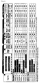
- Table 2 shows a comparison of a MCP built-in photoelectron multiplier tube with a conventional photoelectron multiplier tube.
- the MCP built-in photoelectron multiplier tube is characterized in that it is small in rise time of a wave form and also in transit time spread (T.T.S.).
- Table 2 Rise time Half bandwidth MCP built-in photoelectron multiplier (Hamamatsu photonics R3809U) 150ps 25ps Conventional high-speed photoelectron multiplier (Hamamatsu photonics H3378) 700ps 370ps
- the time resolution is determined by a statistical scatter in number of photoelectrons on the photosurface and is almost not affected by the rise time and transit time spread.
- a MCP built-in photoelectron multiplier tube and a conventional high-speed gamma ray measurement scintillator only a small number of photoelectrons can be used so that this lead to a large statistical scatter.
- poorer time resolution are obtained than those of conventional photoelectron multiplier tubes. Thus, they have not been used for the time measurement of gamma rays.
- the present invention intends to improve the time resolution for detection of gamma rays.
- the inventors have now found that much larger time resolution can be obtained than prior art values in the detection of gamma rays by using CsBr (cesium bromide) as a scintillator crystal for converting gamma rays to a light and also a MCP built-in photoelectron multiplier tube as a photoelectron multiplier tube for converting a light to an electric signal, and attained the present invention.
- CsBr cesium bromide
- the present invention is a radiation detection device comprising a CsBr crystal as a scintillator and a photoelectron multiplier tube for receiving a light from the scintillator, wherein the photoelectron multiplier tube detects a light of a wavelength of from 300 to 500 nm, and has a sensitivity permitting the detection of a single-photon, a half bandwidth of 30 ps or less relative to the single-photon and a light-receiving area of 10 mm 2 or more.
- the attenuation time of this scintillator is 50 ps or less.
- the radiation detection device of the present invention uses a CsBr crystal as a scintillator, and uses also a photoelectron multiplier tube for receiving a light from the scintillator.
- the CsBr crystal used in the present invention may be any of crystals included in such a classification.
- High purity alkali halide crystals containing CsBr are commercially provided for optical use applications from the 1960' s.
- the present invention can use such alkali halide crystals.
- the components of these compounds are Cs (cesium) and Br (bromine) in an atom ratio of 1:1. It is preferred to use those of a crystal structure of the CsCI type.
- the CsBr crystals emit a light of from 300 to 500 nm when radiated with radiations particularly gamma rays.
- a photoelectron multiplier tube is used.
- Photoelectron multiplier tubes are composed of a photosurface for converting a light to an electron, and an amplification section for amplifying the electron.
- a MCP microchannel plate
- a MCP built-in photoelectron multiplier tube is a photoelectron multiplier tube in which such an element is built whereby the detection of a single-photon is allowed and the response time bacomes rapid.
- Such a MCP built-in photoelectron multiplier tube is commercially avalable, for example, as R 3809 U series or R 5916 U series from Hamamatsu Photonics K.K. Their specifications are shown in Fig.1.
- the radiation detection device of the present invention may use, in addition to the above CsBr crystal and photoelectron multiplier tube, a combination of these components with an apparatus (es) having specifications suitably necessary for the detection of radiations.
- the CsBr crystal and MCP built-in photoelectron multiplier tube can be combined with a digital oscilloscope.
- This digital oscilloscope may be operated with an external trigger circuit.
- a known apparatus can be used according to necessity.
- the subject to be measured is preferably positron exhaustion gamma rays.
- the line sources include C - 11, N - 13, O - 15, F - 18 etc. which are used in PET, and Na - 22, G - 68 etc. which are used in the positron lifetime measurement.
- a CsBr crystal (Korth Kristalle manufactured by GMBH) was used as a scintillator. Its components are Cs and Br in an atom ratio of 1:1.
- the crystal structure is of the CsCl type. The size is 8 mm ⁇ ⁇ 8 mm. It is a polished article.
- a MCP built-in photoelectron multiplier tube (R 3809 U manufactured by Hamamatsu Photonics K.K.) was used as a photoelectron multiplier tube. Its rise time is 150 ps and transit time spread is 25 ps. Its structure is shown in Fig.2. Referring to Fig.2, CATHODE is a photosurface wherein a lihgt is converted to an electron which then comes in MCP for amplification, after which it comes out from ANODE.
- This CsBr crystal was coated over its entire surface with a silicone grease, and thereafter covered with a light protection tape with the exception of a surface to be sticked to a photoelectron multipulier tube. Then, the covered CsBr crystal was directly sticked to the light-receiving surface of the photoelectron multipulier tube to make a radiation detection device.
- 22 Na available from Japan Isotope Association; manufactured by PerkinElmer Lifescience
- the strength was 1 MBq.
- 22 Na a 1.27 MeV gamma ray and a positron were released at the same time.
- the positron changes immediately into two 0.511MeV gamma rays. At this set-up, the effect of the 1.27 MeV gamma ray can be ignored.
- the size of the light source is about 2 mm.
- Fig.3 they were connected to a digital oscilloscope (Wave Master 9600 manufactured by LeCroy; the analog band 6 GHz, the sampling frequency 20 GS/s (2 ch simultaneous)), a waveheight discriminator (Model 584 manufactured by EG & GORTEC) and a coincidence circuit (RPN - 130 manufactured by Rinei Seiki) to measure a difference of the times when two photoelectron multiplier tubes receive a light.
- the time resolution was 80 ps or less and the distance desolving power was about 12 mm.
- a line source (size:about 2 mm) was placed at a position of 20 mm apart from the CsBr crystal of one radiation detection device to measure a radiation from the light source.
- the time between the points was 5 ps, and so the width of the position of the ordinate axis (counts) at the half from the top was 16 points or less. That is, a value of 80 ps or less was obtained as the time resolution (half bandwidth) of time- difference measurement of two photoelectron extinction gamma rays (0.511 MeV, simultaneous).
- the light source was moved 10 mm towards the CsBr crystal of other radiation detection device and then the same mesuerment was conducted.
- Fig.4 The measurement results are shown in Fig.4.
- the positron source approachs 10 mm towards the right detector so that it separates 10 mm away from the left detector. It is seen from Fig.4 that, before and after this movement, the peak shifts 13.3 channels (that is, 66.6 ps).
- the light velocity is 3 cm/100 ps, and so it is anticipated that the peak position shifts 66 ps only. This anticipation was well in accordance with the above measurement results.
- the time resolution at Position A is a half bandwidth of approximately 15 ch (75 ps). This value is a sum of the attenuation time of a scintillator used, and the half bandwidth in time resolution, the difference in optical path, and other adverse effects on the time resolution of a photoelectron multiplier tube used.
- the attenuation time of a CsBr scintillator used can be determined as follows:
- the attenuation time (half-life period) of a scintillator used is termed ⁇ s
- the time resolution of a measuring instrument is termed ⁇ p
- the light path difference and other effects given to time jitters are termed ⁇ k.
- the time resolution of the entire is a square root of the sum of the square of ⁇ s, ⁇ p and ⁇ k, and therefore the following equation is obtained.
- Time Resolution 2 ⁇ s 2 + 2 ⁇ p 2 + 2 ⁇ k 2
- the light side is 75 ps from Fig.4.
- the ⁇ p is 25 ps from the catalog value.
- the ⁇ k is estimated to be 25 ps from the size of a crystal.
- the ⁇ s is 43 ps. It is seen that this substantilly corresponds to the document value (30 ps, Table 1) of CrBr.
Landscapes
- Physics & Mathematics (AREA)
- Health & Medical Sciences (AREA)
- Life Sciences & Earth Sciences (AREA)
- General Physics & Mathematics (AREA)
- High Energy & Nuclear Physics (AREA)
- Molecular Biology (AREA)
- Spectroscopy & Molecular Physics (AREA)
- Biomedical Technology (AREA)
- Engineering & Computer Science (AREA)
- General Health & Medical Sciences (AREA)
- Medical Informatics (AREA)
- Nuclear Medicine, Radiotherapy & Molecular Imaging (AREA)
- Optics & Photonics (AREA)
- Measurement Of Radiation (AREA)
- Luminescent Compositions (AREA)
- Electron Tubes For Measurement (AREA)
Applications Claiming Priority (2)
| Application Number | Priority Date | Filing Date | Title |
|---|---|---|---|
| JP2003106277 | 2003-04-10 | ||
| PCT/JP2004/004590 WO2004090571A1 (fr) | 2003-04-10 | 2004-03-31 | Detecteur de rayonnement |
Publications (1)
| Publication Number | Publication Date |
|---|---|
| EP1703301A1 true EP1703301A1 (fr) | 2006-09-20 |
Family
ID=33156907
Family Applications (1)
| Application Number | Title | Priority Date | Filing Date |
|---|---|---|---|
| EP04724729A Withdrawn EP1703301A1 (fr) | 2003-04-10 | 2004-03-31 | Detecteur de rayonnement |
Country Status (4)
| Country | Link |
|---|---|
| US (1) | US20060197028A1 (fr) |
| EP (1) | EP1703301A1 (fr) |
| JP (1) | JP4137121B2 (fr) |
| WO (1) | WO2004090571A1 (fr) |
Families Citing this family (5)
| Publication number | Priority date | Publication date | Assignee | Title |
|---|---|---|---|---|
| JP4875892B2 (ja) * | 2005-12-28 | 2012-02-15 | 大栄無線電機株式会社 | 陽電子寿命測定装置及び測定方法 |
| EP2199830B1 (fr) * | 2008-12-19 | 2014-07-02 | Leibniz-Institut für Neurobiologie | Appareil de mesure de résolution de position et procédé d'acquisition de coordonnées d'espace d'un faisceau quantique incident |
| WO2010094272A2 (fr) | 2009-02-23 | 2010-08-26 | Otto-Von-Guericke-Universität Magdeburg Medizinische Fakultät | Gamma-caméra spect, scanner spect et utilisations d'une gamma-caméra spect |
| CN108848326B (zh) * | 2018-06-13 | 2021-01-01 | 吉林大学 | 一种高动态范围mcp探测器前端读出电路及其读出方法 |
| CN110487757A (zh) * | 2019-07-29 | 2019-11-22 | 中国科学院西安光学精密机械研究所 | 倒像式像增强型超快成像探测器 |
Family Cites Families (5)
| Publication number | Priority date | Publication date | Assignee | Title |
|---|---|---|---|---|
| US2923824A (en) * | 1953-08-10 | 1960-02-02 | Philip W Martin | X-ray analysis of geological formations |
| JP2000249768A (ja) * | 1999-03-02 | 2000-09-14 | Hamamatsu Photonics Kk | シンチレータ及びそれを用いた放射線検出器 |
| US6480562B2 (en) * | 2000-12-05 | 2002-11-12 | Ge Medical Systems Global Technology Company, Llc | Apparatus and method of converting electromagnetic energy directly to electrons for computed tomography imaging |
| JP3529733B2 (ja) * | 2000-12-15 | 2004-05-24 | 独立行政法人 科学技術振興機構 | 有機無機層状ペロブスカイト型重合化合物 |
| JP3779604B2 (ja) * | 2001-01-15 | 2006-05-31 | 独立行政法人科学技術振興機構 | 放射線検出装置 |
-
2004
- 2004-03-31 WO PCT/JP2004/004590 patent/WO2004090571A1/fr not_active Ceased
- 2004-03-31 JP JP2005505214A patent/JP4137121B2/ja not_active Expired - Fee Related
- 2004-03-31 US US10/552,522 patent/US20060197028A1/en not_active Abandoned
- 2004-03-31 EP EP04724729A patent/EP1703301A1/fr not_active Withdrawn
Non-Patent Citations (1)
| Title |
|---|
| See references of WO2004090571A1 * |
Also Published As
| Publication number | Publication date |
|---|---|
| WO2004090571A1 (fr) | 2004-10-21 |
| JPWO2004090571A1 (ja) | 2006-07-06 |
| JP4137121B2 (ja) | 2008-08-20 |
| US20060197028A1 (en) | 2006-09-07 |
Similar Documents
| Publication | Publication Date | Title |
|---|---|---|
| Moses et al. | Cerium fluoride, a new fast, heavy scintillator | |
| Yoneyama et al. | Evaluation of GAGG: Ce scintillators for future space applications | |
| Melcher | Scintillation crystals for PET | |
| Aitken et al. | The fluorescent response of NaI (Tl), CsI (Tl), CsI (Na) and CaF2 (Eu) to X-rays and low energy gamma rays | |
| Kishimoto | High time resolution x‐ray measurements with an avalanche photodiode detector | |
| Ackermann et al. | Time-and energy-resolution measurements of BaF2, BC-418, LYSO and CeBr3 scintillators | |
| Moszynski | Energy resolution of scintillation detectors | |
| Hull et al. | Detection properties and internal activity of newly developed La-containing scintillator crystals | |
| Liu et al. | Light yield of an undoped CsI crystal coupled directly to a photomultiplier tube at 77 Kelvin | |
| van der Sar et al. | LaBr3: Ce and silicon photomultipliers: towards the optimal scintillating photon-counting detector | |
| Van Der Sar et al. | X-ray photon-counting using silicon photomultiplier-based scintillation detectors at high X-ray tube currents | |
| Tao et al. | Study of annihilation photon pair coincidence time resolution using prompt photon emissions in new perovskite bulk crystals | |
| RU2324204C1 (ru) | Устройство обнаружения излучения | |
| Saha | Scintillation and Semiconductor Detector | |
| EP1703301A1 (fr) | Detecteur de rayonnement | |
| Kapusta et al. | Comparison of YAP and BGO for high-resolution PET detectors | |
| JPS585387A (ja) | シンチレ−タ−物質 | |
| Moszynski et al. | Subnanosecond timing with large area avalanche photodiodes and LSO scintillator | |
| Sysoeva et al. | The non-proportional response of single crystalline oxide scintillators | |
| Takasaki et al. | Performance of a photomultiplier tube with transmissive dynodes in a high magnetic field | |
| Ranga et al. | Intrinsic resolution of compton electrons in cebr 3 scintillator using compact cct | |
| Perlman et al. | Disintegration of I 126 | |
| Wen et al. | Time resolution measurements of EJ-232Q with single-and dual-sided readouts | |
| Duxbury et al. | Preliminary results from the new large-area PETRRA positron camera | |
| Moses et al. | Gamma ray spectroscopy and timing using LSO and PIN photodiodes |
Legal Events
| Date | Code | Title | Description |
|---|---|---|---|
| PUAI | Public reference made under article 153(3) epc to a published international application that has entered the european phase |
Free format text: ORIGINAL CODE: 0009012 |
|
| 17P | Request for examination filed |
Effective date: 20051011 |
|
| AK | Designated contracting states |
Kind code of ref document: A1 Designated state(s): DE FR GB NL |
|
| RIN1 | Information on inventor provided before grant (corrected) |
Inventor name: MURAKAMI, HIDETOSHI Inventor name: SAITO, HARUO Inventor name: SHIBUYA, KENGO Inventor name: ASAI, KEISUKE |
|
| STAA | Information on the status of an ep patent application or granted ep patent |
Free format text: STATUS: THE APPLICATION HAS BEEN WITHDRAWN |
|
| 18W | Application withdrawn |
Effective date: 20080418 |