EP1705902A1 - Imaging apparatus - Google Patents
Imaging apparatus Download PDFInfo
- Publication number
- EP1705902A1 EP1705902A1 EP04807764A EP04807764A EP1705902A1 EP 1705902 A1 EP1705902 A1 EP 1705902A1 EP 04807764 A EP04807764 A EP 04807764A EP 04807764 A EP04807764 A EP 04807764A EP 1705902 A1 EP1705902 A1 EP 1705902A1
- Authority
- EP
- European Patent Office
- Prior art keywords
- read
- row
- frame
- pulse
- pixel
- Prior art date
- Legal status (The legal status is an assumption and is not a legal conclusion. Google has not performed a legal analysis and makes no representation as to the accuracy of the status listed.)
- Withdrawn
Links
Images




Classifications
-
- H—ELECTRICITY
- H04—ELECTRIC COMMUNICATION TECHNIQUE
- H04N—PICTORIAL COMMUNICATION, e.g. TELEVISION
- H04N25/00—Circuitry of solid-state image sensors [SSIS]; Control thereof
- H04N25/40—Extracting pixel data from image sensors by controlling scanning circuits, e.g. by modifying the number of pixels sampled or to be sampled
- H04N25/44—Extracting pixel data from image sensors by controlling scanning circuits, e.g. by modifying the number of pixels sampled or to be sampled by partially reading an SSIS array
- H04N25/445—Extracting pixel data from image sensors by controlling scanning circuits, e.g. by modifying the number of pixels sampled or to be sampled by partially reading an SSIS array by skipping some contiguous pixels within the read portion of the array
-
- H—ELECTRICITY
- H04—ELECTRIC COMMUNICATION TECHNIQUE
- H04N—PICTORIAL COMMUNICATION, e.g. TELEVISION
- H04N25/00—Circuitry of solid-state image sensors [SSIS]; Control thereof
- H04N25/40—Extracting pixel data from image sensors by controlling scanning circuits, e.g. by modifying the number of pixels sampled or to be sampled
- H04N25/44—Extracting pixel data from image sensors by controlling scanning circuits, e.g. by modifying the number of pixels sampled or to be sampled by partially reading an SSIS array
- H04N25/447—Extracting pixel data from image sensors by controlling scanning circuits, e.g. by modifying the number of pixels sampled or to be sampled by partially reading an SSIS array by preserving the colour pattern with or without loss of information
-
- H—ELECTRICITY
- H04—ELECTRIC COMMUNICATION TECHNIQUE
- H04N—PICTORIAL COMMUNICATION, e.g. TELEVISION
- H04N25/00—Circuitry of solid-state image sensors [SSIS]; Control thereof
- H04N25/40—Extracting pixel data from image sensors by controlling scanning circuits, e.g. by modifying the number of pixels sampled or to be sampled
- H04N25/46—Extracting pixel data from image sensors by controlling scanning circuits, e.g. by modifying the number of pixels sampled or to be sampled by combining or binning pixels
-
- H—ELECTRICITY
- H04—ELECTRIC COMMUNICATION TECHNIQUE
- H04N—PICTORIAL COMMUNICATION, e.g. TELEVISION
- H04N25/00—Circuitry of solid-state image sensors [SSIS]; Control thereof
- H04N25/70—SSIS architectures; Circuits associated therewith
- H04N25/76—Addressed sensors, e.g. MOS or CMOS sensors
- H04N25/779—Circuitry for scanning or addressing the pixel array
-
- H—ELECTRICITY
- H04—ELECTRIC COMMUNICATION TECHNIQUE
- H04N—PICTORIAL COMMUNICATION, e.g. TELEVISION
- H04N25/00—Circuitry of solid-state image sensors [SSIS]; Control thereof
- H04N25/70—SSIS architectures; Circuits associated therewith
- H04N25/76—Addressed sensors, e.g. MOS or CMOS sensors
- H04N25/7795—Circuitry for generating timing or clock signals
Definitions
- the present invention relates to an imaging apparatus that contains an imaging device for photo-electrically converting an optical image of every pixel and scanning it using an X-Y address to acquire an image signal.
- JPN. PAT. APPLN. KOKAI Publication No. 2002-314868 discloses the following imaging apparatus.
- the foregoing disclosed imaging apparatus can achieve wide range zooming at a high resolution.
- the foregoing Publication No. 2002-314868 discloses the following technique. According to the technique, thinning is changed in order to transform a magnification by scanning an imaging device.
- the thinning ratio is indicative of reading out one image from the imaging device every m x n pixels (m, n: natural number). Several cut angles of view are changed, and thereby, at least non-continuous zooming is possible.
- the foregoing publication has no disclosure relevant to a pattern change of thinning read when continuous images are imaged (shot). When photo-electrically converted information stored in the imaging device is read, read is carried out at a single thinning read pattern to simultaneously reset the contents. In this case, there is no problem in particular.
- the method of using both read and reset is employed if the thinning read pattern is changed every frame for the purpose of achieving both magnification transformation and anti-aliasing.
- the foregoing method has the following disadvantages. Specifically, read - non-read line changes in a continuous frame, or two time reads are carried out at a continuous frame in one line while only one-time read is carried out in another line. In brief, if various read patterns (see FIG. 9) are generated, storage time of photo-electrically converted information is different every line.
- An object of the present invention is to provide an imaging apparatus that can utilize at least stepwise optional magnification transformation and optional electronic shutter stroke via optional pattern thinning read of an imaging device, and can generate a read pulse and reset pulse of the imaging device with a simple configuration.
- Another object of the present invention is to provide an imaging apparatus that can generate an effective read pulse and reset pulse when an inter-frame operation is performed.
- an imaging apparatus having an imaging device photo-electrically converting an optical image of every pixel, and scanning the image using an X-Y address to acquire an image signal, comprising:
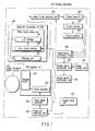
- FIG. 1 is a circuit diagram showing the configuration of an imaging apparatus according to a first embodiment of the present invention.
- An imaging apparatus 200 includes an image formation optical system 110 and an imaging unit 220.
- the imaging optical system 110 forms an optical image of a subject.
- the imaging unit 220 outputs an image signal of a predetermined area of the optical image formed by the image formation optical system 110.
- the imaging unit 220 has an aliasing MOS imaging device 222 and a read controller 224.
- the MOS imaging device 222 photo-electrically converts the optical image formed by the image formation optical system 110 to acquire a digital image signal (a set of pixel data).
- the read controller 224 is used as read means, that is, reads out the image signal acquired via the imaging device 222 in a state of thinning out pixels as the need arises.
- the read controller 224 reads out the image signal by a thinning-out operation on the imaging device 222. More specifically, an area setup unit 132 used as acquisition area setup means sets which area of the imaging device 222 should be outputted as an image signal. In this case, a read rule selecting unit 234 used as a read pattern change means selects a read rule suitable for changing a read pattern for achieving thinning read in accordance with the set area. Then, the read controller 224 reads out an image signal via pixel thinning according to the read rule thus selected. The operation of a read phase controller 230 will be described later. Incidentally, the variable power of the image signal may be set in place of setting the image signal area.
- a distortion correcting unit 140 performs predetermined distortion corrections with respect to the read image signal.
- the distortion correcting unit 140 used as distortion correction means includes a filtering unit 142 and a filter factor setup unit 144.
- the filter factor setup unit 144 has an LUT storage 146 and filter factor selector 148.
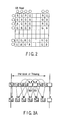
- FIG. 2 is a view to explain an example of achieving read in a state of thinning out two pixels from eight pixels in both horizontal and vertical directions. If read is carried out using the foregoing method, an image has a step, and as a result, is distorted. For this reason, the following concept is given. Specifically, as shown in the upper stage of FIG. 3A, skipped pixels (500, 501 in FIG. 3A) data are interpolated via linear interpolation using its peripheral pixels to acquire 8-pixel data. Then, the 8-pixel data is converted into 6 pixels (as shown in the lower stage of FIG. 3A).
- Thinning read is realized using the configuration of a pipeline shown in FIG. 4.
- a shift register 162 shifts a holding image signal by one in the right direction every one-time operation according to clock.
- a selector 164 selects either of the first data (C1) or the third data (C3) of neighboring five pixel data C1 to C5 held in the shift register 162 according to the state of a control signal s1.
- a selector 166 selects either of the third data (C3) or the fifth data (C5) of neighboring five pixel data C1 to C5 held in the shift register 162 according to the state of a control signal s2.
- a multiplier 174 multiplies an output d1 of the selector 164 by a weight addition coefficient k1.
- a multiplier 176 multiplies an output d2 of the selector 166 by a weight addition coefficient k2.
- An adder 178 adds the output of the multiplier 174 and the output of the multiplier 176.
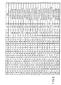
- FIG. 5 is a table to explain the pipeline processing operation (state transition) performed by a filtering unit 142 shown in FIG. 1.
- a pixel data sequence (i0, i1, i2, ...) supplied to the shift register 162 is shifted to the right direction every one-time operation according to clock.
- the coefficient k1 is read from the LUT storage 146 included in the filter factor setup unit 144 in synchrony with the clock, and thereafter, supplied to the multiplier 174.
- the coefficient k2 is read, and thereafter, supplied to the multiplier 176. Therefore, the adder 178 outputs a value of k1 ⁇ d1 + k2 ⁇ d2 as an output OUT.
- the following operations are synchronously performed, as seen from FIG. 5. Specifically, the operations are as follows. Shift of pixel data (i0, i1, i2, 7)
- pipeline processing including pixel phase operation (changeover of selector) is carried out.
- the imaging apparatus of this embodiment is based on using a dynamic image as an inputted image signal.
- Mutually lacking pixel data are interpolated between continuous two frames so that interlaced scanning interpolates lacking pixel data between two fields.
- the read phase controller 230 of FIG. 1 shifts a reference position of a pixel data range read via the read controller 224 so that images signals of continuous several frames do not lack pixel data.
- the foregoing shift is preferably in a range from 2 to 8 pixels.
- FIG. 6 and FIG. 7 are schematic views showing a state that a reference position of a read range is shifted in a 6/8 thinning read.
- [x, y] denotes a pixel position of the pixel array of the imaging device 222
- (x, y) denotes a pixel data array of a read range.
- the imaging device 222 has a pixel size of k pixels in the horizontal direction ⁇ 1 pixels in the vertical direction.
- the upper left pixel position of the imaging device 222 is expressed as [0, 0]
- the lower right pixel position is expressed as [k, 1].
- a pixel size of one frame read range is m pixels in the horizontal direction ⁇ n pixels in the vertical direction.
- the upper left read start position is expressed as (0, 0)
- the lower right read end position is expressed as (m, n).
- the frame read range of FIG. 7 is shifted by +2 pixels in the horizontal direction and by +2 pixels in the vertical direction with respect to the frame read range of FIG. 6.
- the upper left read start position (0, 0) corresponds to the upper left pixel position [0, 0] of the imaging device 222.
- ( 0 , 0 ) [ 0 , 0 ]
- the read controller 224 reads out an image signal based on a read rule that differs between several frames. Then, the filtering unit 142 carries out distortion correction filtering with respect to the image signal. Thereafter, the image signal is supplied to the image range selecting unit 240, and then, image position misalignment between frames is corrected under the control of the read phase controller 230.
- the image range selecting unit 240 selects a range common to the frame of FIG. 6 and the frame of FIG. 7. Specifically, the unit 240 selects a rectangular range using (2, 2) and (m, n) as the diagonal vertex with respect to the frame of FIG. 6.
- the unit 240 selects a rectangular range using (0, 0) to (m - 2, n - 2) as the diagonal vertex with respect to the frame of FIG. 7.
- the range selected via the image range selecting unit 240 always has (m - 2) ⁇ (n - 2) pixel data.
- the image range selecting unit 240 changes the cropping range based on the read start position information.
- Frame memories 252, 254 and 256 each comprise a FIFO (First In First Out) memory.
- the inter-frame operating unit 260 generates an image signal to be outputted using the same positioned pixel in first frame data and a second frame different from the first frame of these frame memories 252, 254 and 256.
- An image signal of a predetermined frame is stored in frame memories 252, 254 and 256 placed the image range selecting unit 240.
- the inter-frame operating unit 260 performs an inter-frame operation, and thereafter, outputs the image signal to post-stage processing systems, that is, image processing unit 152, image display unit 154 and image recording unit 156. Interpolation is made between frames, and thereby, a high quality image is obtained via a low-pass filtering effect and distortion correction effect.
- thinning read is carried out in both horizontal and vertical directions, and distortion corrections are made in both horizontal and vertical directions using pipeline processing.
- an imaging device such as a CCD performing a horizontal transfer operation from vertical transfer cannot achieve thinning read in the horizontal direction, in principle.
- all pixels are read using the foregoing expression (1), and thereby, size change must be made via one-dimensional interpolation.
- thinning read is carried out using the foregoing expression (1), and then, distortion corrections are made as above.
- the read controller 224 shifts a thinning pattern phase between continuous frames.
- reset scanning for specifying the exposure time must be made before a read.
- readout pulse and reset pulse scanning are performed.
- the scanning time is prevented from being different for every line in the frame.
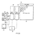
- FIG. 8 is a circuit diagram showing one configuration of a read controller 224 for performing a read operation.
- the read controller 224 includes X-shift register 301, Y-shift register 302, Y-shift register 303, timing generator (TG) 304, start pulse position registers 306, 307, selectors 308 and 309.
- the X-shift register 301 scans X-direction for reading in accordance with the X-Y address coordinate.
- the Y-shift register 302 scans lines for reading.
- the Y-shift register 303 resets lines.
- the timing generator (TG) 304 generates a signal (timing pattern) for specifying the timing of three shift registers 301 to 303.
- the start pulse position registers 306 and 307 specify a read start position.
- the selectors 308 and 309 select either of the output of the start pulse position register 306 or the output of the register 307.
- FIG. 9 shows an example of achieving thinning read, which skips two of six lines.
- FIG. 10 is a timing chart showing alternately different read patterns between frames A and B. Specifically, read and reset are repeated between frames A and B.
- Frame A Line- 1, 2, 5, 6, 7, 8, 11, 12: Read Line- 1, 2, 3, 4, 7, 8, 9, 10: Reset
- Frame B Line- 1, 2, 3, 4, 7, 8, 9, 10: Read Line- 1, 2, 5, 6, 7, 8, 11, 12: Reset
- approximately one-frame storage signal is obtained in all lines. Moreover, a timing of supplying a reset pulse is shifted (made different), and thereby, the exposure time may be varied.
- the total number of read pulses is equal to the total number of reset pulses prior to read in each frame.
- a read operation is made only for lines 5, 6, 11 and 12 of the frame A.
- frame B the read operation is reset; therefore, when a read operation is made for the next frame A, a storage signal of nearly one frame is obtained.
- lines 1, 2, 7 and 8 read and reset are made.
- the reset signal of frame A is equal to the read signal of the frame B.
- an FF circuit 310 is set up so that the contents of start pulse position registers 306 and 307 specifying a read start position is exclusively selected.
- the selecting operation of selectors 308 and 309 is controlled so that the Y-shift register 303 refers to the content of the start pulse position register 307.
- Read and reset pulses are generated at each position according to a thinning pattern generated in the TG 304 from the start position of the start pulse position registers 306 and 307.
Landscapes
- Engineering & Computer Science (AREA)
- Multimedia (AREA)
- Signal Processing (AREA)
- Transforming Light Signals Into Electric Signals (AREA)
- Studio Devices (AREA)
Abstract
Description
- The present invention relates to an imaging apparatus that contains an imaging device for photo-electrically converting an optical image of every pixel and scanning it using an X-Y address to acquire an image signal.
- There has been conventionally known an imaging apparatus, which thins out an image signal acquired by an image pickup device as the need arises to transform a magnification. For example, JPN. PAT. APPLN. KOKAI Publication No.
2002-314868 - The foregoing Publication No.
2002-314868 discloses the following technique. According to the technique, thinning is changed in order to transform a magnification by scanning an imaging device. The thinning ratio is indicative of reading out one image from the imaging device every m x n pixels (m, n: natural number). Several cut angles of view are changed, and thereby, at least non-continuous zooming is possible. However, the foregoing publication has no disclosure relevant to a pattern change of thinning read when continuous images are imaged (shot). When photo-electrically converted information stored in the imaging device is read, read is carried out at a single thinning read pattern to simultaneously reset the contents. In this case, there is no problem in particular. However, in a dynamic image, the method of using both read and reset is employed if the thinning read pattern is changed every frame for the purpose of achieving both magnification transformation and anti-aliasing. The foregoing method has the following disadvantages. Specifically, read - non-read line changes in a continuous frame, or two time reads are carried out at a continuous frame in one line while only one-time read is carried out in another line. In brief, if various read patterns (see FIG. 9) are generated, storage time of photo-electrically converted information is different every line. - The present invention has been made in view of the foregoing problem. An object of the present invention is to provide an imaging apparatus that can utilize at least stepwise optional magnification transformation and optional electronic shutter stroke via optional pattern thinning read of an imaging device, and can generate a read pulse and reset pulse of the imaging device with a simple configuration.
- Another object of the present invention is to provide an imaging apparatus that can generate an effective read pulse and reset pulse when an inter-frame operation is performed.
- To achieve the foregoing objects, according to one aspect of the present invention, there is provided an imaging apparatus having an imaging device photo-electrically converting an optical image of every pixel, and scanning the image using an X-Y address to acquire an image signal, comprising:
- read means for generating a read pulse for selecting a pixel in a row or column direction and successively performing a read operation in accordance with the image signal acquired via the imaging device, and for scanning the read pulse,
- the read means scanning a reset pulse for resetting photo-electrical conversion information recorded in each read row imaging device prior to read pulse scanning carrying out read of the selected predetermined row.
-
- FIG. 1 is a circuit diagram showing the configuration of an imaging apparatus according to a first embodiment of the present invention;
- FIG. 2 is a view to explain an example of achieving read in a state of thinning out two pixels from eight pixels in both horizontal and vertical directions;
- FIG. 3A is a conceptual view (1) to explain distortion corrections;
- FIG. 3B is a conceptual view (2) to explain distortion corrections;
- FIG. 4 is a view showing the configuration of a pipeline to realize thinning read;
- FIG. 5 is a table to explain the pipeline processing operation (state transition) by a
filtering unit 142; - FIG. 6 is a schematic view (1) showing a state that a read range reference position is shifted;
- FIG. 7 is a schematic view (2) showing a state that a read range reference position is shifted;
- FIG. 8 is a circuit diagram showing one configuration of a
read controller 224 for performing a read operation of this embodiment; - FIG. 9 is a view showing one example of read relevant to frame A and frame B; and
- FIG. 10 is a time chart to explain the detailed operation of read pulse and reset pulse in the line direction.
- An embodiment of the present invention will be explained below with reference to the accompanying drawings. FIG. 1 is a circuit diagram showing the configuration of an imaging apparatus according to a first embodiment of the present invention. An imaging apparatus 200 includes an image formation
optical system 110 and animaging unit 220. The imagingoptical system 110 forms an optical image of a subject. Theimaging unit 220 outputs an image signal of a predetermined area of the optical image formed by the image formationoptical system 110. Moreover, theimaging unit 220 has an aliasingMOS imaging device 222 and aread controller 224. TheMOS imaging device 222 photo-electrically converts the optical image formed by the image formationoptical system 110 to acquire a digital image signal (a set of pixel data). Theread controller 224 is used as read means, that is, reads out the image signal acquired via theimaging device 222 in a state of thinning out pixels as the need arises. - If there is a difference between an output image signal size and an area size on the
imaging device 222, theread controller 224 reads out the image signal by a thinning-out operation on theimaging device 222. More specifically, anarea setup unit 132 used as acquisition area setup means sets which area of theimaging device 222 should be outputted as an image signal. In this case, a readrule selecting unit 234 used as a read pattern change means selects a read rule suitable for changing a read pattern for achieving thinning read in accordance with the set area. Then, theread controller 224 reads out an image signal via pixel thinning according to the read rule thus selected. The operation of a readphase controller 230 will be described later. Incidentally, the variable power of the image signal may be set in place of setting the image signal area. - A
distortion correcting unit 140 performs predetermined distortion corrections with respect to the read image signal. Thus, thedistortion correcting unit 140 used as distortion correction means includes afiltering unit 142 and a filterfactor setup unit 144. The filterfactor setup unit 144 has anLUT storage 146 andfilter factor selector 148. - Distortion corrections of the thinning read will be explained below in detail. FIG. 2 is a view to explain an example of achieving read in a state of thinning out two pixels from eight pixels in both horizontal and vertical directions. If read is carried out using the foregoing method, an image has a step, and as a result, is distorted. For this reason, the following concept is given. Specifically, as shown in the upper stage of FIG. 3A, skipped pixels (500, 501 in FIG. 3A) data are interpolated via linear interpolation using its peripheral pixels to acquire 8-pixel data. Then, the 8-pixel data is converted into 6 pixels (as shown in the lower stage of FIG. 3A).
- In other words, the following procedure is followed, as seen from FIG. 3B. Specifically, nonuniform pixel array sampling is transformed into uniform pixel sampling. Here, consideration is given with respect to one-line read with thinning. When the upper left of FIG. 2 is used as a reference, the read pixel position becomes Ri0, Gi1 Ri2, Gi3, Ri6 and Gi7, and then, the same array rule is repeated. In the foregoing sampling, a matrix representation of distortion corrections (transformation) is as shown in
Mathematical Expression 1 given below.
- Thinning read is realized using the configuration of a pipeline shown in FIG. 4. A
shift register 162 shifts a holding image signal by one in the right direction every one-time operation according to clock. Aselector 164 selects either of the first data (C1) or the third data (C3) of neighboring five pixel data C1 to C5 held in theshift register 162 according to the state of a control signal s1. On the other hand, aselector 166 selects either of the third data (C3) or the fifth data (C5) of neighboring five pixel data C1 to C5 held in theshift register 162 according to the state of a control signal s2. Amultiplier 174 multiplies an output d1 of theselector 164 by a weight addition coefficient k1. Amultiplier 176 multiplies an output d2 of theselector 166 by a weight addition coefficient k2. Anadder 178 adds the output of themultiplier 174 and the output of themultiplier 176. - FIG. 5 is a table to explain the pipeline processing operation (state transition) performed by a
filtering unit 142 shown in FIG. 1. According to the configuration of the pipeline, a pixel data sequence (i0, i1, i2, ...) supplied to theshift register 162 is shifted to the right direction every one-time operation according to clock. In this case, C1 = i0, C2 = i1, C3 = i2 ... is used as an initial state. Thus, theselector 164 selects C1 when the control signal s1 is 1 (i.e., d1 = C1) and selects C3 when the control signal s1 is 0 (i.e., d1= C3). - On the other hand, the
selector 166 selects C3 when the control signal s2 is 1 (i.e., d2= C3) and selects C5 when the control signal s2 is 0 (i.e., d2= C5). Moreover, the coefficient k1 is read from theLUT storage 146 included in the filterfactor setup unit 144 in synchrony with the clock, and thereafter, supplied to themultiplier 174. Simultaneously, the coefficient k2 is read, and thereafter, supplied to themultiplier 176. Therefore, theadder 178 outputs a value of k1 × d1 + k2 × d2 as an output OUT. - According to this embodiment, the following operations are synchronously performed, as seen from FIG. 5. Specifically, the operations are as follows.
Shift of pixel data (i0, i1, i2, ...) - Sequential changeover of
selectors - Output of weight coefficients k1 and k2 corresponding to the thinning rule shown using the foregoing Mathematical expression (1)
- Weight
addition using multipliers adder 178 - By doing so, pipeline processing including pixel phase operation (changeover of selector) is carried out.
- The imaging apparatus of this embodiment is based on using a dynamic image as an inputted image signal. Mutually lacking pixel data are interpolated between continuous two frames so that interlaced scanning interpolates lacking pixel data between two fields. For example, the
read phase controller 230 of FIG. 1 shifts a reference position of a pixel data range read via theread controller 224 so that images signals of continuous several frames do not lack pixel data. The foregoing shift is preferably in a range from 2 to 8 pixels. - FIG. 6 and FIG. 7 are schematic views showing a state that a reference position of a read range is shifted in a 6/8 thinning read. In FIG. 6 and FIG. 7, [x, y] denotes a pixel position of the pixel array of the
imaging device 222, and (x, y) denotes a pixel data array of a read range. - As illustrated in FIG. 6 and FIG. 7, the
imaging device 222 has a pixel size of k pixels in the horizontal direction × 1 pixels in the vertical direction. Thus, the upper left pixel position of theimaging device 222 is expressed as [0, 0], and the lower right pixel position is expressed as [k, 1]. Moreover, a pixel size of one frame read range is m pixels in the horizontal direction × n pixels in the vertical direction. Thus, the upper left read start position is expressed as (0, 0), and the lower right read end position is expressed as (m, n). The frame read range of FIG. 7 is shifted by +2 pixels in the horizontal direction and by +2 pixels in the vertical direction with respect to the frame read range of FIG. 6. - In the frame of FIG. 6, the upper left read start position (0, 0) corresponds to the upper left pixel position [0, 0] of the
imaging device 222.
- The read end position (m, n) is expressed as follows.

- On the other hand, in the frame of FIG. 7, the upper left read start position is expressed as follows.

- The read end position (m, n) is expressed as follows.

- The
read controller 224 reads out an image signal based on a read rule that differs between several frames. Then, thefiltering unit 142 carries out distortion correction filtering with respect to the image signal. Thereafter, the image signal is supplied to the imagerange selecting unit 240, and then, image position misalignment between frames is corrected under the control of theread phase controller 230. In this case, the imagerange selecting unit 240 selects a range common to the frame of FIG. 6 and the frame of FIG. 7. Specifically, theunit 240 selects a rectangular range using (2, 2) and (m, n) as the diagonal vertex with respect to the frame of FIG. 6. Moreover, theunit 240 selects a rectangular range using (0, 0) to (m - 2, n - 2) as the diagonal vertex with respect to the frame of FIG. 7. The range selected via the imagerange selecting unit 240 always has (m - 2) × (n - 2) pixel data. - Previously considering a cropping area, the total number of image signals read from the
imaging device 222 has a need to consider output image size and phase shift. The imagerange selecting unit 240 changes the cropping range based on the read start position information. -
Frame memories inter-frame operating unit 260 generates an image signal to be outputted using the same positioned pixel in first frame data and a second frame different from the first frame of theseframe memories - For example, if two frames are given, a composite image out (i, j) is expressed as follows.

I (k, i, j): image signal strength of pixel position i, j of k frame
If three frames are given, a composite image out (i, j) is expressed as follows using weighted distribution.
- An image signal of a predetermined frame is stored in
frame memories range selecting unit 240. Theinter-frame operating unit 260 performs an inter-frame operation, and thereafter, outputs the image signal to post-stage processing systems, that is,image processing unit 152,image display unit 154 andimage recording unit 156. Interpolation is made between frames, and thereby, a high quality image is obtained via a low-pass filtering effect and distortion correction effect. - According to the foregoing description, thinning read is carried out in both horizontal and vertical directions, and distortion corrections are made in both horizontal and vertical directions using pipeline processing. However, an imaging device such as a CCD performing a horizontal transfer operation from vertical transfer cannot achieve thinning read in the horizontal direction, in principle. Thus, in the horizontal direction, all pixels are read using the foregoing expression (1), and thereby, size change must be made via one-dimensional interpolation. In the vertical direction, thinning read is carried out using the foregoing expression (1), and then, distortion corrections are made as above.
- As described in FIG. 6 and FIG. 7, the
read controller 224 shifts a thinning pattern phase between continuous frames. In this case, reset scanning for specifying the exposure time must be made before a read. In a frame before a read frame, readout pulse and reset pulse scanning are performed. In addition, the scanning time is prevented from being different for every line in the frame. - FIG. 8 is a circuit diagram showing one configuration of a
read controller 224 for performing a read operation. Theread controller 224 includesX-shift register 301, Y-shift register 302, Y-shift register 303, timing generator (TG) 304, start pulse position registers 306, 307,selectors X-shift register 301 scans X-direction for reading in accordance with the X-Y address coordinate. The Y-shift register 302 scans lines for reading. The Y-shift register 303 resets lines. The timing generator (TG) 304 generates a signal (timing pattern) for specifying the timing of threeshift registers 301 to 303. The start pulse position registers 306 and 307 specify a read start position. Theselectors register 307. - Line-direction read pulse and reset pulse operations will be explained below with reference to FIG. 9 and FIG. 10. FIG. 9 shows an example of achieving thinning read, which skips two of six lines. FIG. 10 is a timing chart showing alternately different read patterns between frames A and B. Specifically, read and reset are repeated between frames A and B.
Frame A: Line- 1, 2, 5, 6, 7, 8, 11, 12: Read Line- 1, 2, 3, 4, 7, 8, 9, 10: Reset Frame B: Line- 1, 2, 3, 4, 7, 8, 9, 10: Read Line- 1, 2, 5, 6, 7, 8, 11, 12: Reset - According to the timing chart shown in FIG. 10, approximately one-frame storage signal is obtained in all lines. Moreover, a timing of supplying a reset pulse is shifted (made different), and thereby, the exposure time may be varied.
- As seen from FIG. 10, the total number of read pulses is equal to the total number of reset pulses prior to read in each frame.
- According to the time chart shown in FIG. 10, a read operation is made only for
lines lines - As depicted in FIG. 6 and FIG. 7, the same read pattern is alternately shifted in phase in frames A and B. Therefore, according to the initial timing patterns stored in the
TG 304 of FIG. 8, it is sufficient for achieving one thinning. The foregoing alternate shift is realized in the following manner. In FIG. 8, anFF circuit 310 is set up so that the contents of start pulse position registers 306 and 307 specifying a read start position is exclusively selected. When the Y-shift register 302 refers to the content of the start pulse position register 306, the selecting operation ofselectors shift register 303 refers to the content of the startpulse position register 307. Read and reset pulses are generated at each position according to a thinning pattern generated in theTG 304 from the start position of the start pulse position registers 306 and 307. - According to the foregoing embodiment, it is possible to use an optional electronic shutter stroke, and to generate a read pulse and reset pulse of the imaging device with a simple configuration.
- Moreover, it is possible to generate an effective read pulse and reset pulse when an inter-frame operation is made.
- According to the present invention, it is possible to use an optional electronic shutter stroke, and to generate a read pulse and reset pulse of the imaging device with a simple configuration.
- Moreover, it is possible to generate an effective read pulse and reset pulse when an inter-frame operation is made.
Claims (10)
- An imaging apparatus having an imaging device photo-electrically converting an optical image every pixel, and scanning the image using X-Y address to acquire an image signal, comprising:read means for generating a read pulse for selecting a pixel in a row or column direction and successively performing a read operation in accordance with the image signal acquired via the imaging device, and for scanning the read pulse,the read means scanning a reset pulse for resetting photo-electrical conversion information recorded in each read row imaging device prior to read pulse scanning carrying out read of the selected predetermined row.
- The apparatus according to claim 1, wherein the image signal is acquired for every frame, and the total number of the read pulses of one frame is equal to the total number of the reset pulses prior to the read pulses.
- The apparatus according to claim 1, further comprising:frame image acquiring means for acquiring the image signal for every frame,the frame image acquiring means includes:row read timing pattern generating means for generating a row unit timing pattern, which specifies a row reading one frame of the read pulse and a skipping row to read a predetermined row of a predetermined frame, and a row read timing pattern, which has the same row unit timing pattern of one frame of the reset pulse prior to the read pulse and is different from a phase of time equivalent to an exposure time;pixel read timing pattern generating means for generating a pixel unit timing pattern to specify a row-direction read start position and a read pixel; andframe image read means for reading a pixel based on the row unit timing pattern generated by the row read timing pattern generating means and the pixel unit timing pattern generated by the pixel read timing pattern generating means.
- The apparatus according to claim 2 or 3, wherein a timing pattern of the read pulse is different between several frames.
- The apparatus according to claim 4, wherein a line unit read pulse timing pattern different between several frames and a pixel unit timing pattern are generated so that the read start position on the imaging device is different for every frame using single row unit and pixel unit timing patterns.
- The apparatus according to claim 5, wherein the read start position of the single row unit timing pattern is exclusively made different to generate the reset pulse and the read pulse.
- The apparatus according to claim 1, further comprising:variable power setup means for setting a variable power of the image signal; andread pattern change means for caning a read pattern for achieving thinning read in accordance with the variable power set by the variable power setup means.
- The apparatus according to claim 1, further comprising:acquisition area setup means for setting an acquisition area of the image signal; andread pattern change means for changing a read pattern for achieving thinning read in accordance with the acquisition area set by the acquisition area setup mean.
- The apparatus according to claim 7, further comprising:distortion correction means for correcting a distortion of the image signal read via the thinning read.
- The apparatus according to any one of claims 7 to 9, further comprising:operation means for performing an operation between several frames.
Applications Claiming Priority (2)
| Application Number | Priority Date | Filing Date | Title |
|---|---|---|---|
| JP2003434843 | 2003-12-26 | ||
| PCT/JP2004/019408 WO2005064925A1 (en) | 2003-12-26 | 2004-12-24 | Image pickup apparatus |
Publications (2)
| Publication Number | Publication Date |
|---|---|
| EP1705902A1 true EP1705902A1 (en) | 2006-09-27 |
| EP1705902A4 EP1705902A4 (en) | 2008-12-17 |
Family
ID=34736572
Family Applications (1)
| Application Number | Title | Priority Date | Filing Date |
|---|---|---|---|
| EP04807764A Withdrawn EP1705902A4 (en) | 2003-12-26 | 2004-12-24 | IMAGE INPUT APPARATUS |
Country Status (4)
| Country | Link |
|---|---|
| US (1) | US20060237630A1 (en) |
| EP (1) | EP1705902A4 (en) |
| JP (1) | JPWO2005064925A1 (en) |
| WO (1) | WO2005064925A1 (en) |
Families Citing this family (4)
| Publication number | Priority date | Publication date | Assignee | Title |
|---|---|---|---|---|
| US8040385B2 (en) | 2002-12-02 | 2011-10-18 | Olympus Corporation | Image pickup apparatus |
| DE112004002998A5 (en) * | 2004-11-10 | 2007-09-20 | Daimlerchrysler Ag | Method for a preventive protection system in a motor vehicle |
| WO2008053791A1 (en) * | 2006-10-31 | 2008-05-08 | Sanyo Electric Co., Ltd. | Imaging device and video signal generating method employed in imaging device |
| JP5101946B2 (en) * | 2007-08-03 | 2012-12-19 | キヤノン株式会社 | Imaging apparatus and imaging system |
Family Cites Families (27)
| Publication number | Priority date | Publication date | Assignee | Title |
|---|---|---|---|---|
| JPS62219754A (en) * | 1986-03-19 | 1987-09-28 | Canon Inc | image reading device |
| US4831451A (en) * | 1987-04-02 | 1989-05-16 | Texas Instruments Incorporated | Horizontal scanner for image sensor arrays |
| JP3352288B2 (en) * | 1995-07-24 | 2002-12-03 | キヤノン株式会社 | Imaging unit and imaging signal processing device |
| JP3771954B2 (en) * | 1995-08-04 | 2006-05-10 | ソニー株式会社 | Image display control apparatus and method |
| EP0809395A3 (en) * | 1996-05-22 | 1998-03-18 | Eastman Kodak Company | An X-Y addressable CMOS APS with compact pixel pitch |
| JP4229481B2 (en) * | 1996-07-31 | 2009-02-25 | オリンパス株式会社 | Imaging display system |
| JP3787927B2 (en) * | 1996-11-18 | 2006-06-21 | ソニー株式会社 | Imaging apparatus and color image signal processing method |
| JP4161384B2 (en) * | 1997-04-30 | 2008-10-08 | ソニー株式会社 | Solid-state imaging device, camera using the same, and driving method of solid-state imaging device |
| JP2000041186A (en) * | 1998-07-22 | 2000-02-08 | Minolta Co Ltd | Digital camera and control method therefor |
| JP3398081B2 (en) * | 1999-03-01 | 2003-04-21 | 三洋電機株式会社 | Digital camera |
| JP2001157106A (en) * | 1999-11-25 | 2001-06-08 | Toshiba Corp | Solid-state imaging device |
| US20020135683A1 (en) * | 1999-12-20 | 2002-09-26 | Hideo Tamama | Digital still camera system and method |
| JP4518616B2 (en) * | 2000-04-13 | 2010-08-04 | ソニー株式会社 | Solid-state imaging device, driving method thereof, and camera system |
| JP4390967B2 (en) * | 2000-04-21 | 2009-12-24 | 富士フイルム株式会社 | Electronic camera |
| JP4427701B2 (en) * | 2000-09-29 | 2010-03-10 | ソニー株式会社 | Camera device and camera function adjustment method |
| JP4192428B2 (en) * | 2001-01-09 | 2008-12-10 | ソニー株式会社 | Solid-state imaging device and image input device |
| JP3636304B2 (en) * | 2001-02-09 | 2005-04-06 | 松下電器産業株式会社 | Electronic zoom device |
| JP2002314868A (en) * | 2001-04-13 | 2002-10-25 | Olympus Optical Co Ltd | Imaging device |
| JP4503878B2 (en) * | 2001-04-27 | 2010-07-14 | オリンパス株式会社 | Imaging apparatus and imaging method |
| JP2002369083A (en) * | 2001-06-07 | 2002-12-20 | Olympus Optical Co Ltd | Imaging device |
| JP4658401B2 (en) * | 2001-07-27 | 2011-03-23 | オリンパス株式会社 | Imaging device |
| US7088392B2 (en) * | 2001-08-27 | 2006-08-08 | Ramakrishna Kakarala | Digital image system and method for implementing an adaptive demosaicing method |
| JP4717294B2 (en) * | 2001-09-20 | 2011-07-06 | キヤノン株式会社 | Image processing method, imaging apparatus, and program |
| JP4142340B2 (en) * | 2002-05-22 | 2008-09-03 | オリンパス株式会社 | Imaging device |
| US8040385B2 (en) * | 2002-12-02 | 2011-10-18 | Olympus Corporation | Image pickup apparatus |
| WO2004068852A1 (en) * | 2003-01-29 | 2004-08-12 | Olympus Corporation | Imaging system |
| US7170529B2 (en) * | 2003-10-24 | 2007-01-30 | Sigmatel, Inc. | Image processing |
-
2004
- 2004-12-24 EP EP04807764A patent/EP1705902A4/en not_active Withdrawn
- 2004-12-24 WO PCT/JP2004/019408 patent/WO2005064925A1/en not_active Ceased
- 2004-12-24 JP JP2005516660A patent/JPWO2005064925A1/en active Pending
-
2006
- 2006-06-23 US US11/474,700 patent/US20060237630A1/en not_active Abandoned
Also Published As
| Publication number | Publication date |
|---|---|
| US20060237630A1 (en) | 2006-10-26 |
| WO2005064925A1 (en) | 2005-07-14 |
| JPWO2005064925A1 (en) | 2007-12-20 |
| EP1705902A4 (en) | 2008-12-17 |
Similar Documents
| Publication | Publication Date | Title |
|---|---|---|
| US4672463A (en) | Method for emphasizing sharpness in picture scanning recording time in a picture reproducing machine | |
| US20070206207A1 (en) | Imaging apparatus | |
| EP1592236A1 (en) | Image sensing apparatus | |
| EP0337424B1 (en) | Image pickup apparatus | |
| JPH06197284A (en) | Signal processing system for correcting image aberrations and registration | |
| US20090128643A1 (en) | Image Pickup Apparatus, Method for Capturing Image, and Method for Designing Image Pickup Apparatus | |
| CN100571326C (en) | Image processing device and method for adjusting image size according to data supply speed | |
| EP0427436A2 (en) | Registration and contour correction circuit and method for solid-state camera | |
| US8040385B2 (en) | Image pickup apparatus | |
| KR100873880B1 (en) | Image processing apparatus and image processing method | |
| EP1705902A1 (en) | Imaging apparatus | |
| JP3690002B2 (en) | Image reading method, image reading apparatus, and medium on which image reading program is recorded | |
| JP3222687B2 (en) | Solid-state imaging device | |
| JP2004023384A (en) | Method for interpolating pixel signal such as tesselated green signal in interleave relation of single-plate color camera | |
| JPH042262A (en) | Picture reader | |
| US6567189B1 (en) | Image reading apparatus | |
| JP2552742B2 (en) | Adaptive contour correction circuit | |
| JP2003092764A (en) | Image signal processor | |
| JP2002290838A (en) | Video signal processing system and imaging device | |
| JPH03151784A (en) | Registration correction circuit | |
| JP4424097B2 (en) | Electronic zoom device | |
| JP2002330283A (en) | Resolution conversion method and resolution conversion device | |
| JP2002135797A (en) | Imaging device | |
| JP3632861B2 (en) | Image composition method and image composition apparatus | |
| JPH06225195A (en) | Image pickup device |
Legal Events
| Date | Code | Title | Description |
|---|---|---|---|
| PUAI | Public reference made under article 153(3) epc to a published international application that has entered the european phase |
Free format text: ORIGINAL CODE: 0009012 |
|
| 17P | Request for examination filed |
Effective date: 20060717 |
|
| AK | Designated contracting states |
Kind code of ref document: A1 Designated state(s): DE FR GB |
|
| DAX | Request for extension of the european patent (deleted) | ||
| RBV | Designated contracting states (corrected) |
Designated state(s): DE FR GB |
|
| A4 | Supplementary search report drawn up and despatched |
Effective date: 20081113 |
|
| RIC1 | Information provided on ipc code assigned before grant |
Ipc: H04N 5/335 20060101ALI20081107BHEP Ipc: H04N 9/07 20060101ALI20081107BHEP Ipc: H04N 5/232 20060101AFI20081107BHEP |
|
| STAA | Information on the status of an ep patent application or granted ep patent |
Free format text: STATUS: THE APPLICATION HAS BEEN WITHDRAWN |
|
| 18W | Application withdrawn |
Effective date: 20091007 |