EP1715522A1 - Durchsichtige LED-Anzeigevorrichtung und Verfahren zu deren Herstellung - Google Patents
Durchsichtige LED-Anzeigevorrichtung und Verfahren zu deren Herstellung Download PDFInfo
- Publication number
- EP1715522A1 EP1715522A1 EP05425255A EP05425255A EP1715522A1 EP 1715522 A1 EP1715522 A1 EP 1715522A1 EP 05425255 A EP05425255 A EP 05425255A EP 05425255 A EP05425255 A EP 05425255A EP 1715522 A1 EP1715522 A1 EP 1715522A1
- Authority
- EP
- European Patent Office
- Prior art keywords
- die
- paths
- deposited
- transparent
- stretches
- Prior art date
- Legal status (The legal status is an assumption and is not a legal conclusion. Google has not performed a legal analysis and makes no representation as to the accuracy of the status listed.)
- Granted
Links
Images


Classifications
-
- H—ELECTRICITY
- H10—SEMICONDUCTOR DEVICES; ELECTRIC SOLID-STATE DEVICES NOT OTHERWISE PROVIDED FOR
- H10H—INORGANIC LIGHT-EMITTING SEMICONDUCTOR DEVICES HAVING POTENTIAL BARRIERS
- H10H29/00—Integrated devices, or assemblies of multiple devices, comprising at least one light-emitting semiconductor element covered by group H10H20/00
- H10H29/10—Integrated devices comprising at least one light-emitting semiconductor component covered by group H10H20/00
- H10H29/14—Integrated devices comprising at least one light-emitting semiconductor component covered by group H10H20/00 comprising multiple light-emitting semiconductor components
- H10H29/142—Two-dimensional arrangements, e.g. asymmetric LED layout
-
- H—ELECTRICITY
- H10—SEMICONDUCTOR DEVICES; ELECTRIC SOLID-STATE DEVICES NOT OTHERWISE PROVIDED FOR
- H10W—GENERIC PACKAGES, INTERCONNECTIONS, CONNECTORS OR OTHER CONSTRUCTIONAL DETAILS OF DEVICES COVERED BY CLASS H10
- H10W90/00—Package configurations
- H10W90/701—Package configurations characterised by the relative positions of pads or connectors relative to package parts
- H10W90/751—Package configurations characterised by the relative positions of pads or connectors relative to package parts of bond wires
- H10W90/753—Package configurations characterised by the relative positions of pads or connectors relative to package parts of bond wires between laterally-adjacent chips
Definitions
- the present invention relates to a device for the presentation of information, characterized in that it is at the same time transparent, i.e., it enables vision of the scene at the rear of the device, and emissive, i.e., it presents the user with information in the form of light emitted by the device itself.
- a device of this type is of particular interest for the vehicle sector in so far as it enables presentation of the information on two different planes, namely, the background, i.e., the external scene visible to the user through the windows of the vehicle, such as the windscreen, rear window and side windows, and the light image generated by the device.
- the background i.e., the external scene visible to the user through the windows of the vehicle, such as the windscreen, rear window and side windows, and the light image generated by the device.
- Transparent devices based upon light-emitting diodes are already present in the known art; for example, the patent application No. EP1460609 describes a solution for transparent and programmable LED displays comprising: an array of LEDs in a row-column configuration, each row of said LEDs being connected by an electric wire, each column being connected to a transparent-conductive-oxide (TCO) layer deposited on the underlayer, said transparent layer being electrically insulated from said row of wires; and means for electrical turning-on associated to said array.
- TCO transparent-conductive-oxide
- metal wires for interconnecting the LEDs of each row enables a reduction in the voltage drops due to the electrical resistance of the row and hence use of decidedly lower supply voltages.
- Said metal wires are bonded on the underlayer of TCO only in areas corresponding to purposely provided pads obtained by cutting the layer of TCO along a closed circular path, so as to insulate said pads electrically from the corresponding column of TCO.
- the subject of the invention is a display according to Claim 1. Further advantageous characteristics are indicated in Claims 2-19 and 25-36. Also forming the subject of the invention is a method for making the display, having the characteristics indicated in Claim 20.
- the present invention is consequently able to overcome the drawbacks of the known art through:
- LED sources can be integrated directly in the form of chips or dice (multilayer semiconductor elements that emit light radiation if electrically supplied) on a printed circuit. Some typical applications are light signalling devices, headlights or other lights for motor vehicles, devices for information to the public, etc.
- the technique for fabrication of said devices goes under the name of chip-on-board (COB) technology and consists in the mounting of arrays of LED chips directly on an appropriate underlayer.
- Said technology comprises first the process known by the term "die-bonding” (i.e., thermal or electro-thermal connection of the die to the underlayer), associated to which are possible operations of "wire bonding” (electrical connection of the chip to the circuit).
- die-bonding i.e., thermal or electro-thermal connection of the die to the underlayer
- wire bonding electrical connection of the chip to the circuit.
- flip-chip methodology envisages the turning of the chip upside down and electro-thermal connection to the circuit of its pads without using wires for the electrical connection, thus excluding a further wire-bonding process.
- the connections of the pads are typically obtained by means of metal bumps (balls).
- the COB process envisages packaging or protection of the source from the external stresses using appropriate resins.
- the LED sources are arranged in a matrix configuration, in which each LED is positioned at the point of crossing-over of a row 20 and a column 10, in such a way as to be addressable individually through the application of an appropriate potential difference between said row and said column.
- the process of fabrication comprises the following steps:
- an overlayer 1' (of glass or plastic) has the function of guaranteeing planarity of the protective layer of transparent resin, not only in order to ensure transparency of the device, but also to ensure that the panel will not distort the view of the background and/or will not introduce optical power.
- the dice are of the vertical-electrode type, i.e., the anode and cathode are arranged, respectively, on the two opposite faces of the die, in such a way that the electrical contact with the rows 20 is guaranteed by the conductive resin used for the die-attach, where the electrical contact with the columns 10 of TCO is guaranteed by the connection via wire bonding between the electrode on the top face of the die and the respective pad 11.
- Figure 4 illustrates a variant of Figure 2, in which an additional insulating layer 14 is provided in the central part of the columns, in such a way as to prevent the wire from coming into contact with the columns 10 of TCO, on account of the pressure exerted on the wire used for wire bonding during the process of packaging, and from thus impairing operation of the corresponding row and column.
- the LEDs are not arranged in a matrix configuration (i.e., individually addressable), but rather are addressable in groups, with the LEDs of each group electrically connected together in parallel or in series.
- FIG 5 illustrates an example of an image that can be presented on a display according to the present invention
- each segment (31, 32, 33 and 34) represents a set of LEDs electrically connected in parallel or in series.
- Each segment which is addressable in an independent way, can be constituted by a pair of parallel paths ( Figures 6 and 7), one of which is electrically connected to the electrodes of the same type (for example, the cathodes) of a parallel of LEDs, whilst the other is electrically connected to the electrodes of the other type (for example, the anodes).
- Figure 6b presents a variant, in which an insulating layer is deposited on top of the paths 10 in areas corresponding to said points of intersection 35 so as to prevent said stretches of wire 21 from coming into electrical contact with said paths 10 on account of a deformation of the wire.
- FIG 8 A further variant of the present invention is represented in Figure 8.
- one of the two segments is constituted by a set of LEDs in series, whilst the other is constituted by a set of LEDs in parallel.
- the electrical insulation between the path 20 of the first segment and the paths 10 of the second segment is obtained in a way similar to what is indicated with reference to Figures 6 and 7.
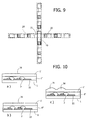
- FIG. 9 A further variant of the present invention is represented in Figure 9.
- both of the segments are constituted by a set of LEDs, connected together in series.
- the electrical insulation between the path 20 of the first segment and the path 10 of the second segment is obtained in a way similar to what is described with reference to Figures 6 and 8.
- the aim is to provide on the external surface of the underlayer 1 and/or of the overlayer 1', in areas corresponding to the dice, appropriate micro-indentations 36 along the line of connection of the dice, said micro-indentations 36 having the function of extracting light from the underlayer 1 and/or from the overlayer 1' so as to connect the points of light and generate light images in the form of continuous lines.
- Said effect can be further strengthened by the metal pads that are deposited on the paths made of TCO for the purpose of improving adhesion of the bonding operations (or else directly by the conductive paths 10, 20 that connect the sources, in the case where said paths are made of metal instead of TCO).
- said pads tend to reflect part of the light emitted by the lateral surfaces of the die; the reflected light impinges upon the micro-indentations 36, which produces an increase in the actual dimensions of the source.
- a further solution that can be adopted is to deposit the protective resin 1" in the form of paths that connect the different dice.
- the light emitted by the dice is thus in part entrapped by said paths of resin (light-guide effect) and subsequently extracted by purposely provided micro-indentations 36 made on the surface of said path of resin, or else, in the case where an overlayer 1' is used, on the surface of said overlayer.
- Said micro-indentations 36 may be in the form of cylindrical microlenses with axis perpendicular to the line of connection of the dice ( Figure 10a), generic grooves made along an axis perpendicular to the line of connection of the dice ( Figure 10b), or cylindrical lenses (one for each die) with axis perpendicular to the line of connection of the dice ( Figure 10c).
- said micro-indentations can be in the form of microlenses with rotational symmetry, each microlens having its axis of symmetry perpendicular to said underlayer 1 and passing through the centre of one of said dice.
- the micro-indentations 36 can also be simply areas with high roughness, such as to diffuse the light emitted by the LEDs.
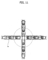
- said effect of dashed appearance of the image can be reduced or eliminated using a density of LED sources, i.e., a number of dice per unit length, such that the angular separation between two sources with respect to the eye of the user is comparable with the angular resolution of the eye.
- the angular separation between the LEDs is approximately 1 minute of arc, equal to the resolution of the eye in the fovea.
Landscapes
- Led Device Packages (AREA)
- Devices For Indicating Variable Information By Combining Individual Elements (AREA)
- Illuminated Signs And Luminous Advertising (AREA)
- Led Devices (AREA)
Priority Applications (7)
| Application Number | Priority Date | Filing Date | Title |
|---|---|---|---|
| DE602005019384T DE602005019384D1 (de) | 2005-04-21 | 2005-04-21 | Durchsichtige LED-Anzeigevorrichtung |
| AT05425255T ATE458276T1 (de) | 2005-04-21 | 2005-04-21 | Durchsichtige led-anzeigevorrichtung |
| EP05425255A EP1715522B1 (de) | 2005-04-21 | 2005-04-21 | Durchsichtige LED-Anzeigevorrichtung |
| US11/397,225 US7932524B2 (en) | 2005-04-21 | 2006-04-04 | Transparent LED display and method for manufacture thereof |
| JP2006117965A JP2006301650A (ja) | 2005-04-21 | 2006-04-21 | 透明なledディスプレイ及びその製造方法 |
| CNB2006100746421A CN100514637C (zh) | 2005-04-21 | 2006-04-21 | 透明led显示器及其制造方法 |
| JP2011001769U JP3169479U (ja) | 2005-04-21 | 2011-03-30 | 透明なledディスプレイ |
Applications Claiming Priority (1)
| Application Number | Priority Date | Filing Date | Title |
|---|---|---|---|
| EP05425255A EP1715522B1 (de) | 2005-04-21 | 2005-04-21 | Durchsichtige LED-Anzeigevorrichtung |
Publications (2)
| Publication Number | Publication Date |
|---|---|
| EP1715522A1 true EP1715522A1 (de) | 2006-10-25 |
| EP1715522B1 EP1715522B1 (de) | 2010-02-17 |
Family
ID=35058813
Family Applications (1)
| Application Number | Title | Priority Date | Filing Date |
|---|---|---|---|
| EP05425255A Expired - Lifetime EP1715522B1 (de) | 2005-04-21 | 2005-04-21 | Durchsichtige LED-Anzeigevorrichtung |
Country Status (6)
| Country | Link |
|---|---|
| US (1) | US7932524B2 (de) |
| EP (1) | EP1715522B1 (de) |
| JP (2) | JP2006301650A (de) |
| CN (1) | CN100514637C (de) |
| AT (1) | ATE458276T1 (de) |
| DE (1) | DE602005019384D1 (de) |
Cited By (3)
| Publication number | Priority date | Publication date | Assignee | Title |
|---|---|---|---|---|
| US7724212B2 (en) | 2006-02-15 | 2010-05-25 | C.R.F. Societa Consortile Per Azioni | Luminous display for automotive satellite navigation systems |
| DE102015215301A1 (de) * | 2015-08-11 | 2017-02-16 | Osram Gmbh | Leuchtdiodenanordnung und Verfahren zum Herstellen einer Leuchtdiodenanordnung |
| EP4000921A4 (de) * | 2019-07-16 | 2023-07-12 | Agc Inc. | Transparente sensorvorrichtung, laminiertes glas und verfahren zur herstellung einer transparenten sensorvorrichtung |
Families Citing this family (29)
| Publication number | Priority date | Publication date | Assignee | Title |
|---|---|---|---|---|
| US20070013057A1 (en) * | 2003-05-05 | 2007-01-18 | Joseph Mazzochette | Multicolor LED assembly with improved color mixing |
| EP1715521B1 (de) * | 2005-04-21 | 2012-02-22 | C.R.F. Società Consortile per Azioni | Anwendung einer transparenten Leuchtdiodenanzeigevorrichtung in einem Kraftfahrzeug |
| CN100585820C (zh) * | 2007-05-24 | 2010-01-27 | 宏齐科技股份有限公司 | 具高效率发光效果的发光二极管封装方法及其封装结构 |
| CN101494173B (zh) * | 2008-01-23 | 2011-04-13 | 宏齐科技股份有限公司 | 具有粗糙发光面的发光二极管芯片封装结构及其封装方法 |
| US8174103B2 (en) * | 2008-05-01 | 2012-05-08 | International Business Machines Corporation | Enhanced architectural interconnect options enabled with flipped die on a multi-chip package |
| KR101506264B1 (ko) | 2008-06-13 | 2015-03-30 | 삼성전자주식회사 | 발광 소자, 발광 장치 및 상기 발광 소자의 제조 방법 |
| US20110062482A1 (en) * | 2010-01-20 | 2011-03-17 | Bridgelux, Inc. | Apparatus And Method For Enhancing Connectability In LED Array Using Metal Traces |
| DE112011101327T5 (de) * | 2010-04-15 | 2013-01-31 | Citizen Electronics Co., Ltd. | Licht aussendende Vorrichtung |
| US10158057B2 (en) | 2010-10-28 | 2018-12-18 | Corning Incorporated | LED lighting devices |
| TWI457675B (zh) * | 2011-08-29 | 2014-10-21 | Au Optronics Corp | 畫素結構、液晶顯示面板與透明液晶顯示器 |
| US9202996B2 (en) | 2012-11-30 | 2015-12-01 | Corning Incorporated | LED lighting devices with quantum dot glass containment plates |
| KR102096874B1 (ko) * | 2012-12-14 | 2020-04-03 | 한국전자통신연구원 | 투명 디스플레이 패널을 이용한 조명 장치 및 조광 제어 방법 |
| CN103107274B (zh) * | 2013-02-19 | 2016-06-08 | 河北神通光电科技有限公司 | 一种采用过渡电极实现的led集成封装模块 |
| US9722160B2 (en) | 2014-10-31 | 2017-08-01 | Nichia Corporation | Light emitting device and adaptive driving beam headlamp system |
| JP6507729B2 (ja) | 2015-03-10 | 2019-05-08 | 日本電気硝子株式会社 | 透明導電膜付ガラス基板及びその製造方法 |
| WO2017020300A1 (zh) * | 2015-08-06 | 2017-02-09 | 林谊 | Led像素点、发光组件、发光面板和显示屏 |
| KR20170131910A (ko) | 2016-05-23 | 2017-12-01 | 주식회사 루멘스 | 발광소자 및 이를 포함하는 발광벌브 |
| JP7146748B2 (ja) | 2017-05-15 | 2022-10-04 | ソニーグループ株式会社 | 照明装置、および表示装置 |
| FR3071033B1 (fr) * | 2017-09-12 | 2021-11-19 | Valeo Vision | Procede d'obtention d'un dispositif lumineux dont l'aspect eteint est different de l'aspect allume |
| JP7200949B2 (ja) | 2018-01-25 | 2023-01-10 | Agc株式会社 | 透明表示装置、及び透明表示装置を備えた合わせガラス |
| DE102018118974A1 (de) * | 2018-08-03 | 2020-02-06 | Osram Opto Semiconductors Gmbh | Optoelektronische leuchtvorrichtung und verfahren zum steuern einer optoelektronischen leuchtvorrichtung |
| JP7351306B2 (ja) | 2018-09-04 | 2023-09-27 | Agc株式会社 | 透明表示装置、透明表示装置付きガラス板、透明表示装置付き合わせガラス、および、移動体 |
| CN111381372A (zh) * | 2018-12-28 | 2020-07-07 | 永众科技股份有限公司 | 穿透式显示设备及增强现实显示器 |
| WO2020196134A1 (ja) * | 2019-03-22 | 2020-10-01 | Agc株式会社 | 透明表示装置、透明表示装置付きガラス板、透明表示装置付き合わせガラス、及び移動体 |
| WO2021010217A1 (ja) * | 2019-07-16 | 2021-01-21 | Agc株式会社 | 透明表示装置、合わせガラス、及び透明表示装置の製造方法 |
| JP7790863B2 (ja) * | 2020-06-08 | 2025-12-23 | アルプスアルパイン株式会社 | 表示システム |
| US20260020392A1 (en) * | 2022-10-04 | 2026-01-15 | Lg Electronics Inc. | Transparent display device using light-emitting diode |
| US12315360B2 (en) * | 2023-07-13 | 2025-05-27 | Royce Hutain | Gender reveal system |
| CN117038778A (zh) * | 2023-08-18 | 2023-11-10 | 电子科技大学长三角研究院(衢州) | 一种适用于可见光通信的快速、高响应InxGa1-xN光电探测阵列 |
Citations (11)
| Publication number | Priority date | Publication date | Assignee | Title |
|---|---|---|---|---|
| EP0177134A2 (de) * | 1984-08-31 | 1986-04-09 | General Motors Corporation | Navigationsanzeigegerät mit Bildübertragung mit einem Flüssigkristall |
| JPS62215289A (ja) * | 1986-03-17 | 1987-09-21 | タキロン株式会社 | ドツトマトリクス発光表示体 |
| JPH01311501A (ja) | 1988-06-10 | 1989-12-15 | Mitsubishi Cable Ind Ltd | 発光ダイオード照明具 |
| US5278432A (en) * | 1992-08-27 | 1994-01-11 | Quantam Devices, Inc. | Apparatus for providing radiant energy |
| EP0588040A2 (de) | 1992-08-20 | 1994-03-23 | Hewlett-Packard Company | Lichtquelle und Verfahren zur Montage lichtemittierender Dioden |
| JPH08172219A (ja) * | 1994-12-20 | 1996-07-02 | Sharp Corp | 多色led素子およびその多色led素子を用いたled表示装置、並びに多色led素子の製造方法 |
| US20020084952A1 (en) * | 2000-12-29 | 2002-07-04 | Morley Roland M. | Flat panel color display with enhanced brightness and preferential viewing angles |
| WO2003012884A1 (en) | 2001-08-01 | 2003-02-13 | Nam-Young Kim | Display system |
| US20030223236A1 (en) | 2002-05-29 | 2003-12-04 | Jiahn-Chang Wu | Projection lamp with led matrix panel |
| WO2004068596A1 (en) * | 2003-01-25 | 2004-08-12 | Nam-Young Kim | Lamp module with light emitting diode |
| EP1460609A2 (de) | 2003-03-17 | 2004-09-22 | Infosight Corporation | Transparente programmierbare Leuchtdiodenanzeige und Verfahren |
Family Cites Families (23)
| Publication number | Priority date | Publication date | Assignee | Title |
|---|---|---|---|---|
| JPS5250196A (en) * | 1975-10-21 | 1977-04-21 | Seiko Instr & Electronics Ltd | Matrix dispaly device |
| US4241277A (en) * | 1979-03-01 | 1980-12-23 | Amp Incorporated | LED Display panel having bus conductors on flexible support |
| DD200295A1 (de) * | 1981-08-12 | 1983-04-06 | Guenter Claus | Led-anzeige mit hohem informationsgehalt |
| JPS58130374A (ja) * | 1982-01-29 | 1983-08-03 | 株式会社東芝 | デイスプレイ装置の製造方法 |
| JPS59143183A (ja) * | 1983-02-07 | 1984-08-16 | 日本電信電話株式会社 | 多機能平面デイスプレイ |
| JPS61237482A (ja) * | 1985-04-15 | 1986-10-22 | Toshiba Corp | 発光ダイオ−ド |
| JPH0173797U (de) * | 1987-11-05 | 1989-05-18 | ||
| JPH01273365A (ja) * | 1988-04-26 | 1989-11-01 | Furukawa Electric Co Ltd:The | 透光性表示パネル |
| GB2280534B (en) * | 1993-07-30 | 1997-04-16 | Koito Mfg Co Ltd | Display device |
| JPH0850459A (ja) * | 1994-08-08 | 1996-02-20 | Hitachi Media Electron:Kk | Led表示装置 |
| JPH0876698A (ja) * | 1994-08-31 | 1996-03-22 | Takiron Co Ltd | 発光表示体 |
| US5818404A (en) * | 1996-03-04 | 1998-10-06 | Motorola, Inc. | Integrated electro-optical package |
| US6087680A (en) * | 1997-01-31 | 2000-07-11 | Siemens Aktiengesellschaft | Led device |
| JP2001051623A (ja) * | 1999-08-05 | 2001-02-23 | Sony Corp | ディスプレイ装置 |
| US6344664B1 (en) * | 1999-12-02 | 2002-02-05 | Tera Connect Inc. | Electro-optical transceiver system with controlled lateral leakage and method of making it |
| JP2001237462A (ja) * | 2000-02-22 | 2001-08-31 | Sanyo Electric Co Ltd | Led発光装置 |
| JP2002062825A (ja) * | 2000-08-18 | 2002-02-28 | Sony Corp | 画像表示装置及びその製造方法 |
| JP2002245947A (ja) * | 2000-12-15 | 2002-08-30 | Canon Inc | 細線を有する基板及びその製造方法及び電子源基板及び画像表示装置 |
| US6864620B2 (en) * | 2000-12-22 | 2005-03-08 | Ngk Insulators, Ltd. | Matrix type actuator |
| US6650048B2 (en) * | 2001-10-19 | 2003-11-18 | Jiahn-Chang Wu | Ventilated light emitting diode matrix panel |
| KR20060079234A (ko) * | 2003-09-19 | 2006-07-05 | 소니 가부시끼 가이샤 | 백라이트 장치 및 액정 표시 장치 |
| US7123796B2 (en) * | 2003-12-08 | 2006-10-17 | University Of Cincinnati | Light emissive display based on lightwave coupling |
| US20060077669A1 (en) * | 2004-10-07 | 2006-04-13 | Robbie Thielemans | Display element and mechanical mounting interface used therein |
-
2005
- 2005-04-21 DE DE602005019384T patent/DE602005019384D1/de not_active Expired - Lifetime
- 2005-04-21 AT AT05425255T patent/ATE458276T1/de not_active IP Right Cessation
- 2005-04-21 EP EP05425255A patent/EP1715522B1/de not_active Expired - Lifetime
-
2006
- 2006-04-04 US US11/397,225 patent/US7932524B2/en not_active Expired - Fee Related
- 2006-04-21 CN CNB2006100746421A patent/CN100514637C/zh not_active Expired - Fee Related
- 2006-04-21 JP JP2006117965A patent/JP2006301650A/ja active Pending
-
2011
- 2011-03-30 JP JP2011001769U patent/JP3169479U/ja not_active Expired - Lifetime
Patent Citations (11)
| Publication number | Priority date | Publication date | Assignee | Title |
|---|---|---|---|---|
| EP0177134A2 (de) * | 1984-08-31 | 1986-04-09 | General Motors Corporation | Navigationsanzeigegerät mit Bildübertragung mit einem Flüssigkristall |
| JPS62215289A (ja) * | 1986-03-17 | 1987-09-21 | タキロン株式会社 | ドツトマトリクス発光表示体 |
| JPH01311501A (ja) | 1988-06-10 | 1989-12-15 | Mitsubishi Cable Ind Ltd | 発光ダイオード照明具 |
| EP0588040A2 (de) | 1992-08-20 | 1994-03-23 | Hewlett-Packard Company | Lichtquelle und Verfahren zur Montage lichtemittierender Dioden |
| US5278432A (en) * | 1992-08-27 | 1994-01-11 | Quantam Devices, Inc. | Apparatus for providing radiant energy |
| JPH08172219A (ja) * | 1994-12-20 | 1996-07-02 | Sharp Corp | 多色led素子およびその多色led素子を用いたled表示装置、並びに多色led素子の製造方法 |
| US20020084952A1 (en) * | 2000-12-29 | 2002-07-04 | Morley Roland M. | Flat panel color display with enhanced brightness and preferential viewing angles |
| WO2003012884A1 (en) | 2001-08-01 | 2003-02-13 | Nam-Young Kim | Display system |
| US20030223236A1 (en) | 2002-05-29 | 2003-12-04 | Jiahn-Chang Wu | Projection lamp with led matrix panel |
| WO2004068596A1 (en) * | 2003-01-25 | 2004-08-12 | Nam-Young Kim | Lamp module with light emitting diode |
| EP1460609A2 (de) | 2003-03-17 | 2004-09-22 | Infosight Corporation | Transparente programmierbare Leuchtdiodenanzeige und Verfahren |
Non-Patent Citations (2)
| Title |
|---|
| PATENT ABSTRACTS OF JAPAN vol. 014, no. 110 (M - 0943) 28 February 1990 (1990-02-28) * |
| PATENT ABSTRACTS OF JAPAN vol. 1996, no. 11 29 November 1996 (1996-11-29) * |
Cited By (3)
| Publication number | Priority date | Publication date | Assignee | Title |
|---|---|---|---|---|
| US7724212B2 (en) | 2006-02-15 | 2010-05-25 | C.R.F. Societa Consortile Per Azioni | Luminous display for automotive satellite navigation systems |
| DE102015215301A1 (de) * | 2015-08-11 | 2017-02-16 | Osram Gmbh | Leuchtdiodenanordnung und Verfahren zum Herstellen einer Leuchtdiodenanordnung |
| EP4000921A4 (de) * | 2019-07-16 | 2023-07-12 | Agc Inc. | Transparente sensorvorrichtung, laminiertes glas und verfahren zur herstellung einer transparenten sensorvorrichtung |
Also Published As
| Publication number | Publication date |
|---|---|
| JP2006301650A (ja) | 2006-11-02 |
| CN100514637C (zh) | 2009-07-15 |
| JP3169479U (ja) | 2011-08-04 |
| US20060238326A1 (en) | 2006-10-26 |
| EP1715522B1 (de) | 2010-02-17 |
| US7932524B2 (en) | 2011-04-26 |
| CN1855481A (zh) | 2006-11-01 |
| ATE458276T1 (de) | 2010-03-15 |
| DE602005019384D1 (de) | 2010-04-01 |
Similar Documents
| Publication | Publication Date | Title |
|---|---|---|
| US7932524B2 (en) | Transparent LED display and method for manufacture thereof | |
| US8283680B2 (en) | Method for manufacture of transparent devices having light emitting diodes (LED) | |
| US9666565B2 (en) | Optical device and method for manufacturing same | |
| TWM441261U (en) | Laser diode array die structure and has the laser diode array die structure of package device | |
| US12020630B1 (en) | Stacked structure, display screen, and display apparatus | |
| US10937929B2 (en) | Semiconductor unit, semiconductor device, light-emitting apparatus, display apparatus, and method of manufacturing semiconductor device | |
| US20190006326A1 (en) | Led package, led module and method for manufacturing led package | |
| CN108701434B (zh) | 视频墙模块和用于生产视频墙模块的方法 | |
| US20190259734A1 (en) | Integrated RGB LED Display Screen | |
| CN105720146A (zh) | 一种大面积电极led阵列制备方法 | |
| WO2018176656A1 (zh) | Qfn表面贴装式rgb-led封装模组及其制造方法 | |
| JP2879773B2 (ja) | 画像装置及びその製造方法 | |
| CN106847803A (zh) | 一种集成ic的表面贴装式rgb‑led封装模组 | |
| CN114096860B (zh) | 透明传感检测设备、夹层玻璃以及透明传感检测设备的制造方法 | |
| JPH10242523A (ja) | 発光ダイオード表示装置およびそれを利用した画像表示装置 | |
| CA2976591A1 (en) | Light-emitting diode apparatus and method for manufacturing a light-emitting diode apparatus | |
| US7339196B2 (en) | Packaging of SMD light emitting diodes | |
| US8183590B2 (en) | Image display apparatus having raised parts disposed on a substrate | |
| CN111162157B (zh) | 一种led显示模组 | |
| KR102333800B1 (ko) | 확장형 전극패드를 갖는 픽셀 csp 제조방법 및 그 방법에 의해 제조되는 픽셀 csp | |
| TWI878946B (zh) | 垂直型led畫素封裝體之共陰電極結構 | |
| WO2025015551A1 (zh) | 垂直型led像素封装体的共阴电极结构 | |
| JPH06230731A (ja) | Led表示装置 | |
| JP2025018208A (ja) | 垂直型led画素パッケージのコモンカソード構造 | |
| JPH1126817A (ja) | Ledモジュール |
Legal Events
| Date | Code | Title | Description |
|---|---|---|---|
| PUAI | Public reference made under article 153(3) epc to a published international application that has entered the european phase |
Free format text: ORIGINAL CODE: 0009012 |
|
| 17P | Request for examination filed |
Effective date: 20060208 |
|
| AK | Designated contracting states |
Kind code of ref document: A1 Designated state(s): AT BE BG CH CY CZ DE DK EE ES FI FR GB GR HU IE IS IT LI LT LU MC NL PL PT RO SE SI SK TR |
|
| AX | Request for extension of the european patent |
Extension state: AL BA HR LV MK YU |
|
| 17Q | First examination report despatched |
Effective date: 20070116 |
|
| AKX | Designation fees paid |
Designated state(s): AT BE BG CH CY CZ DE DK EE ES FI FR GB GR HU IE IS IT LI LT LU MC NL PL PT RO SE SI SK TR |
|
| RTI1 | Title (correction) |
Free format text: TRANSPARENT LED DISPLAY |
|
| GRAP | Despatch of communication of intention to grant a patent |
Free format text: ORIGINAL CODE: EPIDOSNIGR1 |
|
| GRAS | Grant fee paid |
Free format text: ORIGINAL CODE: EPIDOSNIGR3 |
|
| GRAA | (expected) grant |
Free format text: ORIGINAL CODE: 0009210 |
|
| AK | Designated contracting states |
Kind code of ref document: B1 Designated state(s): AT BE BG CH CY CZ DE DK EE ES FI FR GB GR HU IE IS IT LI LT LU MC NL PL PT RO SE SI SK TR |
|
| REG | Reference to a national code |
Ref country code: GB Ref legal event code: FG4D |
|
| REG | Reference to a national code |
Ref country code: CH Ref legal event code: EP |
|
| REG | Reference to a national code |
Ref country code: IE Ref legal event code: FG4D |
|
| REF | Corresponds to: |
Ref document number: 602005019384 Country of ref document: DE Date of ref document: 20100401 Kind code of ref document: P |
|
| REG | Reference to a national code |
Ref country code: NL Ref legal event code: VDEP Effective date: 20100217 |
|
| LTIE | Lt: invalidation of european patent or patent extension |
Effective date: 20100217 |
|
| PG25 | Lapsed in a contracting state [announced via postgrant information from national office to epo] |
Ref country code: ES Free format text: LAPSE BECAUSE OF FAILURE TO SUBMIT A TRANSLATION OF THE DESCRIPTION OR TO PAY THE FEE WITHIN THE PRESCRIBED TIME-LIMIT Effective date: 20100528 Ref country code: IS Free format text: LAPSE BECAUSE OF FAILURE TO SUBMIT A TRANSLATION OF THE DESCRIPTION OR TO PAY THE FEE WITHIN THE PRESCRIBED TIME-LIMIT Effective date: 20100617 Ref country code: LT Free format text: LAPSE BECAUSE OF FAILURE TO SUBMIT A TRANSLATION OF THE DESCRIPTION OR TO PAY THE FEE WITHIN THE PRESCRIBED TIME-LIMIT Effective date: 20100217 Ref country code: PT Free format text: LAPSE BECAUSE OF FAILURE TO SUBMIT A TRANSLATION OF THE DESCRIPTION OR TO PAY THE FEE WITHIN THE PRESCRIBED TIME-LIMIT Effective date: 20100617 |
|
| PG25 | Lapsed in a contracting state [announced via postgrant information from national office to epo] |
Ref country code: SI Free format text: LAPSE BECAUSE OF FAILURE TO SUBMIT A TRANSLATION OF THE DESCRIPTION OR TO PAY THE FEE WITHIN THE PRESCRIBED TIME-LIMIT Effective date: 20100217 Ref country code: PL Free format text: LAPSE BECAUSE OF FAILURE TO SUBMIT A TRANSLATION OF THE DESCRIPTION OR TO PAY THE FEE WITHIN THE PRESCRIBED TIME-LIMIT Effective date: 20100217 Ref country code: FI Free format text: LAPSE BECAUSE OF FAILURE TO SUBMIT A TRANSLATION OF THE DESCRIPTION OR TO PAY THE FEE WITHIN THE PRESCRIBED TIME-LIMIT Effective date: 20100217 Ref country code: AT Free format text: LAPSE BECAUSE OF FAILURE TO SUBMIT A TRANSLATION OF THE DESCRIPTION OR TO PAY THE FEE WITHIN THE PRESCRIBED TIME-LIMIT Effective date: 20100217 |
|
| PG25 | Lapsed in a contracting state [announced via postgrant information from national office to epo] |
Ref country code: SE Free format text: LAPSE BECAUSE OF FAILURE TO SUBMIT A TRANSLATION OF THE DESCRIPTION OR TO PAY THE FEE WITHIN THE PRESCRIBED TIME-LIMIT Effective date: 20100217 Ref country code: BE Free format text: LAPSE BECAUSE OF FAILURE TO SUBMIT A TRANSLATION OF THE DESCRIPTION OR TO PAY THE FEE WITHIN THE PRESCRIBED TIME-LIMIT Effective date: 20100217 Ref country code: CY Free format text: LAPSE BECAUSE OF FAILURE TO SUBMIT A TRANSLATION OF THE DESCRIPTION OR TO PAY THE FEE WITHIN THE PRESCRIBED TIME-LIMIT Effective date: 20100217 Ref country code: EE Free format text: LAPSE BECAUSE OF FAILURE TO SUBMIT A TRANSLATION OF THE DESCRIPTION OR TO PAY THE FEE WITHIN THE PRESCRIBED TIME-LIMIT Effective date: 20100217 Ref country code: GR Free format text: LAPSE BECAUSE OF FAILURE TO SUBMIT A TRANSLATION OF THE DESCRIPTION OR TO PAY THE FEE WITHIN THE PRESCRIBED TIME-LIMIT Effective date: 20100518 Ref country code: NL Free format text: LAPSE BECAUSE OF FAILURE TO SUBMIT A TRANSLATION OF THE DESCRIPTION OR TO PAY THE FEE WITHIN THE PRESCRIBED TIME-LIMIT Effective date: 20100217 Ref country code: RO Free format text: LAPSE BECAUSE OF FAILURE TO SUBMIT A TRANSLATION OF THE DESCRIPTION OR TO PAY THE FEE WITHIN THE PRESCRIBED TIME-LIMIT Effective date: 20100217 |
|
| PG25 | Lapsed in a contracting state [announced via postgrant information from national office to epo] |
Ref country code: SK Free format text: LAPSE BECAUSE OF FAILURE TO SUBMIT A TRANSLATION OF THE DESCRIPTION OR TO PAY THE FEE WITHIN THE PRESCRIBED TIME-LIMIT Effective date: 20100217 Ref country code: BG Free format text: LAPSE BECAUSE OF FAILURE TO SUBMIT A TRANSLATION OF THE DESCRIPTION OR TO PAY THE FEE WITHIN THE PRESCRIBED TIME-LIMIT Effective date: 20100517 Ref country code: CZ Free format text: LAPSE BECAUSE OF FAILURE TO SUBMIT A TRANSLATION OF THE DESCRIPTION OR TO PAY THE FEE WITHIN THE PRESCRIBED TIME-LIMIT Effective date: 20100217 Ref country code: MC Free format text: LAPSE BECAUSE OF NON-PAYMENT OF DUE FEES Effective date: 20100430 |
|
| REG | Reference to a national code |
Ref country code: CH Ref legal event code: PL |
|
| PLBE | No opposition filed within time limit |
Free format text: ORIGINAL CODE: 0009261 |
|
| STAA | Information on the status of an ep patent application or granted ep patent |
Free format text: STATUS: NO OPPOSITION FILED WITHIN TIME LIMIT |
|
| 26N | No opposition filed |
Effective date: 20101118 |
|
| GBPC | Gb: european patent ceased through non-payment of renewal fee |
Effective date: 20100517 |
|
| PG25 | Lapsed in a contracting state [announced via postgrant information from national office to epo] |
Ref country code: IE Free format text: LAPSE BECAUSE OF NON-PAYMENT OF DUE FEES Effective date: 20100421 Ref country code: DK Free format text: LAPSE BECAUSE OF FAILURE TO SUBMIT A TRANSLATION OF THE DESCRIPTION OR TO PAY THE FEE WITHIN THE PRESCRIBED TIME-LIMIT Effective date: 20100217 |
|
| PG25 | Lapsed in a contracting state [announced via postgrant information from national office to epo] |
Ref country code: CH Free format text: LAPSE BECAUSE OF NON-PAYMENT OF DUE FEES Effective date: 20100430 Ref country code: LI Free format text: LAPSE BECAUSE OF NON-PAYMENT OF DUE FEES Effective date: 20100430 |
|
| PG25 | Lapsed in a contracting state [announced via postgrant information from national office to epo] |
Ref country code: GB Free format text: LAPSE BECAUSE OF NON-PAYMENT OF DUE FEES Effective date: 20100517 |
|
| PG25 | Lapsed in a contracting state [announced via postgrant information from national office to epo] |
Ref country code: HU Free format text: LAPSE BECAUSE OF FAILURE TO SUBMIT A TRANSLATION OF THE DESCRIPTION OR TO PAY THE FEE WITHIN THE PRESCRIBED TIME-LIMIT Effective date: 20100818 Ref country code: LU Free format text: LAPSE BECAUSE OF NON-PAYMENT OF DUE FEES Effective date: 20100421 |
|
| PG25 | Lapsed in a contracting state [announced via postgrant information from national office to epo] |
Ref country code: TR Free format text: LAPSE BECAUSE OF FAILURE TO SUBMIT A TRANSLATION OF THE DESCRIPTION OR TO PAY THE FEE WITHIN THE PRESCRIBED TIME-LIMIT Effective date: 20100217 |
|
| REG | Reference to a national code |
Ref country code: FR Ref legal event code: PLFP Year of fee payment: 12 |
|
| REG | Reference to a national code |
Ref country code: FR Ref legal event code: PLFP Year of fee payment: 13 |
|
| REG | Reference to a national code |
Ref country code: FR Ref legal event code: PLFP Year of fee payment: 14 |
|
| PGFP | Annual fee paid to national office [announced via postgrant information from national office to epo] |
Ref country code: IT Payment date: 20190409 Year of fee payment: 15 Ref country code: DE Payment date: 20190621 Year of fee payment: 15 |
|
| PGFP | Annual fee paid to national office [announced via postgrant information from national office to epo] |
Ref country code: FR Payment date: 20190429 Year of fee payment: 15 |
|
| REG | Reference to a national code |
Ref country code: DE Ref legal event code: R119 Ref document number: 602005019384 Country of ref document: DE |
|
| PG25 | Lapsed in a contracting state [announced via postgrant information from national office to epo] |
Ref country code: DE Free format text: LAPSE BECAUSE OF NON-PAYMENT OF DUE FEES Effective date: 20201103 Ref country code: FR Free format text: LAPSE BECAUSE OF NON-PAYMENT OF DUE FEES Effective date: 20200430 |
|
| PG25 | Lapsed in a contracting state [announced via postgrant information from national office to epo] |
Ref country code: IT Free format text: LAPSE BECAUSE OF NON-PAYMENT OF DUE FEES Effective date: 20200421 |